Hubbry Logo
search button
Sign in
Homojunction
Homojunction
Comunity Hub
arrow-down
History
arrow-down
starMore
arrow-down
bob

Bob

Have a question related to this hub?

bob

Alice

Got something to say related to this hub?
Share it here.
#general is a chat channel to discuss anything related to the hub.
Hubbry Logo
search button
Sign in
Homojunction
Community hub for the Wikipedia article
logoWikipedian hub
Welcome to the community hub built on top of the Homojunction Wikipedia article. Here, you can discuss, collect, and organize anything related to Homojunction. The purpose of the hub is to connect people,...
Add your contribution
Homojunction
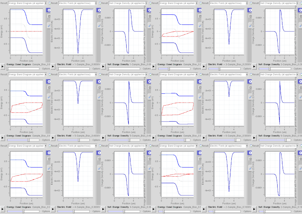
A homojunction PN junction. The band at the interface is continuous. In forward bias mode, the depletion width decreases. Both p and n junctions are doped at a 1e15/cm3 doping level, leading to built-in potential of ~0.59 V. Observe the different Quasi Fermi levels for conduction band and valence band in n and p regions (red curves).

A homojunction is a semiconductor interface that occurs between layers of similar semiconductor material;[1] these materials have equal band gaps but typically have different doping. In most practical cases a homojunction occurs at the interface between an n-type (donor doped) and p-type (acceptor doped) semiconductor such as silicon, this is called a p–n junction.

This is not a necessary condition as the only requirement is that the same semiconductor (same band gap) is found on both sides of the junction, in contrast to a heterojunction. An n-type to n-type junction, for example, would be considered a homojunction even if the doping levels are different.

The different doping level will cause band bending, and a depletion region will be formed at the interface, as shown in the figure to the right.

See also

[edit]

Notes

[edit]
  1. ^ Yang 1978, p. 141.

References

[edit]
  • Yang, Edward S (1978). Fundamentals of semiconductor devices. McGraw-Hill. ISBN 0070722366
[edit]