Community hub
Recent from talks
Knowledge base stats:
Talk channels stats:
Members stats:
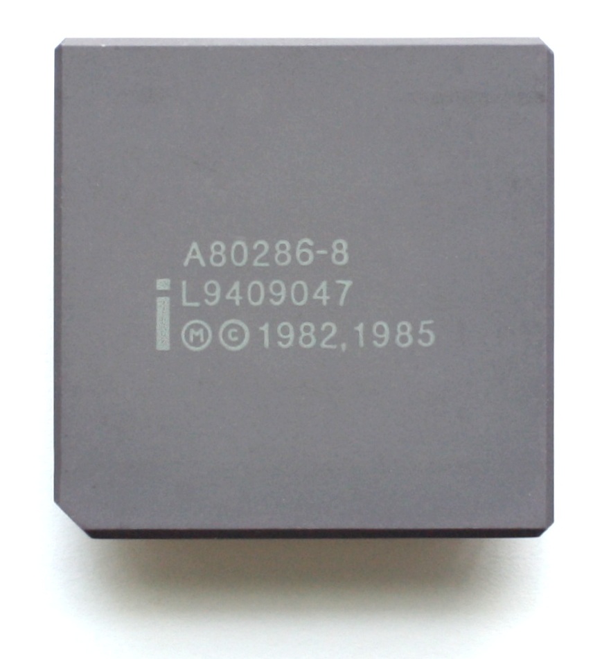
Intel 80286
The Intel 80286 (also marketed as the iAPX 286 and often called Intel 286) is a 16-bit microprocessor that was introduced on February 1, 1982. It was the first 8086-based CPU with separate, non-multiplexed address and data buses and also the first with memory management and wide protection abilities. It had a data size of 16 bits, and had an address width of 24 bits, which could address up to 16MB of memory with a suitable operating system such as Windows compared to 1MB for the 8086. The 80286 used approximately 134,000 transistors in its original nMOS (HMOS) incarnation and, just like the contemporary 80186, it can correctly execute most software written for the earlier Intel 8086 and 8088 processors.
The 80286 was employed for the IBM PC/AT, introduced in 1984, and then widely used in most PC/AT compatible computers until the early 1990s. In 1987, Intel shipped its five-millionth 80286 microprocessor.
Intel's first 80286 chips were specified for a maximum clockrate of 5, 6 or 8 MHz and later releases for 12.5 MHz. AMD and Harris later produced 16 MHz, 20 MHz and 25 MHz parts. Intel, Intersil and Fujitsu also designed fully static CMOS versions of Intel's original depletion-load nMOS implementation, largely aimed at battery-powered devices. Intel's CMOS version of the 80286 was the 80C286.
On average, the 80286 was said to have a speed of about 0.21 instructions per clock on "typical" programs, although it could be significantly faster on optimized code and in tight loops, as many instructions could execute in 2 clock cycles each. The 6 MHz, 10 MHz, and 12 MHz models were reportedly measured to operate at 0.9 MIPS, 1.5 MIPS, and 2.66 MIPS respectively.
The later E-stepping level of the 80286 was free of the several significant errata that caused problems for programmers and operating-system writers in the earlier B-step and C-step CPUs (common in the AT and AT clones). This E-2 stepping part may have been available in later 1986.
Intel second sourced this microprocessor to Fujitsu Limited in about 1985.
Intel expected the 286 to be used primarily in industrial automation, transaction processing, and telecommunications, instead of in personal computers.
The CPU was designed for multi-user systems with multitasking applications, including communications (such as automated PBXs) and real-time process control. It had 134,000 transistors and consisted of four independent units: the address unit, bus unit, instruction unit, and execution unit, organized into a loosely coupled (buffered) pipeline, just as in the 8086. It was produced in a 68-pin package, including PLCC (plastic leaded chip carrier), LCC (leadless chip carrier) and PGA (pin grid array) packages.
Hub AI
Intel 80286 AI simulator
(@Intel 80286_simulator)
Intel 80286
The Intel 80286 (also marketed as the iAPX 286 and often called Intel 286) is a 16-bit microprocessor that was introduced on February 1, 1982. It was the first 8086-based CPU with separate, non-multiplexed address and data buses and also the first with memory management and wide protection abilities. It had a data size of 16 bits, and had an address width of 24 bits, which could address up to 16MB of memory with a suitable operating system such as Windows compared to 1MB for the 8086. The 80286 used approximately 134,000 transistors in its original nMOS (HMOS) incarnation and, just like the contemporary 80186, it can correctly execute most software written for the earlier Intel 8086 and 8088 processors.
The 80286 was employed for the IBM PC/AT, introduced in 1984, and then widely used in most PC/AT compatible computers until the early 1990s. In 1987, Intel shipped its five-millionth 80286 microprocessor.
Intel's first 80286 chips were specified for a maximum clockrate of 5, 6 or 8 MHz and later releases for 12.5 MHz. AMD and Harris later produced 16 MHz, 20 MHz and 25 MHz parts. Intel, Intersil and Fujitsu also designed fully static CMOS versions of Intel's original depletion-load nMOS implementation, largely aimed at battery-powered devices. Intel's CMOS version of the 80286 was the 80C286.
On average, the 80286 was said to have a speed of about 0.21 instructions per clock on "typical" programs, although it could be significantly faster on optimized code and in tight loops, as many instructions could execute in 2 clock cycles each. The 6 MHz, 10 MHz, and 12 MHz models were reportedly measured to operate at 0.9 MIPS, 1.5 MIPS, and 2.66 MIPS respectively.
The later E-stepping level of the 80286 was free of the several significant errata that caused problems for programmers and operating-system writers in the earlier B-step and C-step CPUs (common in the AT and AT clones). This E-2 stepping part may have been available in later 1986.
Intel second sourced this microprocessor to Fujitsu Limited in about 1985.
Intel expected the 286 to be used primarily in industrial automation, transaction processing, and telecommunications, instead of in personal computers.
The CPU was designed for multi-user systems with multitasking applications, including communications (such as automated PBXs) and real-time process control. It had 134,000 transistors and consisted of four independent units: the address unit, bus unit, instruction unit, and execution unit, organized into a loosely coupled (buffered) pipeline, just as in the 8086. It was produced in a 68-pin package, including PLCC (plastic leaded chip carrier), LCC (leadless chip carrier) and PGA (pin grid array) packages.