

Community hub
0 subscribers8 pages, 0 posts
Recent from talks
All channels
Be the first to start a discussion here.
Be the first to start a discussion here.
Be the first to start a discussion here.
Be the first to start a discussion here.
Contribute something
Welcome to the community hub built to collect knowledge and have discussions related to 6264.
Nothing was collected or created yet.
from Wikipedia

The 6264 is a JEDEC-standard static RAM integrated circuit. It has a capacity of 64 Kbit (8 KB). It is produced by a wide variety of different vendors, including Hitachi, Hynix, and Cypress Semiconductor. It is available in a variety of different configurations, such as DIP, SPDIP, and SOIC. Some versions of the 6264 can run in ultra-low-power mode and retain memory when not in use, thus making them suitable for battery backup applications.
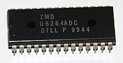
ZMD U6264 SRAM

External links
[edit]This computer-storage-related article is a stub. You can help Wikipedia by adding missing information. |
from Grokipedia
The 6264 is a JEDEC-standard static random-access memory (SRAM) integrated circuit with a capacity of 64 kilobits (8 kilobytes), organized as 8,192 words by 8 bits, designed for high-speed data storage in electronic systems.[1] It operates on a single 5 V supply and features low-power consumption, including a typical standby current of 10 µW and operational power of around 15 mW at 1 MHz, making it suitable for battery-powered or portable devices.[2] First introduced in the 1980s by manufacturers such as Hitachi, Motorola, and Samsung, the 6264 has been produced in various access time variants ranging from 70 ns to 200 ns to accommodate different performance needs in applications like embedded systems, game consoles, and early personal computers.[2] Its static design eliminates the need for external refresh circuitry or timing signals, simplifying integration compared to dynamic RAM alternatives.[3]
This configuration supports easy memory expansion in systems by daisy-chaining multiple 6264 chips via shared address and control buses, with chip select signals used for selection.[5][11]
Overview
Description
The 6264 is a JEDEC-standard static random access memory (SRAM) integrated circuit featuring an asynchronous interface, designed for high-speed data access in various electronic systems.[4] As a volatile memory device, it stores data temporarily during operation but requires continuous power to retain information, offering rapid read and write capabilities without the need for periodic refresh cycles that characterize dynamic RAM (DRAM).[4] This design makes the 6264 simpler to integrate but more power-intensive compared to DRAM alternatives.[4] Typically housed in a 28-pin dual in-line package (DIP) with a 0.6-inch width and standard 0.1-inch lead spacing, the chip supports easy mounting on circuit boards via through-hole technology.[4] Its core purpose is to provide fast, reliable random access storage for temporary data in microcomputers, peripherals, and embedded applications, with a total capacity of 64 Kbit organized as 8K words by 8 bits.[4]Capacity and Organization
The 6264 is a static random-access memory (SRAM) integrated circuit with a total capacity of 64 kilobits (Kbit), equivalent to 8 kilobytes (KB) or 65,536 bits. This capacity allows for the storage of up to 8,192 distinct 8-bit words, providing a byte-wide data interface suitable for many early microcomputer designs.[5][6] Internally, the 6264 is organized as 8,192 words by 8 bits (8K × 8), enabling efficient access to data in byte increments without the need for internal multiplexing common in dynamic RAMs. The organization is fixed as 8K × 8. Data storage relies on a static architecture using bistable latching circuits, which retain information without periodic refreshing as long as power is supplied.[5][7] Addressing in the 6264 is handled via 13 address input lines (A0 through A12), which directly select one of the 8,192 possible word locations in the memory array. These lines provide a straightforward binary decoding scheme, where the full 13-bit address is applied simultaneously to access the desired 8-bit word, supporting asynchronous operation without clock synchronization. This direct addressing simplifies integration compared to multiplexed schemes, allowing rapid random access within the chip's specified timing parameters.[5][6] Read and write operations on the 6264 are controlled asynchronously through dedicated signals, including chip enable (CE, often implemented as dual CE1 and CE2 for flexibility in power management) and write enable (WE). For a read cycle, the chip is selected by asserting the appropriate CE signals while holding WE high, placing the selected 8-bit word on the bidirectional data pins (DQ0–DQ7). In write mode, WE is asserted low with valid data and address present, latching the new byte into the addressed location. An additional output enable (OE) signal further refines read access by controlling the data bus state, ensuring high-impedance outputs when deselected to support memory expansion. This signal configuration enables reliable data transfer in bus-oriented systems.[5][7]Technical Specifications
Electrical Characteristics
The 6264 SRAM operates on a single supply voltage of 5 V ±10% (VCC = 4.5 V to 5.5 V), with ground (VSS) referenced at 0 V. This standard TTL-compatible power requirement ensures compatibility with contemporary digital logic families of the era. Data retention is possible at voltages as low as 2.0 V in CMOS variants, facilitating low-power applications.[8][5] Access times for the 6264 vary by speed grade, denoted by suffixes such as -70, -85, -100, -120, -150, and up to -200, indicating maximum read or write cycle times from 70 ns to 200 ns. For instance, the -70 variant achieves address access times (tAA) of 70 ns maximum under typical conditions (VCC = 5.0 V, TA = 25°C), while slower grades like the CDM6264CD3 extend to 200 ns for cost-sensitive or low-frequency designs. These timings support cycle times equal to access times in static operation, without the refresh requirements of DRAM.[8][9][10] Power consumption depends on the operating mode and variant. Active current (ICC) reaches up to 260 mA maximum in industrial-grade devices during full operation (outputs enabled, cycling at rated speed), though typical values are lower at 30 mA for commercial CMOS versions at 1 MHz. Standby current drops significantly, to as low as 20 mA in TTL standby mode or 15 mA in CMOS power-down (with chip enable high and inputs at extremes) for commercial variants, enabling energy-efficient deselection in multi-chip systems. Note that some manufacturers like Hitachi specify lower CMOS standby currents around 10 µA under specific conditions.[8][5] The device supports commercial (0°C to 70°C) and industrial (-40°C to 85°C) operating temperature ranges, with specifications guaranteed across these extremes for reliable performance in varied environments. Automotive-grade variants extend similar tolerances.[8][5] Input and output levels are TTL-compatible, with high-level input threshold (VIH) at 2.2 V minimum and low-level (VIL) at 0.8 V maximum; outputs provide VOH of 2.4 V minimum and VOL of 0.4 V maximum under standard load conditions (IOH = -4 mA, IOL = 8 mA). Three-state outputs ensure bus compatibility when deselected.[8][5]| Parameter | Symbol | Commercial Min/Max | Industrial Min/Max | Unit | Conditions |
|---|---|---|---|---|---|
| Supply Voltage | VCC | 4.5/5.5 | 4.5/5.5 | V | - |
| Access Time (e.g., -70) | tAA | -/70 | -/70 | ns | VCC = 5 V, TA = 0 to 70°C or -40 to 85°C |
| Active Current | ICC | -/100 | -/260 | mA | Outputs open, cycling |
| Standby Current (CMOS) | ISB | -/15 | -/30 | mA | CE = VIH, inputs at VCC or GND |
| Operating Temperature | TA | 0/70 | -40/85 | °C | - |
| Input High Voltage | VIH | 2.2/- | 2.2/- | V | - |
| Input Low Voltage | VIL | -/0.8 | -/0.8 | V | - |
Pin Configuration
The 6264 static random-access memory (SRAM) is housed in a 28-pin dual in-line package (DIP), with pins numbered 1 to 14 along one side and 15 to 28 along the opposite side when viewed from the top, where pin 1 is typically identified by a notch, dot, or beveled edge on the package body. This layout facilitates easy insertion into sockets or printed circuit boards, with the pins arranged in two parallel rows spaced 0.1 inches (2.54 mm) apart and the package width measuring 0.6 inches (15.24 mm) for the standard plastic DIP variant.[5] The core signal assignments include 13 address input pins labeled A0 through A12, which collectively provide the 13-bit addressing required to select one of the 8,192 memory locations (since 2^{13} = 8192). These inputs are TTL-compatible and decoded internally to access the memory array. The eight data pins, D0 through D7 (also denoted as DQ0–DQ7 in some variants), serve dual purposes as bidirectional input/outputs, allowing data to be written to or read from the selected location depending on the control signals; during read operations, they drive output data, while in write mode or when deselected, they act as high-impedance inputs. Control signals consist of chip enable 1 (/CE1, active low), chip enable 2 (CE2, active high), write enable (/WE, active low), and output enable (/OE, active low), which determine the operational mode: for example, asserting /CE1 low and CE2 high selects the device, /WE low enables writing when combined with chip select, and /OE low enables the data outputs during reads. Power and ground are connected to VCC (typically pin 28, +5 V supply) and VSS (typically pin 14, ground), with the device operating over a 4.5–5.5 V range.[11][5] As a static RAM, the 6264 features a no-refresh design, eliminating the need for dynamic refresh circuitry and thus omitting dedicated clock, row address strobe (RAS), or column address strobe (CAS) pins present in contemporary DRAM chips like the 4164; data retention occurs indefinitely as long as VCC is maintained above the minimum threshold, simplifying system timing but requiring constant power.[11] Although exact pin numbering can vary slightly by manufacturer (e.g., Hitachi HM6264 vs. Cypress CY6264), a representative pinout for the Hitachi HM6264 series is provided below in tabular form for clarity, based on the standard 600-mil DIP package (top view, pin 1 at upper left). Unused pins (NC) may be tied to ground or left floating per application needs.[5][11]| Pin | Symbol | Function |
|---|---|---|
| 1 | NC | No connection |
| 2 | A12 | Address input (MSB) |
| 3 | A7 | Address input |
| 4 | A6 | Address input |
| 5 | A5 | Address input |
| 6 | A4 | Address input |
| 7 | A3 | Address input |
| 8 | A2 | Address input |
| 9 | A1 | Address input |
| 10 | A0 | Address input (LSB) |
| 11 | I/O1 | Data I/O (bit 0) |
| 12 | I/O2 | Data I/O (bit 1) |
| 13 | VSS | Ground |
| 14 | I/O3 | Data I/O (bit 2) |
| 15 | I/O4 | Data I/O (bit 3) |
| 16 | I/O5 | Data I/O (bit 4) |
| 17 | I/O6 | Data I/O (bit 5) |
| 18 | I/O7 | Data I/O (bit 6) |
| 19 | I/O8 | Data I/O (bit 7, MSB) |
| 20 | /CS1 | Chip select 1 (active low) |
| 21 | A10 | Address input |
| 22 | A9 | Address input |
| 23 | A11 | Address input |
| 24 | A8 | Address input |
| 25 | CS2 | Chip select 2 (active high) |
| 26 | /WE | Write enable (active low) |
| 27 | /OE | Output enable (active low) |
| 28 | VCC | +5 V power supply |