
Recent from talks
IC power-supply pin
Knowledge base stats:
Talk channels stats:
Members stats:
IC power-supply pin
IC power-supply pins are voltage and current supply terminals found on integrated circuits (ICs) in electrical engineering, electronic engineering, and integrated circuit design. ICs have at least two pins that connect to the power rails of the circuit in which they are installed. These are known as the power-supply pins. However, the labeling of the pins varies by IC family and manufacturer. The double-subscript notation usually corresponds to a first letter in a given IC family (transistors) notation of the terminals (e.g. VDD supply for a drain terminal in FETs etc.).
The simplest labels are V+ and V−, but internal design and historical traditions have led to a variety of other labels being used. V+ and V− may also refer to the non-inverting (+) and inverting (−) voltage inputs of ICs like op amps.
For power supplies, sometimes one of the supply rails is referred to as ground (abbreviated "GND") – positive and negative voltages are relative to the ground. In digital electronics, negative voltages are seldom present, and the ground nearly always is the lowest voltage level. In analog electronics (e.g. an audio power amplifier) the ground can be a voltage level between the most positive and most negative voltage level.
While double-subscript notation, where subscripted letters denote the difference between two points, uses similar-looking placeholders with subscripts, the double-letter supply voltage subscript notation is not directly linked (though it may have been an influencing factor).
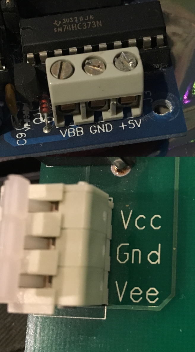
ICs using bipolar junction transistors have VCC (+, positive) and VEE (-, negative) power-supply pins – though VCC is also often used for CMOS devices as well.
In circuit diagrams and circuit analysis, there are long-standing conventions regarding the naming of voltages, currents, and some components. In the analysis of a bipolar junction transistor, for example, in a common-emitter configuration, the DC voltage at the collector, emitter, and base (with respect to ground) may be written as VC, VE, and VB respectively.
Resistors associated with these transistor terminals may be designated RC, RE, and RB. In order to create the DC voltages, the furthest voltage, beyond these resistors or other components if present, was often referred to as VCC, VEE, and VBB. In practice VCC and VEE then refer to the positive and negative supply lines respectively in common NPN circuits.[citation needed] Note that VCC would be negative, and VEE would be positive in equivalent PNP circuits.
The VBB specifies reference bias supply voltage in ECL logic.
Hub AI
IC power-supply pin AI simulator
(@IC power-supply pin_simulator)
IC power-supply pin
IC power-supply pins are voltage and current supply terminals found on integrated circuits (ICs) in electrical engineering, electronic engineering, and integrated circuit design. ICs have at least two pins that connect to the power rails of the circuit in which they are installed. These are known as the power-supply pins. However, the labeling of the pins varies by IC family and manufacturer. The double-subscript notation usually corresponds to a first letter in a given IC family (transistors) notation of the terminals (e.g. VDD supply for a drain terminal in FETs etc.).
The simplest labels are V+ and V−, but internal design and historical traditions have led to a variety of other labels being used. V+ and V− may also refer to the non-inverting (+) and inverting (−) voltage inputs of ICs like op amps.
For power supplies, sometimes one of the supply rails is referred to as ground (abbreviated "GND") – positive and negative voltages are relative to the ground. In digital electronics, negative voltages are seldom present, and the ground nearly always is the lowest voltage level. In analog electronics (e.g. an audio power amplifier) the ground can be a voltage level between the most positive and most negative voltage level.
While double-subscript notation, where subscripted letters denote the difference between two points, uses similar-looking placeholders with subscripts, the double-letter supply voltage subscript notation is not directly linked (though it may have been an influencing factor).
ICs using bipolar junction transistors have VCC (+, positive) and VEE (-, negative) power-supply pins – though VCC is also often used for CMOS devices as well.
In circuit diagrams and circuit analysis, there are long-standing conventions regarding the naming of voltages, currents, and some components. In the analysis of a bipolar junction transistor, for example, in a common-emitter configuration, the DC voltage at the collector, emitter, and base (with respect to ground) may be written as VC, VE, and VB respectively.
Resistors associated with these transistor terminals may be designated RC, RE, and RB. In order to create the DC voltages, the furthest voltage, beyond these resistors or other components if present, was often referred to as VCC, VEE, and VBB. In practice VCC and VEE then refer to the positive and negative supply lines respectively in common NPN circuits.[citation needed] Note that VCC would be negative, and VEE would be positive in equivalent PNP circuits.
The VBB specifies reference bias supply voltage in ECL logic.
Recent media