
Community hub
Recent from talks
Contribute something to knowledge base
Content stats: 0 posts, 0 articles, 1 media, 0 notes
Members stats: 0 subscribers, 0 contributors, 0 moderators, 0 supporters
Subscribers
Supporters
Contributors
Moderators
Hub AI
MOSFET AI simulator
(@MOSFET_simulator)
Hub AI
MOSFET AI simulator
(@MOSFET_simulator)
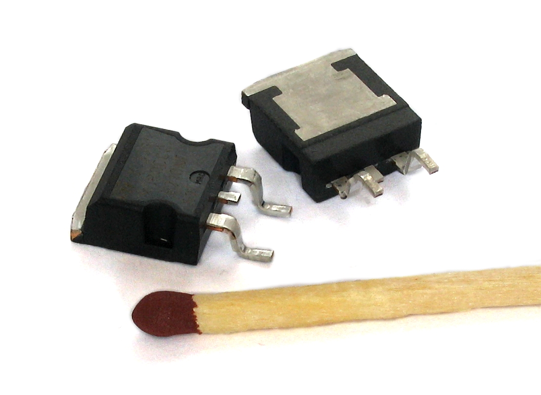
MOSFET
In electronics, the metal–oxide–semiconductor field-effect transistor (MOSFET, MOS-FET, MOS FET, or MOS transistor) is a type of field-effect transistor (FET), most commonly fabricated by the controlled oxidation of silicon. It has an insulated gate, the voltage of which determines the conductivity of the device. This ability to change conductivity with the amount of applied voltage can be used for amplifying or switching electronic signals. The term metal–insulator–semiconductor field-effect transistor (MISFET) is almost synonymous with MOSFET. Another near-synonym is insulated-gate field-effect transistor (IGFET).
The main advantage of a MOSFET is that it requires almost no input current to control the load current under steady-state or low-frequency conditions, especially compared to bipolar junction transistors (BJTs). However, at high frequencies or when switching rapidly, a MOSFET may require significant current to charge and discharge its gate capacitance. In an enhancement mode MOSFET, voltage applied to the gate terminal increases the conductivity of the device. In depletion mode transistors, voltage applied at the gate reduces the conductivity.
The "metal" in the name MOSFET is sometimes a misnomer, because the gate material can be a layer of polysilicon (polycrystalline silicon). Similarly, "oxide" in the name can also be a misnomer, as different dielectric materials are used with the aim of obtaining strong channels with smaller applied voltages.
The MOSFET is by far the most common transistor in digital circuits, as billions may be included in a memory chip or microprocessor. As MOSFETs can be made with either a p-type or n-type channel, complementary pairs of MOS transistors can be used to make switching circuits with very low power consumption, in the form of CMOS logic.
The basic principle of the field-effect transistor was first patented by Julius Edgar Lilienfeld in 1925. In 1934, inventor Oskar Heil independently patented a similar device in Europe.
In the 1940s Bell Labs scientists William Shockley, John Bardeen and Walter Houser Brattain attempted to build a field-effect device which led to their discovery of the transistor effect. However, their structure failed to show the anticipated effects due to the problem of surface states: traps on the semiconductor surface that hold electrons immobile. With no surface passivation they were only able to build the BJT and thyristor transistors.
In 1955, Carl Frosch and Lincoln Derick accidentally grew a layer of silicon dioxide over the silicon wafer, for which they observed surface passivation effects. By 1957 Frosch and Derick, using masking and predeposition, were able to manufacture silicon dioxide field effect transistors; the first planar transistors, in which drain and source were adjacent at the same surface. They showed that silicon dioxide insulated, protected silicon wafers and prevented dopants from diffusing into the wafer. At Bell Labs, the importance of Frosch and Derick technique and transistors was immediately realized. Results of their work circulated around Bell Labs in the form of BTL memos before being published in 1957. At Shockley Semiconductor, Shockley had circulated the preprint of their article in December 1956 to all his senior staff, including Jean Hoerni, who would later invent the planar process in 1959 while at Fairchild Semiconductor.
After this, J.R. Ligenza and W.G. Spitzer studied the mechanism of thermally grown oxides, fabricated a high quality Si/SiO2 stack and published their results in 1960.Following this research, Mohamed Atalla and Dawon Kahng proposed a silicon MOS transistor in 1959 and successfully demonstrated a working MOS device with their Bell Labs team in 1960. Their team included E. E. LaBate and E. I. Povilonis who fabricated the device; M. O. Thurston, L. A. D'Asaro, and J. R. Ligenza who developed the diffusion processes, and H. K. Gummel and R. Lindner who characterized the device. This was a culmination of decades of field-effect research that began with Lilienfeld.
Recent media
Recent media