Recent from talks
Scanning tunneling microscope
Knowledge base stats:
Talk channels stats:
Members stats:
Scanning tunneling microscope
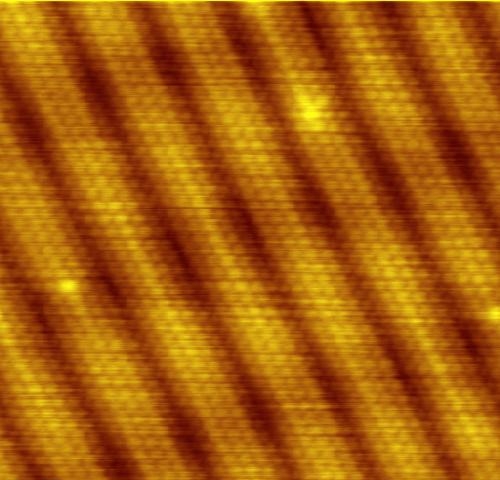
A scanning tunneling microscope (STM) is a type of scanning probe microscope used for imaging surfaces at the atomic level. Its development in 1981 earned its inventors, Gerd Binnig and Heinrich Rohrer, then at IBM Zürich, the Nobel Prize in Physics in 1986. STM senses the surface by using an extremely sharp conducting tip that can distinguish features smaller than 0.1 nm with a 0.01 nm (10 pm) depth resolution. This means that individual atoms can routinely be imaged and manipulated. Most scanning tunneling microscopes are built for use in ultra-high vacuum at temperatures approaching absolute zero, but variants exist for studies in air, water and other environments, and for temperatures over 1000 °C.
STM is based on the concept of quantum tunneling. When the tip is brought very near to the surface to be examined, a bias voltage applied between the two allows electrons to tunnel through the vacuum separating them. The resulting tunneling current is a function of the tip position, applied voltage, and the local density of states (LDOS) of the sample. Information is acquired by monitoring the current as the tip scans across the surface, and is usually displayed in image form.
A refinement of the technique known as scanning tunneling spectroscopy consists of keeping the tip in a constant position above the surface, varying the bias voltage and recording the resultant change in current. Using this technique, the local density of the electronic states can be reconstructed. This is sometimes performed in high magnetic fields and in presence of impurities to infer the properties and interactions of electrons in the studied material, for example from Quasiparticle interference imaging.
Scanning tunneling microscopy can be a challenging technique, as it requires extremely clean and stable surfaces, sharp tips, excellent vibration isolation, and sophisticated electronics. Nonetheless, many hobbyists build their own microscopes.
The tip is brought close to the sample by a coarse positioning mechanism that is usually monitored visually. At close range, fine control of the tip position with respect to the sample surface is achieved by piezoelectric scanner tubes whose length can be altered by a control voltage. A bias voltage is applied between the sample and the tip, and the scanner is gradually elongated until the tip starts receiving the tunneling current. The tip–sample separation w is then kept somewhere in the 4–7 Å (0.4–0.7 nm) range, slightly above the height where the tip would experience repulsive interaction (w < 3 Å), but still in the region where attractive interaction exists (3 < w < 10 Å). The tunneling current, being in the sub-nanoampere range, is amplified as close to the scanner as possible. Once tunneling is established, the sample bias and tip position with respect to the sample are varied according to the requirements of the experiment.
As the tip is moved across the surface in a discrete x–y matrix, the changes in surface height and population of the electronic states cause changes in the tunneling current. Digital images of the surface are formed in one of the two ways: in the constant-height mode changes of the tunneling current are mapped directly, while in the constant-current mode the voltage that controls the height (z) of the tip is recorded while the tunneling current is kept at a predetermined level.
In constant-current mode, feedback electronics adjust the height by a voltage to the piezoelectric height-control mechanism. If at some point the tunneling current is below the set level, the tip is moved towards the sample, and conversely. This mode is relatively slow, as the electronics need to check the tunneling current and adjust the height in a feedback loop at each measured point of the surface. When the surface is atomically flat, the voltage applied to the z-scanner mainly reflects variations in local charge density. But when an atomic step is encountered, or when the surface is buckled due to reconstruction, the height of the scanner also have to change because of the overall topography. The image formed of the z-scanner voltages that were needed to keep the tunneling current constant as the tip scanned the surface thus contain both topographical and electron density data. In some cases it may not be clear whether height changes came as a result of one or the other.
In constant-height mode, the z-scanner voltage is kept constant as the scanner swings back and forth across the surface, and the tunneling current, exponentially dependent on the distance, is mapped. This mode of operation is faster, but on rough surfaces, where there may be large adsorbed molecules present, or ridges and groves, the tip will be in danger of crashing.
Hub AI
Scanning tunneling microscope AI simulator
(@Scanning tunneling microscope_simulator)
Scanning tunneling microscope
A scanning tunneling microscope (STM) is a type of scanning probe microscope used for imaging surfaces at the atomic level. Its development in 1981 earned its inventors, Gerd Binnig and Heinrich Rohrer, then at IBM Zürich, the Nobel Prize in Physics in 1986. STM senses the surface by using an extremely sharp conducting tip that can distinguish features smaller than 0.1 nm with a 0.01 nm (10 pm) depth resolution. This means that individual atoms can routinely be imaged and manipulated. Most scanning tunneling microscopes are built for use in ultra-high vacuum at temperatures approaching absolute zero, but variants exist for studies in air, water and other environments, and for temperatures over 1000 °C.
STM is based on the concept of quantum tunneling. When the tip is brought very near to the surface to be examined, a bias voltage applied between the two allows electrons to tunnel through the vacuum separating them. The resulting tunneling current is a function of the tip position, applied voltage, and the local density of states (LDOS) of the sample. Information is acquired by monitoring the current as the tip scans across the surface, and is usually displayed in image form.
A refinement of the technique known as scanning tunneling spectroscopy consists of keeping the tip in a constant position above the surface, varying the bias voltage and recording the resultant change in current. Using this technique, the local density of the electronic states can be reconstructed. This is sometimes performed in high magnetic fields and in presence of impurities to infer the properties and interactions of electrons in the studied material, for example from Quasiparticle interference imaging.
Scanning tunneling microscopy can be a challenging technique, as it requires extremely clean and stable surfaces, sharp tips, excellent vibration isolation, and sophisticated electronics. Nonetheless, many hobbyists build their own microscopes.
The tip is brought close to the sample by a coarse positioning mechanism that is usually monitored visually. At close range, fine control of the tip position with respect to the sample surface is achieved by piezoelectric scanner tubes whose length can be altered by a control voltage. A bias voltage is applied between the sample and the tip, and the scanner is gradually elongated until the tip starts receiving the tunneling current. The tip–sample separation w is then kept somewhere in the 4–7 Å (0.4–0.7 nm) range, slightly above the height where the tip would experience repulsive interaction (w < 3 Å), but still in the region where attractive interaction exists (3 < w < 10 Å). The tunneling current, being in the sub-nanoampere range, is amplified as close to the scanner as possible. Once tunneling is established, the sample bias and tip position with respect to the sample are varied according to the requirements of the experiment.
As the tip is moved across the surface in a discrete x–y matrix, the changes in surface height and population of the electronic states cause changes in the tunneling current. Digital images of the surface are formed in one of the two ways: in the constant-height mode changes of the tunneling current are mapped directly, while in the constant-current mode the voltage that controls the height (z) of the tip is recorded while the tunneling current is kept at a predetermined level.
In constant-current mode, feedback electronics adjust the height by a voltage to the piezoelectric height-control mechanism. If at some point the tunneling current is below the set level, the tip is moved towards the sample, and conversely. This mode is relatively slow, as the electronics need to check the tunneling current and adjust the height in a feedback loop at each measured point of the surface. When the surface is atomically flat, the voltage applied to the z-scanner mainly reflects variations in local charge density. But when an atomic step is encountered, or when the surface is buckled due to reconstruction, the height of the scanner also have to change because of the overall topography. The image formed of the z-scanner voltages that were needed to keep the tunneling current constant as the tip scanned the surface thus contain both topographical and electron density data. In some cases it may not be clear whether height changes came as a result of one or the other.
In constant-height mode, the z-scanner voltage is kept constant as the scanner swings back and forth across the surface, and the tunneling current, exponentially dependent on the distance, is mapped. This mode of operation is faster, but on rough surfaces, where there may be large adsorbed molecules present, or ridges and groves, the tip will be in danger of crashing.
Recent media