Recent from talks
Unibus
Knowledge base stats:
Talk channels stats:
Members stats:
Unibus
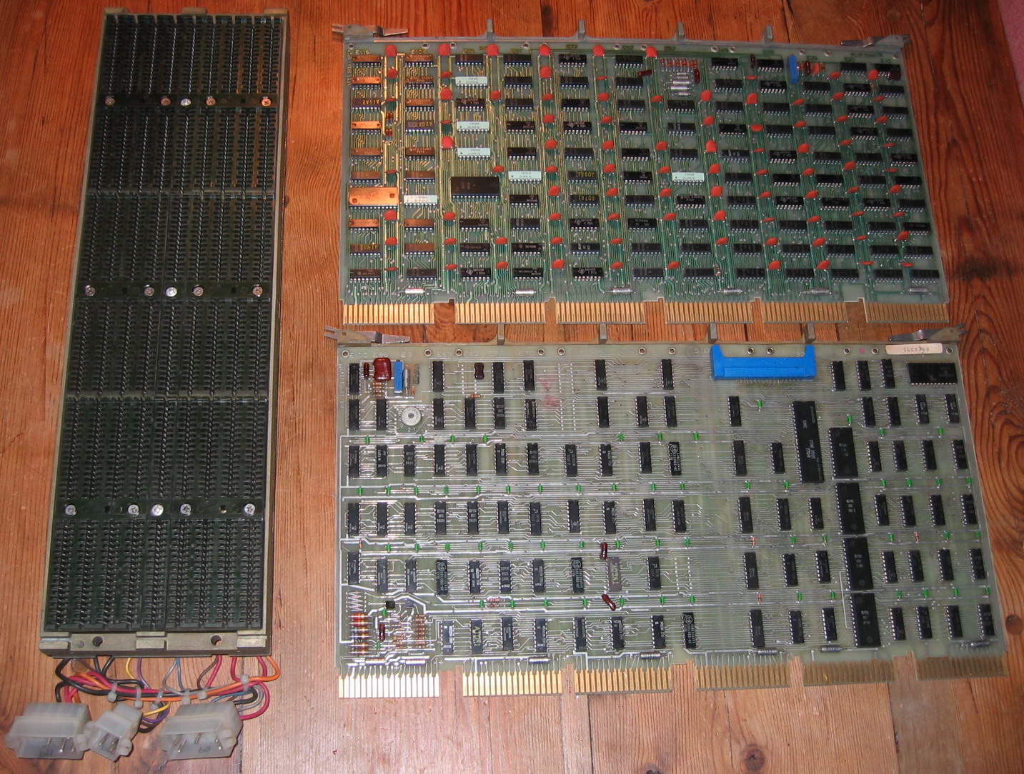
The Unibus was the earliest of several computer bus and backplane designs used with PDP-11 and early VAX systems manufactured by the Digital Equipment Corporation (DEC) of Maynard, Massachusetts. The Unibus was developed around 1969 by Gordon Bell and student Harold McFarland while at Carnegie Mellon University.
The name refers to the unified nature of the bus; Unibus was used both as a system bus allowing the central processing unit to communicate with main memory, as well as a peripheral bus, allowing peripherals to send and receive data. Unifying these formerly separate busses allowed external devices to easily perform direct memory access (DMA) and made the construction of device drivers easier as control and data exchange was all handled through memory-mapped I/O.
Unibus was physically large, which led to the introduction of Q-bus, which multiplexed some signals to reduce pin count. Higher performance PDP systems used Fastbus, essentially two Unibusses in one. The system was later supplanted by Massbus, a dedicated I/O bus introduced on the VAX and late-model PDP-11s.
The Unibus consists of 72 signals, usually connected via two 36-way edge connectors on each printed circuit board. When not counting the power and ground lines, it is usually referred to as a 56-line bus. It can exist within a backplane or on a cable. Up to 20 nodes (devices) can be connected to a single Unibus segment; additional segments can be connected via a bus repeater.
The bus is completely asynchronous, allowing a mixture of fast and slow devices. It allows the overlapping of arbitration (selection of the next bus master) while the current bus master is still performing data transfers. The 18 address lines allow the addressing of a maximum of 256 KB. Typically, the top 8 KB is reserved for the registers of the memory-mapped I/O devices used in the PDP-11 architecture.
The design deliberately minimizes the amount of redundant logic required in the system. For example, a system always contains more slave devices than master devices so most of the complex logic required to implement asynchronous data transfers is forced into the relatively few master devices. For interrupts, only the interrupt-fielding processor needs to contain the complex timing logic. The result is that most I/O controllers can be implemented with simple logic, and most of the critical logic is implemented as a custom MSI IC.
Type 1 lines are a normal multi-sender wired-OR bus with pull-up resistors at each end of the bus, typically on a terminator card.
Type 2 lines are selectively propagated by each card to the next slot – if the card wants to keep the request grant it will assert the SACK line and not propagate the request to the next slot. If a slot is empty, it is necessary to install a "grant continuity card" in the slot to propagate the four type 2 signals to the next card.
Hub AI
Unibus AI simulator
(@Unibus_simulator)
Unibus
The Unibus was the earliest of several computer bus and backplane designs used with PDP-11 and early VAX systems manufactured by the Digital Equipment Corporation (DEC) of Maynard, Massachusetts. The Unibus was developed around 1969 by Gordon Bell and student Harold McFarland while at Carnegie Mellon University.
The name refers to the unified nature of the bus; Unibus was used both as a system bus allowing the central processing unit to communicate with main memory, as well as a peripheral bus, allowing peripherals to send and receive data. Unifying these formerly separate busses allowed external devices to easily perform direct memory access (DMA) and made the construction of device drivers easier as control and data exchange was all handled through memory-mapped I/O.
Unibus was physically large, which led to the introduction of Q-bus, which multiplexed some signals to reduce pin count. Higher performance PDP systems used Fastbus, essentially two Unibusses in one. The system was later supplanted by Massbus, a dedicated I/O bus introduced on the VAX and late-model PDP-11s.
The Unibus consists of 72 signals, usually connected via two 36-way edge connectors on each printed circuit board. When not counting the power and ground lines, it is usually referred to as a 56-line bus. It can exist within a backplane or on a cable. Up to 20 nodes (devices) can be connected to a single Unibus segment; additional segments can be connected via a bus repeater.
The bus is completely asynchronous, allowing a mixture of fast and slow devices. It allows the overlapping of arbitration (selection of the next bus master) while the current bus master is still performing data transfers. The 18 address lines allow the addressing of a maximum of 256 KB. Typically, the top 8 KB is reserved for the registers of the memory-mapped I/O devices used in the PDP-11 architecture.
The design deliberately minimizes the amount of redundant logic required in the system. For example, a system always contains more slave devices than master devices so most of the complex logic required to implement asynchronous data transfers is forced into the relatively few master devices. For interrupts, only the interrupt-fielding processor needs to contain the complex timing logic. The result is that most I/O controllers can be implemented with simple logic, and most of the critical logic is implemented as a custom MSI IC.
Type 1 lines are a normal multi-sender wired-OR bus with pull-up resistors at each end of the bus, typically on a terminator card.
Type 2 lines are selectively propagated by each card to the next slot – if the card wants to keep the request grant it will assert the SACK line and not propagate the request to the next slot. If a slot is empty, it is necessary to install a "grant continuity card" in the slot to propagate the four type 2 signals to the next card.
Recent media