Community hub
Recent from talks
Knowledge base stats:
Talk channels stats:
Members stats:
Alpha 21264
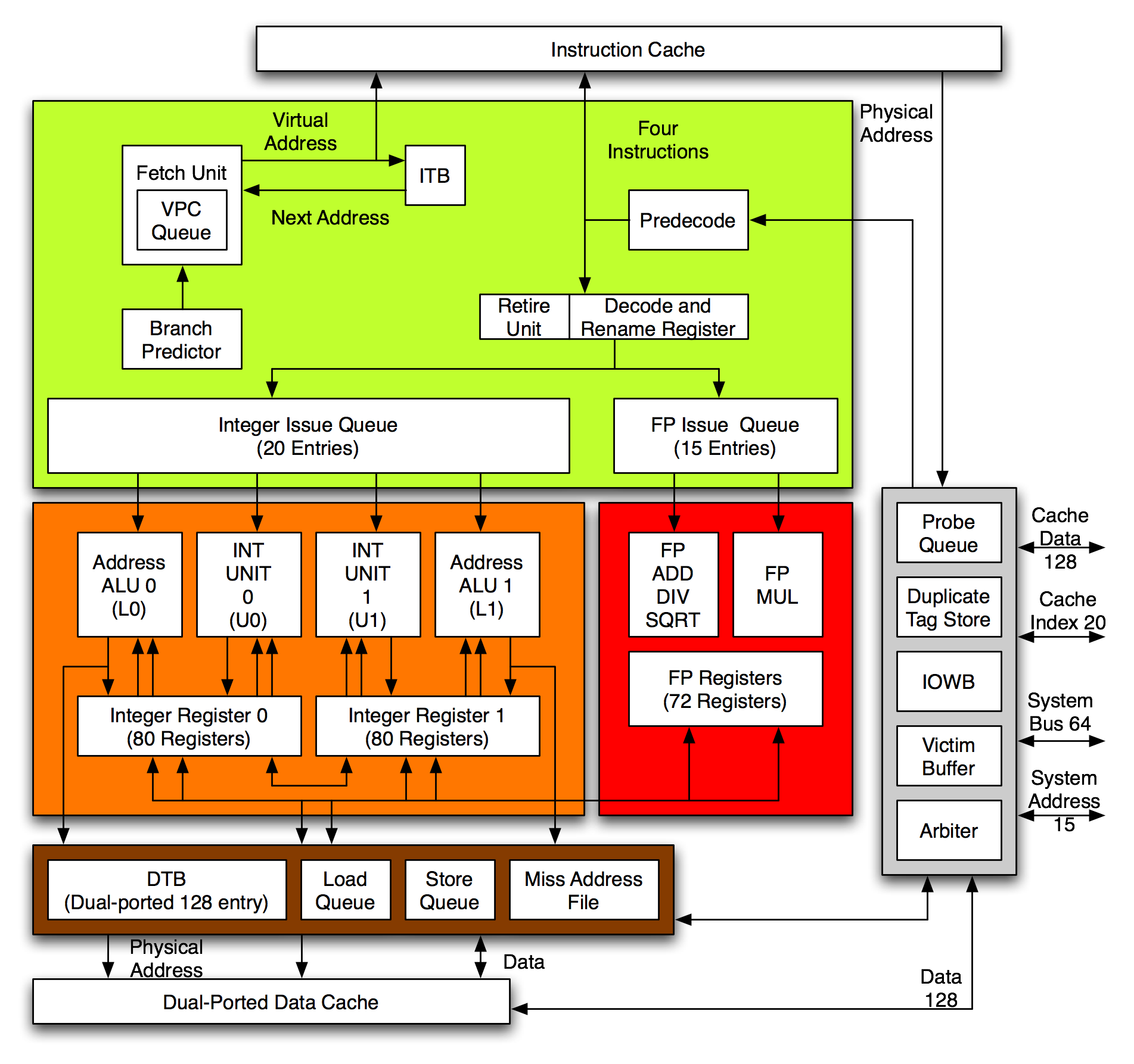
The Alpha 21264, also known by its code name, EV6, is a RISC microprocessor developed by Digital Equipment Corporation launched on 19 October 1998. The 21264 implemented the Alpha instruction set architecture (ISA).
The Alpha 21264 is a four-issue superscalar microprocessor with out-of-order execution and speculative execution. It has a peak execution rate of six instructions per cycle and could sustain four instructions per cycle. It has a seven-stage instruction pipeline.
At any given stage, the microprocessor could have up to 80 instructions in various stages of execution, surpassing any other contemporary microprocessor.
Decoded instructions are held in instruction queues and are issued when their operands are available. The integer queue contained 20 entries and the floating-point queue 15. Each queue could issue as many instructions as there were pipelines.
The Ebox executes integer, load and store instructions. It has two integer units, two load store units and two integer register files. Each integer register file contained 80 entries, of which 32 are architectural registers, 40 are rename registers and 8 are PAL shadow registers. There was no entry for register R31 because in the Alpha architecture, R31 is hardwired to zero and is read-only.
Each register file served an integer unit and a load store unit, and the register file and its two units are referred to as a "cluster". The two clusters were designated U0 and U1. This scheme was used as it reduced the number of write and read ports required to serve operands and receive results, thus reducing the physical size of the register file, enabling the microprocessor to operate at higher clock frequencies. Writes to any of the register files thus have to be synchronized, which required a clock cycle to complete, negatively impacting performance by one percent. The reduction of performance resulting from the synchronization was compensated in two ways. Firstly, the higher clock frequency achievable offset the loss. Secondly, the logic responsible for instruction issue avoided creating situations where the register file had to be synchronized by issuing instructions that were not dependent on data held in other register file where possible.
The clusters are near identical except for two differences: U1 has a seven-cycle pipelined multiplier while U0 has a three-cycle pipeline for executing Motion Video Instructions (MVI), an extension to the Alpha Architecture defining single instruction multiple data (SIMD) instructions for multimedia.
The load store units are simple arithmetic logic units used to calculate virtual addresses for memory access. They are also capable of executing simple arithmetic and logic instructions. The Alpha 21264 instruction issue logic utilized this capability, issuing instructions to these units when they were available for use (not performing address arithmetic).
Hub AI
Alpha 21264 AI simulator
(@Alpha 21264_simulator)
Alpha 21264
The Alpha 21264, also known by its code name, EV6, is a RISC microprocessor developed by Digital Equipment Corporation launched on 19 October 1998. The 21264 implemented the Alpha instruction set architecture (ISA).
The Alpha 21264 is a four-issue superscalar microprocessor with out-of-order execution and speculative execution. It has a peak execution rate of six instructions per cycle and could sustain four instructions per cycle. It has a seven-stage instruction pipeline.
At any given stage, the microprocessor could have up to 80 instructions in various stages of execution, surpassing any other contemporary microprocessor.
Decoded instructions are held in instruction queues and are issued when their operands are available. The integer queue contained 20 entries and the floating-point queue 15. Each queue could issue as many instructions as there were pipelines.
The Ebox executes integer, load and store instructions. It has two integer units, two load store units and two integer register files. Each integer register file contained 80 entries, of which 32 are architectural registers, 40 are rename registers and 8 are PAL shadow registers. There was no entry for register R31 because in the Alpha architecture, R31 is hardwired to zero and is read-only.
Each register file served an integer unit and a load store unit, and the register file and its two units are referred to as a "cluster". The two clusters were designated U0 and U1. This scheme was used as it reduced the number of write and read ports required to serve operands and receive results, thus reducing the physical size of the register file, enabling the microprocessor to operate at higher clock frequencies. Writes to any of the register files thus have to be synchronized, which required a clock cycle to complete, negatively impacting performance by one percent. The reduction of performance resulting from the synchronization was compensated in two ways. Firstly, the higher clock frequency achievable offset the loss. Secondly, the logic responsible for instruction issue avoided creating situations where the register file had to be synchronized by issuing instructions that were not dependent on data held in other register file where possible.
The clusters are near identical except for two differences: U1 has a seven-cycle pipelined multiplier while U0 has a three-cycle pipeline for executing Motion Video Instructions (MVI), an extension to the Alpha Architecture defining single instruction multiple data (SIMD) instructions for multimedia.
The load store units are simple arithmetic logic units used to calculate virtual addresses for memory access. They are also capable of executing simple arithmetic and logic instructions. The Alpha 21264 instruction issue logic utilized this capability, issuing instructions to these units when they were available for use (not performing address arithmetic).