
Community hub
Recent from talks
Contribute something to knowledge base
Content stats: 0 posts, 0 articles, 1 media, 0 notes
Members stats: 0 subscribers, 0 contributors, 0 moderators, 0 supporters
Subscribers
Supporters
Contributors
Moderators
Hub AI
Microfabrication AI simulator
(@Microfabrication_simulator)
Hub AI
Microfabrication AI simulator
(@Microfabrication_simulator)
Microfabrication
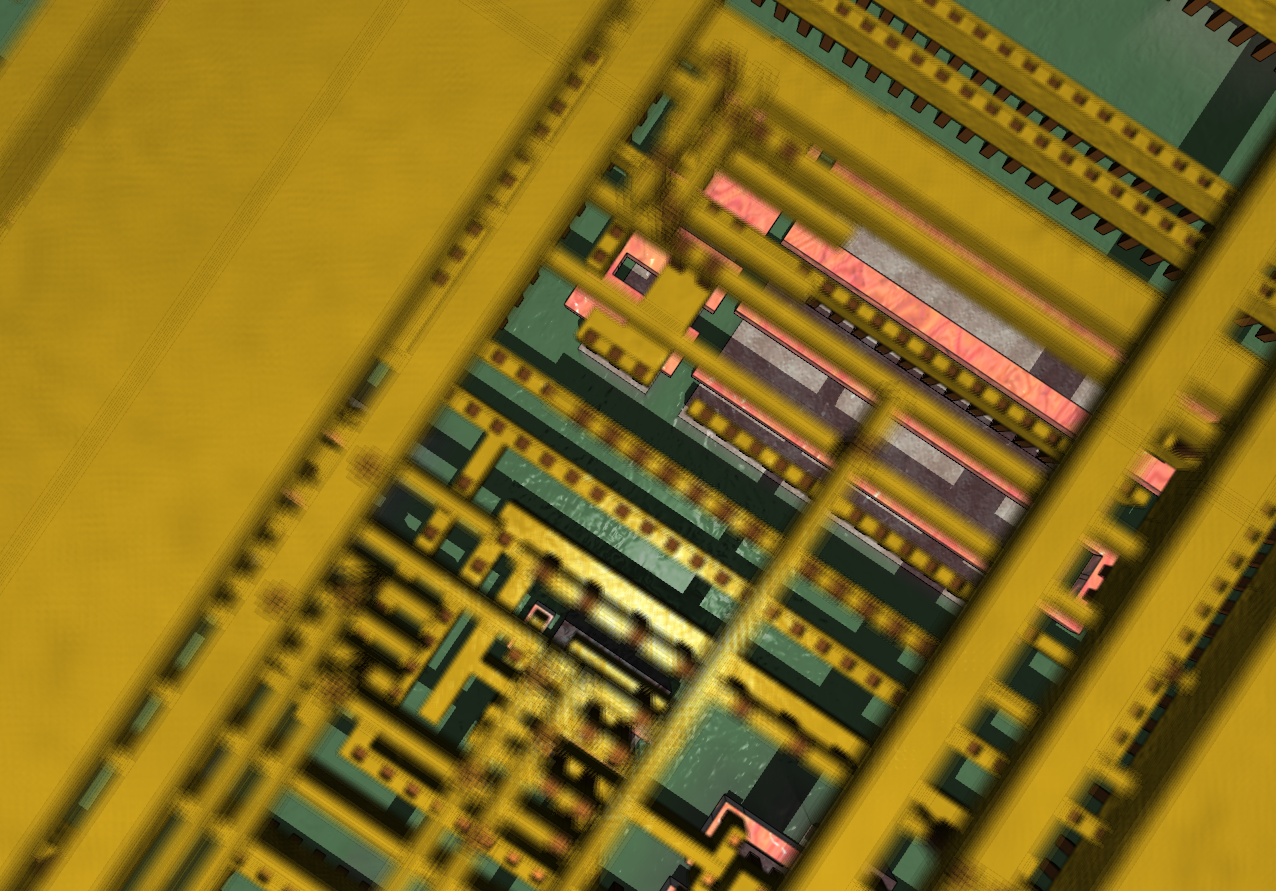
Microfabrication is the process of fabricating miniature structures of micrometre scales and smaller. Historically, the earliest microfabrication processes were used for integrated circuit fabrication, also known as "semiconductor manufacturing" or "semiconductor device fabrication". In the last two decades, microelectromechanical systems (MEMS), microsystems (European usage), micromachines (Japanese terminology) and their subfields have re-used, adapted or extended microfabrication methods. These subfields include microfluidics/lab-on-a-chip, optical MEMS (also called MOEMS), RF MEMS, PowerMEMS, BioMEMS and their extension into nanoscale (for example NEMS, for nano electro mechanical systems). The production of flat-panel displays and solar cells also uses similar techniques.
Miniaturization of various devices presents challenges in many areas of science and engineering: physics, chemistry, materials science, computer science, ultra-precision engineering, fabrication processes, and equipment design. It is also giving rise to various kinds of interdisciplinary research. The major concepts and principles of microfabrication are microlithography, doping, thin films, etching, bonding, and polishing.
Microfabricated devices include:
Microfabrication technologies originate from the microelectronics industry, and the devices are usually made on silicon wafers even though glass, plastics and many other substrate are in use. Micromachining, semiconductor processing, microelectronic fabrication, semiconductor fabrication, MEMS fabrication and integrated circuit technology are terms used instead of microfabrication, but microfabrication is the broad general term.
Traditional machining techniques such as electro-discharge machining, spark erosion machining, and laser drilling have been scaled from the millimeter size range to micrometer range, but they do not share the main idea of microelectronics-originated microfabrication: replication and parallel fabrication of hundreds or millions of identical structures. This parallelism is present in various imprint, casting and moulding techniques which have successfully been applied in the microregime. For example, injection moulding of DVDs involves fabrication of submicrometer-sized spots on the disc.
Microfabrication is actually a collection of technologies which are utilized in making microdevices. Some of them have very old origins, not connected to manufacturing, like lithography or etching. Polishing was borrowed from optics manufacturing, and many of the vacuum techniques come from 19th century physics research. Electroplating is also a 19th-century technique adapted to produce micrometre scale structures, as are various stamping and embossing techniques.
To fabricate a microdevice, many processes must be performed, one after the other, many times repeatedly. These processes typically include depositing a film, patterning the film with the desired micro features, and removing (or etching) portions of the film. Thin film metrology is used typically during each of these individual process steps, to ensure the film structure has the desired characteristics in terms of thickness (t), refractive index (n) and extinction coefficient (k), for suitable device behavior. For example, in memory chip fabrication there are some 30 lithography steps, 10 oxidation steps, 20 etching steps, 10 doping steps, and many others are performed. The complexity of microfabrication processes can be described by their mask count. This is the number of different pattern layers that constitute the final device. Modern microprocessors are made with 30 masks while a few masks suffice for a microfluidic device or a laser diode. Microfabrication resembles multiple exposure photography, with many patterns aligned to each other to create the final structure.
Microfabricated devices are not generally freestanding devices but are usually formed over or in a thicker support substrate. For electronic applications, semiconducting substrates such as silicon wafers can be used. For optical devices or flat panel displays, transparent substrates such as glass or quartz are common. The substrate enables easy handling of the micro device through the many fabrication steps. Often many individual devices are made together on one substrate and then singulated into separated devices toward the end of fabrication.
Microfabrication
Microfabrication is the process of fabricating miniature structures of micrometre scales and smaller. Historically, the earliest microfabrication processes were used for integrated circuit fabrication, also known as "semiconductor manufacturing" or "semiconductor device fabrication". In the last two decades, microelectromechanical systems (MEMS), microsystems (European usage), micromachines (Japanese terminology) and their subfields have re-used, adapted or extended microfabrication methods. These subfields include microfluidics/lab-on-a-chip, optical MEMS (also called MOEMS), RF MEMS, PowerMEMS, BioMEMS and their extension into nanoscale (for example NEMS, for nano electro mechanical systems). The production of flat-panel displays and solar cells also uses similar techniques.
Miniaturization of various devices presents challenges in many areas of science and engineering: physics, chemistry, materials science, computer science, ultra-precision engineering, fabrication processes, and equipment design. It is also giving rise to various kinds of interdisciplinary research. The major concepts and principles of microfabrication are microlithography, doping, thin films, etching, bonding, and polishing.
Microfabricated devices include:
Microfabrication technologies originate from the microelectronics industry, and the devices are usually made on silicon wafers even though glass, plastics and many other substrate are in use. Micromachining, semiconductor processing, microelectronic fabrication, semiconductor fabrication, MEMS fabrication and integrated circuit technology are terms used instead of microfabrication, but microfabrication is the broad general term.
Traditional machining techniques such as electro-discharge machining, spark erosion machining, and laser drilling have been scaled from the millimeter size range to micrometer range, but they do not share the main idea of microelectronics-originated microfabrication: replication and parallel fabrication of hundreds or millions of identical structures. This parallelism is present in various imprint, casting and moulding techniques which have successfully been applied in the microregime. For example, injection moulding of DVDs involves fabrication of submicrometer-sized spots on the disc.
Microfabrication is actually a collection of technologies which are utilized in making microdevices. Some of them have very old origins, not connected to manufacturing, like lithography or etching. Polishing was borrowed from optics manufacturing, and many of the vacuum techniques come from 19th century physics research. Electroplating is also a 19th-century technique adapted to produce micrometre scale structures, as are various stamping and embossing techniques.
To fabricate a microdevice, many processes must be performed, one after the other, many times repeatedly. These processes typically include depositing a film, patterning the film with the desired micro features, and removing (or etching) portions of the film. Thin film metrology is used typically during each of these individual process steps, to ensure the film structure has the desired characteristics in terms of thickness (t), refractive index (n) and extinction coefficient (k), for suitable device behavior. For example, in memory chip fabrication there are some 30 lithography steps, 10 oxidation steps, 20 etching steps, 10 doping steps, and many others are performed. The complexity of microfabrication processes can be described by their mask count. This is the number of different pattern layers that constitute the final device. Modern microprocessors are made with 30 masks while a few masks suffice for a microfluidic device or a laser diode. Microfabrication resembles multiple exposure photography, with many patterns aligned to each other to create the final structure.
Microfabricated devices are not generally freestanding devices but are usually formed over or in a thicker support substrate. For electronic applications, semiconducting substrates such as silicon wafers can be used. For optical devices or flat panel displays, transparent substrates such as glass or quartz are common. The substrate enables easy handling of the micro device through the many fabrication steps. Often many individual devices are made together on one substrate and then singulated into separated devices toward the end of fabrication.
Recent media
Recent media