Hubbry Logo
Precision rectifierPrecision rectifierMain
Open search
Precision rectifier
Community hub
Precision rectifier
logo
7 pages, 0 posts
0 subscribers
Be the first to start a discussion here.
Precision rectifier
Precision rectifier
from Wikipedia

The precision rectifier, sometimes called a super diode, is an operational amplifier (opamp) circuit configuration that behaves like an ideal diode and rectifier.[1]

The op-amp-based precision rectifier should not be confused with the power MOSFET-based active rectification ideal diode.

Basic circuit

[edit]
A simple precision rectifier circuit

The basic circuit implementing such a feature is shown on the right, where can be any load. When the input voltage is negative, the opamp puts its most negative voltage on the diode's anode, so the diode is reverse biased and works like an open circuit. Since almost no current will flow through the diode, the output voltage will be pulled down to ground through . When the input becomes positive, it is amplified by the opamp, which switches the diode on. Because of the negative feedback, just enough current will flow through so that equals the input voltage.

The actual threshold is very close to zero, but is not zero. It equals the actual threshold of the diode, divided by the gain of the opamp.

This basic configuration has a problem, so it is not commonly used. When the input becomes (even slightly) negative, the opamp runs open-loop, as there is no feedback signal through the diode. For a typical opamp with high open-loop gain, the output saturates. If the input then becomes positive again, the op-amp has to get out of the saturated state before positive amplification can take place again. This change generates some ringing and takes some time, greatly reducing the frequency response of the circuit.

Improved circuit

[edit]
An improved precision rectifier circuit.

An alternative version is given on the right. In this case, when the input is greater than zero, D1 is off, and D2 is on, so the output is zero because the other end of is connected to the virtual ground and there is no current through . When the input is less than zero, D1 is on and D2 is off, so the output is like the input with an amplification of . Its input–output relationship is the following:

Super diode improved

This circuit has the benefit that the op-amp never goes into saturation, but its output must change by two diode voltage drops (about 1.2 V) each time the input signal crosses zero. Hence, the slew rate of the opamp and its frequency response (gain–bandwidth product) will limit high-frequency performance, especially for low signal levels, although an error of less than 1% at 100 kHz is possible.

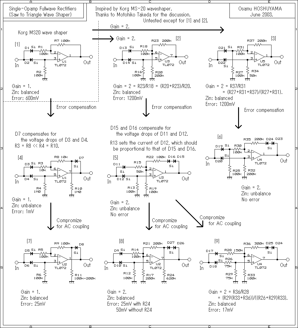
Similar circuitry can be used to create a precision full-wave rectifier circuit.

Peak detector

[edit]

With a little modification, the basic precision rectifier can be used for detecting signal level peaks. In the following circuit, a capacitor retains the peak voltage level of the signal, and a switch is used for resetting the detected level. When the input Vin exceeds Vc (voltage across capacitor), the diode is forward-biased and the circuit becomes a voltage follower. Consequently, the output voltage Vo follows Vin as long as Vin exceeds Vc. When Vin drops below Vc, the diode becomes reverse-biased and the capacitor holds the charge until Vin again attains a value greater than Vc.

Peak detector
Peak detector

References

[edit]
[edit]
Revisions and contributorsEdit on WikipediaRead on Wikipedia
from Grokipedia
A precision rectifier is an electronic circuit that employs operational amplifiers (op-amps) and diodes to accurately rectify alternating current (AC) signals into direct current (DC), particularly for low-amplitude inputs where conventional diode rectifiers fail due to the diodes' forward voltage drop of approximately 0.7 V. This design leverages the op-amp's virtual ground principle to bias the diodes, ensuring the output closely follows the absolute value of the input signal without distortion from threshold losses. Precision rectifiers are essential in applications requiring , as they enable rectification of signals as small as 50 mV peak-to-peak up to frequencies around 1 kHz with minimal (THD). Unlike passive circuits, which distort small signals by clipping below the diode's turn-on voltage, precision versions use active feedback to maintain and high . Key components typically include low-noise op-amps (e.g., OPA2211 or OP484), fast-switching diodes (e.g., 1N4148 or 1N914), and precision resistors for gain control. Common configurations include the half-wave precision rectifier, which processes only one polarity of the input (e.g., positive half-cycles) using a single op-amp and in a "superdiode" arrangement, and the full-wave precision rectifier, which captures both polarities to produce an output, often combining an inverting half-wave stage with a summing . Full-wave designs, such as those operating on dual supplies, can handle inputs up to 20 V peak-to-peak at 50 kHz while preserving . These circuits may incorporate filtering—high-pass to remove DC offsets and low-pass for smoothing—to enhance usability in measurement systems. Applications of precision rectifiers span amplitude detection, envelope extraction in AM demodulation, absolute value computation in digital signal processing, and instrumentation for quantifying AC signal magnitudes in low-voltage environments. Their precision makes them valuable in educational labs, audio processing, and sensor interfaces where accurate waveform shaping is critical.

Overview

Definition and Purpose

A precision rectifier, often referred to as a super diode, is an configuration that employs an to replicate the characteristics of an ideal , allowing current to flow with zero forward during forward bias while providing complete blocking in reverse bias. This design addresses the inherent limitations of conventional s by leveraging the high gain and low offset voltage of the op-amp to achieve near-ideal rectification performance. The primary purpose of a precision rectifier is to enable accurate rectification of low-amplitude signals, especially those below the 0.7 V forward voltage threshold of standard silicon diodes, which would otherwise result in significant or failure to conduct in passive rectifier circuits. It finds essential use in tasks requiring precise waveform shaping, instrumentation systems for measurement accuracy, and low-voltage environments where conventional rectification proves inadequate. At its core, the basic block diagram of a precision rectifier features an with a integrated into the feedback loop, where the op-amp actively compensates for the 's characteristics to maintain linear operation across the input signal range.

Advantages Over Conventional Rectifiers

Precision rectifiers overcome the inherent limitations of conventional diode-based rectifiers by incorporating to eliminate the 's forward of approximately 0.6 to 0.7 V, allowing accurate rectification of low-amplitude AC signals down to the millivolt level that would otherwise be clipped or unattainable with passive . This design ensures that signals as small as 0.1 V are rectified with minimal distortion, providing outputs that closely follow the input without the threshold barrier imposed by characteristics. The use of an op-amp in the feedback loop imparts high , typically in the megaohm range, and low output , as the buffering action isolates the input signal from loading effects and maintains across the operational range. Unlike conventional rectifiers, where non-idealities introduce significant , precision versions achieve very low for signals within the op-amp's capabilities, enhancing signal in applications requiring clean rectification. Precision rectifiers exhibit greater temperature independence compared to conventional designs, where the forward voltage varies by about -2 mV/°C, leading to output drift; op-amp compensation mechanisms reduce this sensitivity, maintaining stable performance over temperature variations. This stability is particularly beneficial in environments with fluctuating temperatures, as the circuit's output remains consistent without the need for additional compensation components. In terms of accuracy, conventional diode rectifiers suffer errors of 10-20% or more for low-level signals due to the , whereas precision rectifiers reduce this to less than 1%, enabling precise even at amplitudes below 100 mV. Additionally, precision rectifiers extend operational bandwidth to the op-amp's gain-bandwidth product, often reaching 1-10 MHz depending on the device, far surpassing the frequency limitations of simple diode circuits constrained by recovery times and capacitance effects. This allows for rectification of higher-frequency signals while preserving accuracy, making them suitable for modern tasks.

Fundamental Principles

Limitations of Diode-Based Rectifiers

Diode-based rectifiers, relying on passive junctions, suffer from a significant forward during conduction, typically around 0.7 V for diodes and 0.3 V for Schottky types, which subtracts from the input signal and causes substantial or complete loss for low-amplitude inputs below 1 V. This threshold behavior results in the rectifier failing to conduct until the input exceeds the drop, leading to clipped or absent output for small signals, such as in precision where accurate rectification of millivolt-level waveforms is required. Additionally, in the non-conducting phase allows a small but non-negligible flow of current, typically in the microampere range, which degrades blocking during the opposite polarity cycle and introduces errors in the rectified output. This leakage arises from minority carrier in the and becomes more pronounced at higher temperatures, further compromising isolation in half-wave or full-wave configurations. The forward exhibits a , decreasing by approximately 2 mV per degree for diodes, which causes output drift and instability across varying environmental conditions. This thermal sensitivity exacerbates nonlinearity inherent to the diode's exponential current-voltage characteristic, producing harmonic distortion and crossover effects in half-wave and full-wave setups where the transition between conducting and blocking states introduces waveform irregularities. For instance, applying a 100 mV sine wave to a conventional silicon diode rectifier yields nearly zero output, as the signal never surpasses the 0.7 V threshold, rendering the circuit ineffective for low-level applications. These limitations highlight the need for active precision rectifiers to achieve accurate low-voltage rectification without such offsets and distortions.

Operational Amplifier in Precision Rectification

In precision rectification, the operational amplifier (op-amp) employs the virtual ground principle, where negative feedback maintains the inverting input terminal at approximately zero volts relative to ground. This configuration ensures that the diode, typically placed in the feedback path, is forward-biased during conduction, with the op-amp compensating for its forward voltage drop to enable precise and immediate response to input signals without the threshold delays inherent in passive diodes. The feedback loop dynamics are central to the op-amp's role, as the diode in the feedback path enables the op-amp to dynamically adjust its output voltage. When the input signal forward-biases the diode, the op-amp increases its output to compensate exactly for the diode's forward (Vf, typically 0.6-0.7 V), effectively making the diode behave as an ideal element that conducts with negligible loss. This compensation arises because the feedback signal is derived after the diode, allowing the op-amp's high loop gain to minimize errors and transfer the input voltage directly to the output. Under ideal op-amp assumptions, including infinite and zero , the circuit achieves perfect rectification in the forward bias region. For a unity gain configuration, the output voltage is an inverted version of the input for the conducting half-cycle, given by the equation: Vout=VinV_{out} = -V_{in} This relation holds because the infinite gain forces the differential input voltage to zero, ensuring the and ideal action without or offset. Practical implementation requires attention to the op-amp's and bandwidth as key prerequisites for performance. The , which measures the maximum rate of output voltage change (typically in V/µs), limits the circuit's response to rapid signal transitions, such as zero crossings, potentially causing if the input frequency exceeds the op-amp's capabilities (e.g., below 10 kHz for standard op-amps with low-level signals). Similarly, the gain-bandwidth product determines the operational frequency range, necessitating selection of op-amps with sufficient bandwidth to maintain accuracy across the desired signal spectrum.

Circuit Configurations

Basic Half-Wave Precision Rectifier

The basic half-wave precision rectifier is the simplest configuration employing an (op-amp) to achieve accurate rectification of positive input half-cycles, overcoming the forward limitations of conventional rectifiers. The consists of an op-amp with the input signal connected to the non-inverting terminal, the inverting terminal connected to the of a whose is connected to the op-amp output, and the output voltage VoutV_{out} taken from the inverting terminal ( of the ). During operation with a positive input voltage Vin>0V_{in} > 0, the op-amp drives its output positive to maintain at the inverting input via through the conducting , which is forward-biased. This feedback loop compensates for the 's forward (typically 0.6–0.7 V), ensuring the effective output follows the input without offset. For a unity-gain setup, the relationship yields Vout=VinV_{out} = V_{in}. In contrast, for Vin<0V_{in} < 0, the becomes reverse-biased, opening the feedback loop and causing the op-amp output to saturate at the negative supply rail (e.g., -12 V or lower, depending on the supply), resulting in Vout=0V_{out} = 0 V as the inverting input is pulled to ground through the load. The ideal transfer characteristic can be expressed as: Vout={VinVin>00Vin<0V_{out} = \begin{cases} V_{in} & V_{in} > 0 \\ 0 & V_{in} < 0 \end{cases} This rectifies only the positive half-cycle, blocking the negative portion. A key drawback arises during negative inputs, where the absence of feedback causes the op-amp to saturate, leading to output distortion and a recovery time limited by the op-amp's slew rate (e.g., approximately 26 µs for a common 741 op-amp), which restricts the circuit's usable frequency range to low values. The op-amp's brief mention of negative feedback principles underscores how the closed-loop operation during positive cycles enforces precision, but the open-loop saturation for negatives highlights the need for careful component selection to minimize distortion. The transfer characteristic graph plots VoutV_{out} versus VinV_{in}, showing a straight line with unity slope passing through the origin for positive VinV_{in}, transitioning sharply to the horizontal axis ( Vout=0V_{out} = 0 ) for negative VinV_{in}, forming an ideal half-wave rectified without the threshold offset seen in simple circuits. In practice, minor deviations occur near due to saturation recovery and finite .

Improved Precision Rectifier

The improved precision rectifier enhances the basic design by incorporating an additional diode and resistor to limit the op-amp output swing during non-conducting cycles, preventing it from reaching the negative supply rail. This modification maintains the feedback loop's integrity and reduces recovery time from saturation. When the input voltage VinV_{in} is positive, the feedback diode conducts, and the circuit functions similarly to the basic inverting amplifier, producing an output that precisely follows the inverted input without the forward voltage drop inherent in conventional diodes. For negative VinV_{in}, the additional diode and resistor redirect the path, keeping the op-amp in its linear region by limiting the output swing and providing an alternative feedback route. This results in improved linearity for low-amplitude signals, such as 2 mV peak, with dramatically reduced distortion compared to the basic circuit. The gain is adjustable via the resistor ratio in the feedback network (typically unity gain for Rf/Rin=1R_f / R_{in} = 1). This configuration significantly reduces and improves response time relative to the basic precision rectifier. It also demonstrates superior accuracy for low-amplitude signals. Unlike the basic half-wave precision rectifier, where negative inputs cause op-amp saturation and prolonged recovery delays, the improved version's and addition resolve this issue in a single stage, enabling better performance without requiring multiple op-amps.

Full-Wave Precision Rectifier

The full-wave precision rectifier is an that converts an (AC) input signal into a unidirectional pulsating (DC) output by rectifying both the positive and negative half-cycles of the input waveform, producing an output voltage that follows the of the input. This configuration typically employs two operational amplifiers (op-amps) along with and resistors to achieve precise rectification without the forward inherent in conventional diode bridges. It is particularly useful in applications requiring accurate full-cycle conversion, such as AC-to-DC conversion in . One common schematic implementation consists of two precision half-wave stages: an inverting half-wave rectifier followed by a summing that combines the signals to yield the full-wave output. In this setup, the first op-amp (A1) with associated diodes and resistors processes the input to pass the negative half-cycle inverted to positive while blocking the positive half-cycle, and the second op-amp (A2) acts as a unity-gain summer that adds the original positive half-cycle (passed through a buffer) with the inverted negative half-cycle. An alternative configuration uses an op-amp bridge with four diodes arranged to direct both polarities through appropriate paths, though the two-op-amp approach is more prevalent for its simplicity and precision. During operation, for a positive input cycle, the first (D1) is reverse-biased, allowing the signal to pass unattenuated through the non-inverting path to the summing stage, while the second (D2) is forward-biased to shunt the inverted path to ground; this results in the output following the input directly. For a negative input cycle, D1 becomes forward-biased, enabling the first op-amp to invert the signal (with unity gain via equal resistors), while D2 reverse-biases to block the direct path, ensuring the output remains positive. The op-amps maintain at their inputs, compensating for drops and enabling rectification of signals as low as 50 mV peak-to-peak with minimal up to 50 kHz. Building on half-wave precision rectifier principles, this dual-stage approach ensures both cycles contribute to the output without phase inversion relative to the input's . The ideal transfer characteristic is given by the equation: Vout=VinV_{out} = |V_{in}| where the gain is unity, though adjustable via resistor ratios (e.g., Vout=GVinV_{out} = G |V_{in}| with G=Rf/RinG = R_f / R_{in}) for amplification needs. This equation holds across the full input range, such as ±10 V, without the 0.7 V offset of silicon diodes. Advantages of the full-wave precision rectifier include a smoother DC output compared to half-wave designs due to utilization of both input cycles, leading to higher average output voltage and reduced ripple for efficient AC-to-DC conversion. It provides superior accuracy for low-amplitude signals by eliminating diode threshold losses, with distortion below 1% and fast recovery from overloads, making it ideal for precision measurement systems. Additionally, the circuit offers high input impedance and low output distortion, enhancing efficiency in power-sensitive applications. Variants include dual-supply implementations, which use symmetric supplies (e.g., ±15 V) for balanced operation across bipolar inputs and outputs, ensuring over a wide range without offset adjustments. Single-supply versions adapt the circuit by incorporating level-shifting resistors or diodes to reference the output to a positive rail (e.g., 0 to 5 V from a +5 V supply), suitable for battery-powered devices, though they may require careful op-amp selection to maintain precision.

Applications

Peak Detector

A peak detector based on a precision rectifier captures and holds the maximum of an input signal by integrating the rectified output with a storage element. The circuit typically consists of a precision half-wave or full-wave rectifier stage whose output feeds into a parallel RC network, where a directs the rectified signal to charge a , and a provides a controlled discharge path. This configuration ensures that the charges rapidly to the peak voltage during each cycle of the input signal and holds that value until intentionally discharged, with the precision rectifier compensating for forward voltage drops to maintain accuracy even for low- signals. In operation, when the input signal exceeds the voltage across the , the delivers a positive output that forward-biases the holding , allowing the low-impedance path from the op-amp to charge the to the input peak value. Once the input falls below this peak, the reverse-biases, isolating the and preventing discharge through the ; the stored voltage is then maintained at the output, typically buffered by a unity-gain op-amp to avoid loading effects. The precision nature of the ensures that the forward VfV_f is effectively zero due to op-amp feedback, yielding an output peak voltage VpeakVmax(input)V_{peak} \approx V_{max(input)}, which is particularly accurate for signals as low as a few millivolts. The discharge occurs exponentially through the parallel with a τ=RC\tau = RC, allowing the hold time to be tuned by selecting appropriate component values—typically much longer than the input signal period for stable peak retention. These circuits find applications in analog-to-digital converters (ADCs) for sample-and-hold peak measurement and in envelope detection for amplitude-modulated signals, where they provide high accuracy for input signals exceeding 10 mV at low frequencies. The droop rate, or gradual voltage loss during the hold period due to capacitor leakage and resistor discharge, is minimized by using high-value resistors (e.g., in the megaohm range) and low-leakage diodes or capacitors, ensuring the output remains close to the true peak for hold times on the order of milliseconds to seconds.

Absolute Value and Clamping Circuits

The absolute value circuit, a specialized variant of the improved precision rectifier, produces a continuous output equal to the magnitude of the input signal, |V_in|, without inversion. This configuration typically employs two operational amplifiers and precision resistors to ensure high and accurate rectification for both positive and negative inputs. In the standard , the first op-amp (A1) acts as a buffer or inverter depending on the input polarity, directing the signal through diodes to the second op-amp (A2), which provides non-inverted amplification via a network (e.g., R1 and R2 set equal for unity gain). For positive inputs, the signal passes directly; for negative inputs, it is inverted twice to yield the positive magnitude, enabling seamless full-wave operation. The output voltage follows the relation: Vout=GVinV_{out} = G |V_{in}| where GG is the gain determined by the resistor ratio (e.g., G=1G = 1 if R1 = R2). This design overcomes the limitations of diode-only circuits by compensating for the forward voltage drop, allowing precise handling of low-amplitude bipolar signals down to millivolts. In clamping applications, a precision rectifier configuration uses an op-amp with a diode in the feedback loop—often termed a "superdiode"—to limit signal excursions above or below predefined thresholds without introducing distortion from the diode's voltage drop. The op-amp drives the diode to maintain virtual ground at the input, clamping the output to a reference voltage (V_ref) while preserving waveform shape for signals exceeding the threshold; for instance, a capacitor may couple the input to shift DC levels precisely. This diode-op-amp combination achieves far superior accuracy to passive diode clamps for low-level signals. These circuits find specific use in audio processing for full-wave folding, where the function converts bipolar audio signals to unipolar for effects like harmonic distortion generation, ensuring clean rectification without crossover glitches. In sensor protection, clamping variants safeguard systems by limiting overvoltages (e.g., transients up to 5 kV) to safe levels like 2.5 , with settling times around 100 ns, preventing damage while maintaining for bipolar sensor outputs. Unlike peak detectors, which transient maxima using capacitors, absolute value and clamping circuits provide real-time, continuous waveform shaping without storage elements.

Design Considerations

Op-Amp Selection and Requirements

Selecting an (op-amp) for precision rectifier circuits requires careful consideration of specifications that ensure accurate signal rectification, particularly at low voltages and high frequencies. Key parameters include low , typically less than 1 mV, to minimize DC errors during zero-crossing detection; a high , exceeding 1 V/μs, to handle rapid signal transitions without ; wide unity-gain bandwidth, greater than 1 MHz, for faithful reproduction of the input ; and low , such as voltage noise density below 10 nV/√Hz, to preserve in low-level applications. Supply voltage requirements depend on the circuit's operating range: dual supplies, such as ±15 , are preferred for full in bipolar signals, while rail-to-rail input and output op-amps enable single-supply operation (e.g., 5 ) for portable designs. The input common-mode voltage range must include ground (0 ) to accurately detect zero crossings without phase errors or . Suitable op-amp examples include the OP07 from , valued for its low offset voltage (as low as 25 μV) in precision applications, and the TL081 from , a general-purpose JFET-input with adequate bandwidth (3 MHz) and (13 V/μs) for moderate-frequency rectification. Comparators should be avoided, as they lack the essential for linear operation in rectifiers. For battery-powered applications, power consumption trade-offs are critical; op-amps with low quiescent current, such as 1 mA per channel (e.g., OPA197), balance precision with extended battery life, whereas higher-performance devices like the OPA2211 (3.8 mA quiescent current) offer superior (27 V/μs) and (1.1 nV/√Hz) at the cost of increased power draw.

Non-Ideal Effects and Mitigation

In precision rectifiers, the of the introduces a DC shift in the output, leading to inaccuracies in the rectified , particularly for low-amplitude signals. This error arises because the offset voltage acts as an unintended differential input, causing the op-amp to produce a non-zero output even when the input is zero. To mitigate this, auto-zero or chopper-stabilized op-amps can be employed, which periodically sample and cancel the offset, achieving offsets as low as 3 µV maximum, or external trimming circuits can adjust the offset to near zero with input shorted. Slew rate limitations in the op-amp distort fast signal edges during transitions, resulting in rounded corners or clipping in the rectified output, especially at higher frequencies. The time required for the op-amp output to swing sufficiently to forward-bias the is determined by the , limiting the circuit's ability to track rapid changes accurately. Mitigation involves selecting op-amps with high , such as 10 V/µs or greater, and adding compensation capacitors to stabilize the feedback loop and reduce overshoot. The finite and bandwidth of the op-amp cause a in performance at higher frequencies, introducing gain errors in the rectified signal. The relative error can be approximated as ϵ1Aol\epsilon \approx \frac{1}{A_{ol}}, where AolA_{ol} is the , leading to deviations on the order of 100 ppm for typical gains of 20,000. This effect is exacerbated near the unity-gain bandwidth, reducing loop gain and precision. To counteract it, op-amps with high gain-bandwidth products (e.g., over 1 MHz) and low phase lag are chosen, ensuring the loop gain remains sufficient for the operating frequency. Diode reverse recovery time adds a delay during signal polarity reversal, causing brief conduction in the reverse direction and distorting the output with spikes or dead time. This stored charge in the must dissipate before blocking, typically on the order of nanoseconds. Using fast-recovery diodes, such as the 1N4148 with a reverse recovery time of about 4 ns, minimizes this delay and improves switching speed in precision applications. In designs from the 2020s, CMOS-based op-amps enable lower power consumption (e.g., 250 µA quiescent current) for battery-operated precision rectifiers but often exhibit higher input offsets (up to 25 µV) compared to bipolar counterparts due to process variations. These advancements prioritize zero-drift architectures to maintain precision in low-power scenarios.

References

Add your contribution
Related Hubs
User Avatar
No comments yet.