Hubbry Logo
Video random-access memoryVideo random-access memoryMain
Open search
Video random-access memory
Community hub
Video random-access memory
logo
8 pages, 0 posts
0 subscribers
Be the first to start a discussion here.
Video random-access memory
from Wikipedia
GDDR5X SDRAM on an NVIDIA GeForce GTX 1080 Ti graphics card

Video random-access memory (VRAM) is dedicated computer memory used to store the pixels and other graphics data as a framebuffer to be rendered on a computer monitor.[1] It often uses a different technology than other computer memory, in order to be read quickly for display on a screen.

Relation to GPUs

[edit]
Independent system RAM and video RAM
Unified memory
A GPU die surrounded by VRAM chips

Many modern GPUs rely on VRAM. In contrast, a GPU that does not use VRAM, and relies instead on system RAM, is said to have a unified memory architecture, or shared graphics memory.

System RAM and VRAM have been segregated due to the bandwidth requirements of GPUs,[2][3] and to achieve lower latency, since VRAM is physically closer to the GPU die.[4]

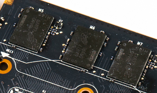
Modern VRAM is typically found in a BGA package[5] soldered onto a graphics card.[6] The VRAM is cooled along with the GPU by the GPU heatsink.[7]

Technologies

[edit]

See also

[edit]

References

[edit]
Revisions and contributorsEdit on WikipediaRead on Wikipedia
from Grokipedia
Video random-access memory (VRAM) is a specialized type of dual-ported (DRAM) designed for use in cards and other display systems, where it stores data, textures, and frame buffers to facilitate rapid rendering and output of visual content to a display. Unlike standard system RAM, VRAM's dual-port architecture allows simultaneous access—one port for the graphics processor to write or update data, and the other for continuously refreshing the display output—thereby doubling bandwidth and reducing latency in video operations. Invented in 1980 by researchers Frederick Dill, Daniel Ling, and Richard Matick, VRAM was patented in 1985 as a solution to accelerate in computing systems. Originally implemented as dual-ported DRAM chips, VRAM evolved through variants like synchronous graphics RAM (SGRAM), which added features for 3D acceleration such as block writes for efficient , and window RAM (WRAM), a high-bandwidth dual-ported successor offering about 25% more throughput than early VRAM at lower cost. By the late and into the , VRAM transitioned to faster synchronous DRAM derivatives, including (DDR) technologies like GDDR3, GDDR4, GDDR6, and the current standards GDDR6X and GDDR7, which use high-speed interfaces and wider memory buses (e.g., 256-bit or 384-bit) to handle the demands of high-resolution gaming, video editing, and AI workloads. Modern GPUs integrate VRAM capacities ranging from 8 GB to 24 GB or more in consumer cards, with high-bandwidth memory (HBM) variants such as HBM3 in professional and data center cards providing up to 141 GB for even greater parallelism and efficiency in data-intensive applications. The amount and speed of VRAM directly impact graphical performance; for instance, at least 8 GB is recommended for gaming at high settings as of 2025, while 16 GB or higher supports 4K resolutions and multi-monitor setups without stuttering.

Fundamentals

Definition and Purpose

Video random-access memory (VRAM) is a dual-ported variant of (DRAM) optimized for high-performance video display tasks, setting it apart from general-purpose system RAM that serves broader computing needs. This specialization allows VRAM to handle the intensive demands of graphics processing without interfering with system-wide memory operations. The core purpose of VRAM is to maintain a —a dedicated buffer that stores data essential for rendering images, including color components, depth buffers for 3D scenes, and texture maps used in visual computations. By holding this data in close proximity to the hardware, VRAM facilitates efficient real-time generation of visual content for output to monitors or other displays. VRAM's supports simultaneous high-speed read and write operations, enabling the processor to update the with incoming frame data while the display controller accesses the existing content to generate continuous video signals. In contemporary cards, VRAM capacities generally span from 4 GB in entry-level configurations to 32 GB or higher in advanced models, ensuring it remains exclusively allocated for workloads, as of late 2025.

Basic Operation

Video random-access memory (VRAM) operates by allowing the (GPU) to write pixel data to its random-access port while the concurrently reads data for display refresh. This workflow ensures that the GPU can continuously update image data without halting the output to the display, which typically refreshes at rates such as 60 Hz to maintain smooth visuals. At the core of this process is the , a dedicated region in VRAM structured as a two-dimensional array corresponding to the , where each element represents a and stores color values in RGB format. Additional buffers, such as the Z-buffer, may reside alongside the color buffer to hold depth information for hidden surface removal in , enabling efficient management of complex scenes. Refresh cycles in VRAM involve the serial access memory (SAM) registers loading frame data from the main DRAM array and clocking it out sequentially to the display controller, providing uninterrupted scanning of the entire . This mechanism prevents display flicker and supports real-time rendering by decoupling read operations from GPU write activities. The facilitates high-resolution displays up to 8K (7680 × 4320 s) and beyond, with pixel bit depths ranging from 24 to 32 bits to deliver rich color fidelity in modern applications.

History

Origins and Invention

Video random-access memory (VRAM) was invented in 1980 by IBM researchers Frederick H. Dill, Daniel T. Ling, and Richard E. Matick at the IBM Thomas J. Watson Research Center. The motivation stemmed from the need to address performance bottlenecks in professional graphics workstations, where single-ported dynamic random-access memory (DRAM) could not efficiently handle simultaneous random accesses from the CPU or graphics processor and high-bandwidth serial readouts required for video display refresh. This dual-port architecture allowed the primary port to support conventional random access while a secondary asynchronous port enabled block transfers, such as serial output for CRT displays, without contention. The invention was patented in 1985 as U.S. Patent 4,541,075, describing a semiconductor RAM with an integrated row buffer—exemplified as 256 bits wide in a 256×256 organization—for parallel data shifting to the secondary port. The first VRAM chips were 64K × 4 multibank DRAMs featuring a 256-bit serial access port designed to match the video bandwidth demands of early high-resolution displays. These chips represented a specialized evolution of DRAM, incorporating a static serial access memory (SAM) shift register to facilitate continuous video streaming. The first commercial implementation of VRAM appeared in within a high-resolution graphics adapter for IBM's RT PC workstation, enabling advanced graphics capabilities in and scientific applications. By 1987, VRAM was integrated into IBM's 8514 graphics adapter for the PS/2 line, supporting 1024×768 resolution with up to 256 colors from a palette, primarily for (CAD) and professional visualization tasks. This early adoption marked VRAM's role in transitioning from to color workstations, providing the necessary for smooth display updates.

Key Milestones and Evolution

In the early , the development of specialized VRAM variants marked a significant shift toward optimizing for graphical user interfaces (GUIs). Window RAM (WRAM), introduced by in 1995, provided dual-port capabilities that accelerated windowing operations, such as moving and resizing display elements, outperforming traditional VRAM in multitasking environments. This innovation addressed the growing demands of Windows-based systems, enabling smoother performance in applications requiring frequent screen updates without stalling the . SGRAM was first introduced by in 1994, with subsequent adoption and developments by manufacturers including in the late 1990s, which synchronized operations with the clock to support pipelined transfers and features like block writes for efficient . By the early 2000s, the transition to Graphics Double Data Rate ( began, with GDDR1 launched by in as a high-bandwidth alternative tailored for consumer GPUs, followed by GDDR3 in 2003 that introduced on-die termination for reduced signal noise and higher speeds up to 1 GHz. These developments laid the groundwork for modern , prioritizing bandwidth over capacity to handle increasingly complex rendering tasks. Entering the 2010s, GDDR5 emerged in 2008 from and , delivering data rates up to 8 Gbps per pin and becoming the dominant standard for high-performance GPUs due to its improved error correction and power efficiency. Enhancements continued with GDDR5X in 2016 by Micron, achieving up to 12 Gbps using PAM4 signaling for greater throughput in 4K gaming. The progression accelerated into the 2020s with GDDR6 in 2018 from , offering 16 Gbps speeds and for reliability; GDDR6X in 2020 by Micron, reaching 21 Gbps exclusively for NVIDIA's RTX 30-series; and GDDR7 announced in March 2024 by , with sampling in 2025 and pin speeds up to 32 Gbps to support AI workloads and ultra-high-resolution displays. By 2025, VRAM capacities in high-end GPUs like NVIDIA's RTX 50-series exceed 24 GB, with the RTX 5090 featuring 32 GB of GDDR7, driven by the computational needs of AI training, real-time ray tracing, and 4K/8K gaming resolutions. This evolution reflects a focus on balancing density, speed, and energy efficiency to meet the escalating data throughput required by advanced and applications.

Technical Architecture

Dual-Port Design

The original video random-access memory (VRAM) employed a dual-port architecture to enable concurrent data operations essential for graphics processing. The primary port functions as a random-access interface, allowing the (GPU) to perform high-speed parallel read and write operations to update the . This port operates similarly to conventional (DRAM), using row address strobe (RAS) and column address strobe (CAS) signals to access specific memory locations within the array. In contrast, the secondary port provides serial access optimized for video output, facilitating sequential readout of pixel data to the display controller without interrupting random-access operations on the primary port. This separation of ports ensures that GPU writes can proceed independently while the display refresh draws from buffered data. In modern VRAM implementations like GDDR, concurrency is instead achieved through advanced memory controllers that schedule accesses across multiple channels and banks. The design principle underlying this dual-port capability relies on a multibank , which partitions the into multiple independent —typically 4 to 16—each equipped with dedicated sense amplifiers and control circuitry. This organization minimizes contention by allowing simultaneous access to different ; for instance, one can handle a random write via the primary while another supports serial transfer to the video output . Each consists of a matrix of cells, such as a 256×256 , with folded bit line pairs connected to local amplifiers that isolate operations and prevent interference across . By distributing the load across these , the supports high parallelism, enabling the VRAM to manage the divergent access patterns of workloads effectively. Operationally, the integrates a , often 256 to 512 bits wide, to buffer an entire row of for continuous display refresh. During a transfer cycle initiated by the RAS signal, from a selected row in the is loaded in parallel into the shift register via sense amplifiers. The register then shifts out bits sequentially under control of a serial clock, delivering pixel to the video port at rates suitable for real-time display, such as 15 ns per bit for high-resolution outputs. This buffering mechanism decouples the sequential readout from random accesses, preventing stalls in GPU writes and ensuring smooth video streaming. The shift register can be loaded or altered independently, supporting features like block transfers for efficient updates. This dual-port configuration yields effective bandwidths approximately double those of single-ported DRAM for graphics applications, as the sustains continuous data flow to the display while the random port handles updates. The multibank interleaving further enhances throughput by distributing accesses, making VRAM particularly suited for the high-bandwidth demands of rendering and display refresh.

Memory Organization and Access

Video random-access memory (VRAM) is organized in a hierarchical structure akin to dynamic random-access memory (DRAM), comprising multiple banks, each divided into rows and columns of memory cells. This arrangement enables parallel access across banks while allowing row activation to bring data into a buffer for subsequent column reads or writes, optimizing throughput for high-bandwidth graphics workloads. Graphics data, such as textures and frame buffers, is typically stored in VRAM using linear or tiled formats; linear layouts arrange data sequentially for straightforward addressing, whereas tiled (or swizzled) formats rearrange pixels or texels into blocks that align with GPU cache lines and access patterns, enhancing spatial locality and reducing memory access overhead during 2D rendering operations. Access methods in VRAM leverage page-mode operations to minimize row activations: once a row is opened and latched into the sense amplifiers, multiple column addresses can be sequentially accessed without closing the row, which is particularly efficient for burst transfers common in texture loading and updates. Burst mode further accelerates this by allowing consecutive words—often 4, 8, or 16 beats—to be read or written in a single command, streamlining the transfer of contiguous graphics primitives like texture blocks or scanlines. In early dual-ported VRAM, this supported non-conflicting parallel accesses between ports; in modern single-ported designs like GDDR, parallel operations are managed through bank interleaving and controller arbitration. VRAM accommodates graphics-specific features by integrating support for mipmapping levels and multi-sample (MSAA) buffers within a unified , allowing seamless allocation and addressing of hierarchical texture . Mipmaps organize textures into a series of progressively filtered, lower-resolution layers stored contiguously or in dedicated regions, facilitating rapid selection of the appropriate level based on screen distance to mitigate and improve performance. MSAA buffers allocate additional samples per —typically 2x to 8x—in VRAM to store depth and color , enabling hardware-accelerated resolution during rasterization for smoother edges without duplicating full storage. In professional-grade implementations, modern VRAM incorporates error-correcting code (ECC) mechanisms, such as single-error correction and double-error detection in GDDR6 modules, to maintain data integrity during extended compute tasks like scientific simulations or AI training where bit flips could compromise results.

Types and Technologies

Early Discrete VRAM Variants

The first discrete video random-access memory (VRAM) chips emerged in the mid-1980s as dual-ported dynamic RAM variants optimized for graphics applications, featuring an integrated serial access memory (SAM) shift register to enable high-speed, continuous data output for display refresh without interrupting random-access operations. Developed primarily by Texas Instruments in the early 1980s to overcome the bandwidth limitations of standard DRAM in graphics processors, these chips supported bitmapped video through a dedicated serial port, allowing simultaneous random read/write access via the DRAM array and serial readout via the SAM. Early production included 1 Mbit capacities organized as 256K × 4 bits, with random access times of 60–80 ns and serial access times of 15–25 ns, enabling 4-bit serial output widths suitable for video streams. By 1986–1990, manufacturers like IBM and Samsung contributed to the commercialization of 1 Mbit VRAM chips, which typically employed a multi-bank architecture—often four interleaved banks—to facilitate parallel operations and sustain serial data transfer rates up to 256 bits per cycle for efficient frame buffer management. Micron's MT42C4256, an exemplary 1 Mbit VRAM from this era, used a dual-port design with a 512 × 4 SAM, 60 ns random access, 18 ns serial access, and power consumption of 275 mW active/15 mW standby, requiring 512 refresh cycles every 16.7 ms. Capacities in these early discrete variants generally topped at 1–2 Mbit per chip (128–256 KB), though configurations allowed scaling to 2–4 MB total via multiple chips on graphics boards. A notable evolution, Window RAM (WRAM), was introduced in 1993 by and used by partners like Micron, building on VRAM with enhanced concurrent access capabilities for handling multiple display windows in graphical user interfaces (GUIs). WRAM variants, such as Micron's triple-port DRAM (TPDRAM) models like the MT43C4257, added a second SAM array for full-duplex operation, enabling simultaneous read/write to separate ports and up to twice the performance of standard VRAM in windowed multitasking scenarios, with 70–100 ns and 22–30 ns serial access in a 256K × 4 . This made WRAM particularly effective for GUI acceleration, as seen in graphics cards like the Millennium and ATI 3D Rage Pro, which leveraged high-bandwidth memory for and . Despite their advantages in bandwidth—up to 40 MHz serial clock rates—early discrete VRAM and WRAM chips faced significant limitations, including high manufacturing costs (2–3 times that of equivalent DRAM due to added SAM circuitry), elevated power draw (300–500 mW active), and larger die sizes that increased complexity and heat. These factors, combined with the need for precise timing control in multi-bank interleaving (e.g., via OE and SC pins for serial enablement), restricted adoption to high-end graphics adapters and led to their gradual phase-out by the late in favor of more integrated, cost-effective synchronous alternatives.

Synchronous and GDDR Developments

Synchronous Graphics RAM (SGRAM) emerged in the mid-1990s as a clock-synchronized variant of SDRAM tailored for graphics processing, incorporating specialized functions such as block writes and mask writes to accelerate manipulation and operations in display systems. The first commercial SGRAM chips appeared in late with Hitachi's HM5283206, followed by NEC's µPD481850 in December , operating at clock speeds up to 125 MHz and enabling efficient block-accessible for early graphics adapters. Subsequent developments by manufacturers like in 1998 introduced 16 Mbit SGRAM devices with speeds reaching 200 MHz, which were widely adopted in early (AGP) cards for improved 2D and performance. The evolution of SGRAM led to the Graphics Double Data Rate (GDDR) family, beginning with GDDR3 in 2003 as a high-bandwidth extension for cards, featuring 4x prefetch buffers and clock rates up to 800 MHz to support demanding visual workloads. GDDR4, introduced in 2008 primarily for mobile , achieved data rates of 3.2 Gbps per pin while maintaining compatibility with power-constrained environments. GDDR5, launched in 2009, pushed speeds to 7 Gbps per pin with enhanced prefetching and on-die termination for better , becoming a staple in high-end GPUs. GDDR5X in 2016 extended this to 10-14 Gbps using PAM4 signaling for higher density data transmission. Further advancements in the GDDR series addressed bandwidth and reliability needs. GDDR6, standardized in 2018, delivered 14-18 Gbps per pin with a 16n prefetch depth—doubling that of GDDR5—and introduced Decision Feedback Equalization (DFE) alongside Data Bus Inversion (DBI) for error correction and reduced power consumption. GDDR6X, released in 2020 for premium applications, reached 21 Gbps using PAM4 modulation to boost throughput while managing challenges. By 2024, finalized GDDR7, targeting up to 32 Gbps per pin with PAM3 signaling and a 32n prefetch , supporting densities up to 64 Gbit and optimized for AI-accelerated GPUs through improved efficiency and bandwidth exceeding 192 GB/s per device. High VRAM capacities enabled by GDDR7 and preceding technologies are particularly important in AI servers, allowing GPUs to load large models such as 70 billion parameter or greater large language models (LLMs), handle large batch sizes, and support multi-GPU parallelism for efficient inference, fine-tuning, and image generation workflows. In 2025 implementations, GDDR7 achieves effective rates over 40 Gbps, such as 42.5 Gbps from , effectively more than doubling the bandwidth of GDDR6 configurations. Key improvements across these synchronous VRAM developments include escalating prefetch depths from 4n in GDDR3/GDDR4, 8n in GDDR5, to 16n in GDDR6 and 32n in GDDR7, enabling burst transfers of larger data blocks for sustained high-speed access. Interface pin counts standardized at 384 for many modules, facilitating higher parallelism, while voltage reductions—from 1.8V in early GDDR to 1.1V in GDDR7—enhanced power efficiency without sacrificing performance. These enhancements collectively prioritized conceptual in and compute tasks, with representative examples like GDDR6's DBI reducing bit error rates by up to 50% in noisy environments.

Applications

In Graphics Processing Units

In modern graphics processing units (GPUs), video random-access memory (VRAM) is integrated directly onto the graphics card's printed circuit board (PCB) using ball grid array (BGA) packaging, which allows for high-density soldering of memory chips to ensure reliable high-speed operation under thermal stress. These VRAM modules connect to the GPU die via dedicated high-speed memory buses, such as the 512-bit interface in NVIDIA's GeForce RTX 5090 or the 256-bit bus in AMD's Radeon RX 8000 series, enabling rapid data transfer rates essential for parallel processing workloads. The GPU cores access this memory through an internal crossbar switch architecture, which facilitates efficient distribution of requests from multiple streaming multiprocessors (SMs) or compute units to the shared L2 cache and beyond, minimizing contention in memory hierarchies. VRAM plays a central role in the GPU rendering pipeline by storing critical assets such as textures, compiled shaders, and render targets, allowing the hardware to handle complex scene composition without frequent transfers from system memory. This storage supports unified shader architectures, where vertex, pixel, and compute shaders execute on the same programmable cores, as exposed through APIs like DirectX 12 and Vulkan, which enable developers to bind shader resources directly to VRAM for optimized parallel execution in graphics and compute tasks. In discrete GPUs, such as NVIDIA's GeForce RTX series or AMD's Radeon RX series, VRAM is dedicated and isolated from the host system's RAM, providing low-latency access tailored to graphics-intensive operations like real-time rendering. In contrast, integrated GPUs, including those in Intel Arc discrete cards that emulate VRAM pools or fully integrated solutions like AMD's APUs, primarily share system RAM but can allocate virtual VRAM regions to mimic dedicated behavior, though with higher latency due to unified memory access. As of 2025, high-end discrete GPUs like the RX 8000 series incorporate 16 GB of GDDR6 VRAM to accommodate demanding workloads, including ray tracing for photorealistic lighting simulations and inference for AI-accelerated upscaling techniques such as 's FSR. This capacity ensures sufficient headroom for large texture datasets and intermediate buffers in modern applications, such as 4K gaming with heavy mods where high-resolution textures demand significant memory allocations, or optimized older games that benefit from additional VRAM to load large asset sets and reduce stuttering. balancing performance and power efficiency in GPU architectures optimized for both gaming and computational graphics. In the context of AI servers and data center deployments, high VRAM capacity is crucial for enabling the loading of large-scale AI models, such as those with 70 billion or more parameters (e.g., large language models or LLMs), accommodating larger batch sizes in training to improve efficiency and stability, processing complex datasets without out-of-memory errors, especially for computer vision models handling high-resolution images, and facilitating multi-GPU configurations for efficient parallelism in tasks like inference, fine-tuning, and image generation workflows. Ample VRAM is crucial for local AI model performance, enabling the execution of larger models directly on the GPU without swapping to slower system memory, which reduces latency and improves efficiency in AI inference and training tasks.

In Other Display Systems

Video random-access memory (VRAM) finds applications in embedded systems beyond traditional computing environments, particularly in automotive displays where high-fidelity rendering is essential for user interfaces. For instance, the A760A graphics solution, tailored for automotive use, incorporates 16 GB of GDDR6 VRAM to support advanced 3D graphics and multi-camera inputs in cockpits and systems. This configuration enables seamless real-time visualization, such as dynamic navigation maps and overlays, while handling up to four simultaneous displays. In , GPUs facilitate real-time processing in machines, accelerating image analysis and to produce high-resolution scans without latency. Professional workstations leverage VRAM for demanding multi-monitor configurations in fields like (CAD) and , where error-free is paramount. NVIDIA's RTX PRO series GPUs, such as the RTX PRO 6000 Blackwell, feature up to 96 GB of ECC VRAM, ensuring reliable performance across multiple displays for complex simulations and visualizations. These systems support up to four 2.1 outputs per card, allowing seamless extension to large-scale monitor arrays optimized for professional software certification in engineering workflows. In legacy and niche display technologies, VRAM played a foundational role in arcade machines, enabling framebuffer storage and sprite handling for dynamic graphics. Systems like the X Board utilized dedicated VRAM to manage layered visuals, scrolling backgrounds, and color palettes, supporting immersive gameplay in titles from that era. Similarly, video walls employed custom VRAM configurations in driving GPUs to achieve synchronized multi-panel output, as seen in NVIDIA RTX PRO Sync solutions that lock frames across high-resolution displays for seamless large-scale visuals. As of 2025, VRAM variants continue to evolve in (VR) and (AR) headsets, such as the Meta Quest series, where unified memory functions as VRAM to support low-latency rendering techniques like through integrated eye-tracking. VRAM is also used in broadcast graphics systems compliant with SMPTE standards, where it handles real-time video and SDI outputs for live production environments.

Performance Characteristics

Advantages and Metrics

One key performance metric of video random-access memory (VRAM) is its bandwidth, which measures the rate at which can be transferred to and from the memory. Bandwidth is calculated using the effective data rate per pin (Gbps)×bus width (bits)8\frac{\text{effective data rate per pin (Gbps)} \times \text{bus width (bits)}}{8} in GB/s, where the division by 8 converts bits to bytes. For example, GDDR6 VRAM operating at an effective data rate of 16 Gbps on a 256-bit bus achieves (16 × 256) / 8 = 512 GB/s, enabling rapid handling of large texture datasets in graphics rendering. For instance, GDDR7 at 32 Gbps on a 256-bit bus achieves (32 × 256) / 8 = 1,024 GB/s, supporting advanced AI and gaming workloads as of 2025. For local AI workloads, sufficient VRAM capacity prevents data swapping to system memory, minimizing latency and enhancing overall model performance. Other important metrics include access latency, capacity scaling, and power efficiency. VRAM typically exhibits access latencies of 20-50 ns, allowing quick retrieval of frame buffer data during rendering cycles. Capacity in VRAM-focused designs, such as those using GDDR technologies, scales to support demanding applications, while alternatives like HBM reach up to 192 GB in 2025 configurations for high-end GPUs. Power efficiency is quantified in watts per GB/s, with modern VRAM achieving around 0.05-0.1 W/GB/s, balancing high throughput with manageable thermal output in GPU systems. The primary advantages of VRAM stem from its dedicated nature, which reduces bus contention in graphics pipelines by isolating memory access from system CPU operations, thereby minimizing bottlenecks in parallel data fetches for shaders and textures. This separation enables higher frame rates, such as sustaining 144 FPS at in complex scenes with ray tracing. Additional VRAM capacity is particularly beneficial in memory-intensive gaming scenarios, such as 4K resolutions with heavy modifications that load high-resolution textures, or in certain legacy games optimized for modern displays, where it prevents stuttering and texture pop-in by accommodating larger asset storage without reliance on system memory swapping. Furthermore, VRAM's effective bandwidth supports playback and processing of 8K video at 120 Hz with HDR, aligning with emerging 2025 streaming standards that demand over 100 Gbps (approximately 15 GB/s) for uncompressed high-dynamic-range content.

Comparisons to System Memory

Video random-access memory (VRAM) is architecturally distinct from system (DRAM), such as DDR5; while early VRAM featured a dual-port for concurrent access, modern VRAM uses single-port synchronous DRAM optimized for high-bandwidth workloads, contrasting with system DRAM's single-port for general CPU operations. This graphics-specific optimization in VRAM enables high-bandwidth handling of parallel workloads, like simultaneous texture and updates in rendering pipelines, contrasting with DRAM's focus on versatile, lower-parallelism tasks such as data caching and program execution. Consequently, VRAM delivers specialized bandwidth exceeding 500 GB/s in modern implementations, tailored for throughput, whereas system DRAM prioritizes broad compatibility and cost efficiency over such targeted performance. Use cases further highlight these differences: VRAM excels in parallel graphics loads, such as streaming high-resolution textures during , where rapid, concurrent access minimizes bottlenecks, unlike DRAM's strength in sequential CPU-driven tasks like file processing or multitasking. Unified systems, as in Apple's M-series processors, merge CPU and GPU access into a shared pool to streamline but often compromise on peak bandwidth; for instance, the M3 Max reaches about 400 GB/s, falling short of discrete VRAM's capabilities in high-demand scenarios like real-time ray tracing. This blending reduces latency for integrated workflows but limits for bandwidth-intensive compared to dedicated VRAM. Key trade-offs underscore VRAM's specialization: it is non-upgradable, integrated directly onto graphics cards, sacrificing the modularity of system DRAM, which supports easy expansion via slots for evolving general needs. VRAM also demands higher power, with GDDR variants consuming roughly 2-3 W per GB under load due to elevated clock speeds and parallelism, versus under 0.5 W per GB for DDR5, leading to 10-20 W additional draw for typical 8-16 GB configurations in power-hungry GPUs. In 2025, DDR5-8000 dual-channel setups achieve up to 128 GB/s bandwidth—calculated as (8000 MT/s × 64 bits × 2 channels) / 8 bits per byte—but lack VRAM's low-latency ports for graphics-specific accesses. Overall, discrete GPUs leveraging VRAM outperform integrated graphics sharing system memory by 2-5× in bandwidth-bound 3D rendering tasks, such as complex scene composition.

References

Add your contribution
Related Hubs
User Avatar
No comments yet.