



Community hub
RP2040
View on Wikipedia


RP2040 is a 32-bit dual-core ARM Cortex-M0+ microcontroller designed by Raspberry Pi Ltd. In January 2021, it was released as part of the Raspberry Pi Pico board.[1] Its successor is the RP2350 series.[2]
Overview
[edit]Announced on 21 January 2021, the RP2040 is the first microcontroller designed by Raspberry Pi Ltd.[1][3] The microcontroller is low cost, with the Raspberry Pi Pico being introduced at US$4 and the RP2040 itself costing US$1. The microcontroller can be programmed in assembly, C, C++, Forth,[4] Swift,[5] Free Pascal, Rust,[6] Go,[7] MicroPython, CircuitPython,[1][8] PicoRuby,[9] Ada,[10] TypeScript[11] and Zig.[12] It is powerful enough to run TensorFlow Lite.[1]
At announcement time, four other manufacturers (Adafruit, Pimoroni, Arduino, SparkFun) were at advanced stages of their product design, awaiting the widespread availability of chips to be put into production.[13]
Hackaday notes the benefits of the RP2040 as being from Raspberry Pi, having a good feature set, and being released in low-cost packages.[14]
Multiple stepping levels of the chip have been produced.[15]
Features
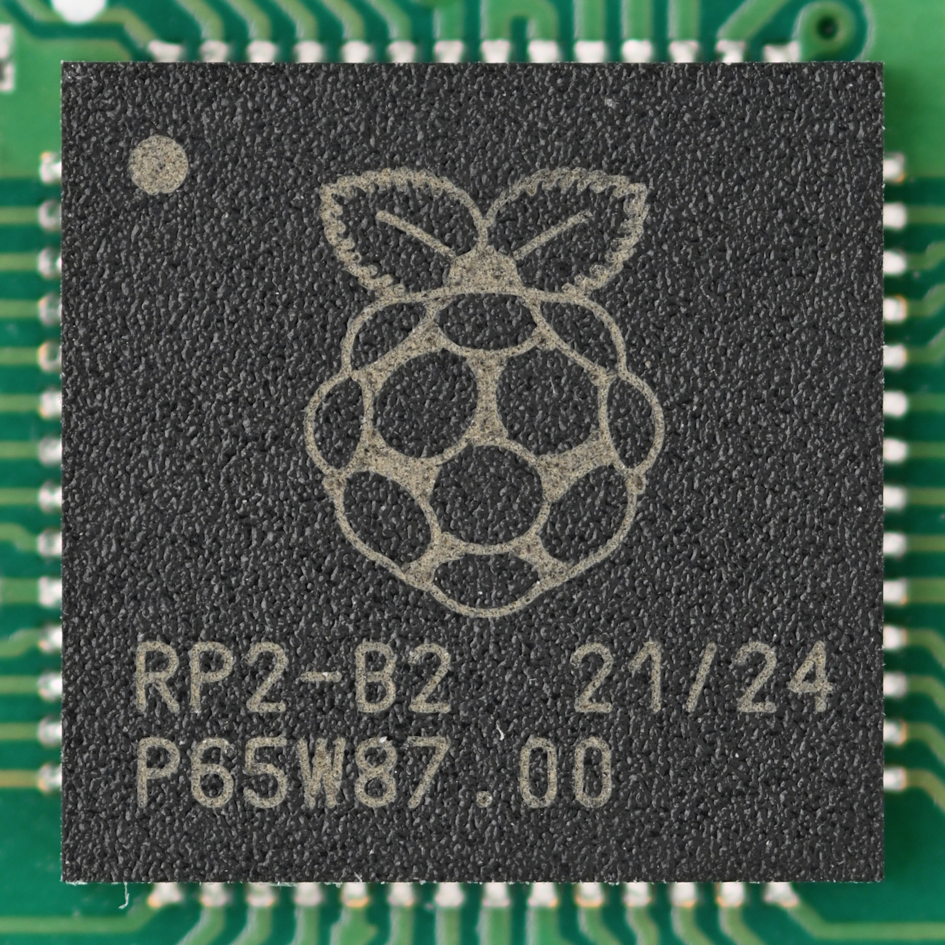
[edit]The RP2040 chip is a 7-by-7-millimetre (0.28 in × 0.28 in) QFN-56EP surface-mount device (SMD) package manufactured by TSMC using its 40 nm process.[16]
- Key features:[17]
- Dual ARM Cortex-M0+ cores (ARMv6-M instruction set), Originally run at 133 MHz,[2] but later certified at 200 MHz[18]
- Each core has an integer divider peripheral and two interpolators
- 264 KB SRAM in six independent banks (four 64 KB, two 4 KB)
- No internal flash or EEPROM memory (after reset, the boot-loader loads firmware from either external flash memory or USB into internal SRAM)
- QSPI bus controller supports up to 16 MB of external flash memory
- DMA controller, 12 channel, 2 IRQ
- AHB crossbar, fully-connected
- On-chip programmable low-dropout regulator (LDO) to generate core voltage
- Two on-chip PLLs to generate USB and core clocks
- 30 GPIO pins, of which four can optionally be used as analog inputs
- Dual ARM Cortex-M0+ cores (ARMv6-M instruction set), Originally run at 133 MHz,[2] but later certified at 200 MHz[18]
- Peripherals:
- One USB 1.1 (LS & FS) controller and PHY, host and device support, 1.5 Mbit/s (Low Speed) and 12 Mbit/s (Full Speed)
- Two UART controllers
- Two SPI controllers
- One QSPI (quad SPI) controller (SSI), supports 1 / 2 / 4-bit SPI transfers, 1 chip select
- Two I²C controllers
- Eight PIO (programmable input–output) state machines
- 16 PWM channels
- 4-channel 12-bit 500-ksps SAR ADC, extra channel is connected to internal temperature sensor
For comparison with the RP2350, see RP2350 § Family comparison.
Boards
[edit]A number of manufacturers have announced their own boards using the RP2040. A selection of the growing number is here:
| Board name | Manufacturer | Size (mm) | Header pins | Debug connection | Number of pads | USB connector | Other connectors | Flash size | GPIO pins | ADC pins | Buttons | Other features | Image |
|---|---|---|---|---|---|---|---|---|---|---|---|---|---|
| Pico[19] | Raspberry Pi Ltd | 51×21 | 40+3 | via headers | 6 | micro-USB | 2 MB | 26 | 3 | BOOTSEL | 
| ||
| Pico W[20] | Raspberry Pi Ltd | 51×21 | 40+3 | via headers | 6 | micro-USB | 2 MB | 26 | 3 | BOOTSEL | Wi-Fi, Bluetooth | .jpg)
| |
| XIAO RP2040[21] | Seeed Studio | 20×17.5×3.5 | 14 | Reset Button/ Boot Button | USB Type-C interface | 2 MB | BOOTSEL + RESET | ||||||
| Nano RP2040 Connect[22] | Arduino | 45×18 | 30 | via pads | 5+4+2 | micro-USB | 16 MB | 1 | Wi-Fi, Bluetooth, 9-axis IMU, microphone | .jpg)
| |||
| Tiny 2040[23] | Pimoroni | 22.9×18.2×6 | 8+3 | via headers | USB-C | 8 MB | 12 | 4 | BOOTSEL + RESET | ||||
| Keybow 2040[24] | Pimoroni | 76x76x30 | 0 (USB only) | USB-C | 2 MB | 16 keys | |||||||
| PicoSystem[25] | Pimoroni | 96.6×42.7×15.5 | 0 (self contained) | USB-C | 16 MB | 4 + joypad | Color 240×240 LCD, onboard battery | ||||||
| Feather RP2040[26] | Adafruit | 51×23×7 | 28 | via pins | USB-C | STEMMA QT, lipo battery | 8 MB | 21 | 4 | BOOTSEL + RESET | Battery charger | ||
| ItsyBitsy RP2040[27] | Adafruit | 36×18×4 | 33 | via headers | micro-USB | 4 MB | 23 | 4 | BOOTSEL + RESET | ||||
| Metro RP2040[28] | Adafruit | 71x53×13 | 32 | SWD + 3 pin JST SH compatible | USB Type-C | DC jack for 6-12VDC / STEMMA QT / SWD / pico probe | 16 MB | 24 | 4 | BOOTSEL + RESET | NeoPixel LED, Micro SD | ||
| QT Py RP2040[29] | Adafruit | 22×18×6 | 14 | Reset Button/ Boot Button | USB-C | STEMMA QT | 8 MB | 13 | 4 | BOOTSEL + RESET | 3.3vdc regulator, NeoPixel LED | ||
| Pro Micro – RP2040[30] | Sparkfun | 36×18 | 24 | 4+2 | USB-C | QWIIC | 16 MB | 20 | 4 | BOOTSEL + RESET | .jpg)
| ||
| Thing Plus RP2040[31] | Sparkfun | 59×23 | 28 | JTAG pins | USB-C | QWIIC, lipo battery | 16 MB | 18 | 4 | BOOTSEL + RESET | Battery charger | .jpg)
| |
| MicroMod RP2040[32] | Sparkfun | 22×22 | 0 | edge connector | edge connector | 16 MB | 29 | 3 | none | .jpg)
| |||
| Müsli USB Pmod[33] | Lone Dynamics | 45×20.32 | 12 | SWD | USB Type-A female | 12-pin male PMOD, SWD | 256 KB | 8 | 0 | BOOTSEL | USB host, 5V boost converter | ||
| Werkzeug USB Multi-Tool[34] | Lone Dynamics | 50×50 | 32 | USB-C | 12-pin female PMOD, USB Type-A female | 1 MB | 24 | 4 | BOOTSEL | USB device/host, PMOD | |||
| RP2040[35] | WeAct Studio | 53x21.52 | 40+4 | via headers | USB-C | 2 MB, 4 MB, 8 MB, 16 MB |
26 | 4 | BOOTSEL + RESET | ||||
| RP2040-Zero[36] | Waveshare Electronics | 23×18 | 23 | USB-C | 10-pad connector | 2 MB | 29 | 4 | BOOTSEL + RESET | RGB LED (WS2812) | |||
| Pico2040 | zeankun.dev | 51x18 | 40+3 (2mm and 2.54mm variants are available) | SWD | 4 | micro-USB | 16 MB, 32 MB, 64 MB, 128 MB |
28 | 4 | BOOTSEL + RESET | |||
| Bus Pirate 5 | Where Labs, LLC | 60x37 | 10+9 | SWD | USB-C | 16MB | |||||||
| W5100S-EVB-Pico[37] | WIZnet Co., Ltd. | 75x21 | 40+3 | via headers | Micro-USB | RJ45 | 2 MB | 26 | 3 | BOOTSEL + RESET | Ethernet | 
| |
| W5500-EVB-Pico[38] | WIZnet Co., Ltd. | 75x21 | 40+3 | via headers | Micro-USB | RJ45 | 2 MB | 26 | 3 | BOOTSEL + RESET | Ethernet | 
| |
| W6100-EVB-Pico[39] | WIZnet Co., Ltd. | 75x21 | 40+3 | via headers | Micro-USB | RJ45 | 2 MB | 26 | 3 | BOOTSEL + RESET | Ethernet | 
| |
| WizFi360-EVB-Pico[40] | WIZnet Co., Ltd. | 75×21 | 40+3 | via headers | Micro-USB | 2 MB | 26 | 3 | BOOTSEL + RESET | Wi-Fi | 
| ||
| 0xCB-Helios[41] | 0xCB | 36×18 | 40+3 | via headers | USB-C | 16 MB | 29 | BOOTSEL + RESET | default off red power LED, blue user LED, level shifter to drive 5V components. ESD protection chip onboard | ||||
| Picopad[42] | Pájeníčko s.r.o. | 129x53 | 12 | via headers | micro-USB | microSD, external connector | 2 MB | 6 | BOOTSEL + RESET | on-off, Wi-Fi, micro SD card, external connector, IPS screen, speaker, battery | |||
| MUREX ANYESC[43] | MUREX Robotics | 78×35 | 3 | via headers | USB-C | edge connector | 8 MB | 3 | 0 | BOOTSEL + RESET | commercial ESC connector, 3 user LEDs | ||
| RP2040-PICO30[44] | OLIMEX Ltd | 51×21 | 40+3 | via headers | USB-C | Optional UEXT (pUEXT) | 2 MB | 30 | 4 | BOOTSEL + RESET | 3.3V 2A (3A peak) DCDC, All 30 GPIOs available to the user, Optional status LED | ||
| RP2040-PICO30-16[44] | OLIMEX Ltd | 51×21 | 40+3 | via headers | USB-C | Optional UEXT (pUEXT) | 16 MB | 30 | 4 | BOOTSEL + RESET | |||
| PicoUSB[45] | VoltMake[46] | 45×12x4 | 0 (USB only) | Dual sided USB-A | 2 MB | BOOTSEL + MODE | status LED | 
|
See also
[edit]- Arduino – a popular microcontroller board family
- ESP32 – a series of low-cost, low-power system on a chip microcontrollers with integrated Wi-Fi and dual-mode Bluetooth.
- STM32 – a family of 32-bit microcontroller integrated circuits
- Raspberry Pi – Raspberry Pi's series of small single board computers
- Thumby (console) – a thumb-sized micro-console powered by the RP2040
References
[edit]- ^ a b c d "Meet Raspberry Silicon: Raspberry Pi Pico now on sale at $4". January 21, 2021.
- ^ a b "RP2040 Datasheet" (PDF). Raspberry Pi Ltd. Retrieved 20 February 2021.
- ^ Adams, James (1 February 2021). "Raspberry Pi RP2040: Our Microcontroller for the Masses". Arm Blueprint. Retrieved 20 February 2021.
- ^ zeptoforth, GitHub, 2025-10-09, retrieved 2025-10-09
- ^ apple/swift-embedded-examples, Apple, 2024-06-14, retrieved 2024-06-14
- ^ "Rust on the RP series of microcontrollers". GitHub. Retrieved 29 March 2023.
- ^ "Raspberry Pi Pico". TinyGo. Retrieved 2024-09-10.
- ^ Rembor, Kattni. "Getting Started with Raspberry Pi Pico and CircuitPython". Adafruit Learning System. Adafruit. Retrieved 17 February 2023.
- ^ "PicoRuby R2P2". Retrieved 19 Nov 2025.
- ^ "Ada on the Raspberry Pi Pico". Retrieved 10 July 2023.
- ^ "RP2040 | DeviceScript". microsoft.github.io. Retrieved 2023-11-28.
- ^ microzig, Zig Embedded Group, 2024-12-08, retrieved 2024-12-08
- ^ "Tweet". twitter.com. Retrieved 2021-02-18.
- ^ Williams, Elliot (20 January 2021). "Raspberry Pi Enters Microcontroller Game With $4 Pico". Hackaday. Retrieved 20 February 2021.
- ^ "RP2040 datasheet" (PDF). Raspberry Pi Ltd. 2 May 2024. p. 391.
There are two hardware issues with the device controller, both of which have software workarounds on RP2040B0, RP2040B1, and are fixed in hardware on RP2040B2
- ^ "Raspberry Pi: Here's how we built our own chip to power the Pico". ZDNET. Retrieved 2023-10-05.
- ^ "RP2040 Datasheet" (PDF). raspberrypi.com. Retrieved 2021-03-28.
- ^ "Pico SDK 2.1.1".
- ^ "Buy a Raspberry Pi Pico".
- ^ "Pico W - Raspberry Pi | Rasppishop - Raspberry Pi Boards und Zubehör". Pico W - Raspberry Pi | Rasppishop - Raspberry Pi Boards und Zubehör (in German). Retrieved 2023-09-04.
- ^ "Seeed Studio XIAO RP2040 - Supports Arduino, MicroPython and CircuitPython". www.seeedstudio.com. 2023-08-06. Retrieved 2023-09-04.
- ^ "Welcome Raspberry Pi to the world of microcontrollers". 20 January 2021.
- ^ "Tiny 2040 – Pimoroni".
- ^ "Keybow 2040 – Pimoroni".
- ^ "PicoSystem – Pimoroni".
- ^ "Adafruit Feather RP2040".
- ^ "Adafruit ItsyBitsy RP2040".
- ^ "Adafruit Metro RP2040".
- ^ "Adafruit QT Py RP2040".
- ^ "SparkFun Pro Micro - RP2040 - DEV-18288 - SparkFun Electronics".
- ^ "SparkFun Thing Plus - RP2040 - DEV-17745 - SparkFun Electronics".
- ^ "SparkFun MicroMod RP2040 Processor - DEV-17720 - SparkFun Electronics".
- ^ "Müsli USB Pmod™ Compatible Module".
- ^ "Werkzeug USB Multi-Tool".
- ^ Studio, WeAct (2023-08-17), RP2040 / WeAct Studio 微行工作室 出品, retrieved 2023-09-04
- ^ "RP2040-Zero, A Low-Cost, High-Performance Pico-Like MCU Board Based On Raspberry Pi Microcontroller RP2040". www.waveshare.com. Retrieved 2023-09-04.
- ^ "WIZnet W5100S-EVB-Pico".
- ^ "WIZnet W5500-EVB-Pico".
- ^ "WIZnet W6100-EVB-Pico".
- ^ "WIZnet WizFi360-EVB-Pico".
- ^ "0xCB Helios". GitHub.
- ^ "Picopad".
- ^ "ESC – MUREX Robotics Documentation". docs.murexrobotics.com. Retrieved 2024-07-07.
- ^ a b "RP2040-PICO30 - Open Source Hardware Board". Olimex. Retrieved 2024-07-19.
- ^ "PicoUSB: Raspberry Pi (Pico) RP2040 powered Bad USB (Rubber Ducky)". PicoUSB. Retrieved 2024-09-29.
- ^ "VoltMake - Electronics Engineering - PCB Design - Firmware - Software". VoltMake. Retrieved 2024-09-29.
External links
[edit]
RP2040
View on GrokipediaDevelopment and Release
Background and Design
The Raspberry Pi Foundation developed the RP2040 microcontroller to address the need for an affordable, high-performance chip tailored for hobbyists, educators, and embedded developers, emphasizing ease of use in GPIO-intensive applications without dependence on third-party silicon vendors. This initiative stemmed from the Foundation's long-standing mission to democratize computing, extending their single-board computer expertise into the microcontroller domain to enable low-cost prototyping and educational projects focused on physical interfacing. By designing the chip in-house, the team aimed to incorporate signature values of high performance, low cost, and accessibility, filling a gap for a versatile device optimized for custom peripherals and real-time control tasks.[1][5] Development of the RP2040 began in the summer of 2017, led by a team of Raspberry Pi engineers who prioritized a dual-core ARM Cortex-M0+ architecture for its balance of simplicity, low power, and cost-effectiveness in implementation. The design process involved extensive use of Verilog for hardware description, with rigorous verification through software simulators and FPGA prototypes to ensure reliability before tape-out. Key phases included synthesizing the design for target performance, integrating design-for-test (DFT) features, and iterating on layout to meet area and power constraints, culminating in initial silicon validation on bring-up boards with separate power supplies to monitor and limit current draw during testing.[5][6] The RP2040 was fabricated using TSMC's 40LP (40 nm low-power) process node, selected for its optimal trade-off between performance, dynamic power efficiency, and leakage control, enabling operation at a nominal system clock speed of 125 MHz (up to 133 MHz maximum). Power consumption targets emphasized sub-100 mW active operation, achieved through efficient clocking options, low-power modes, and on-chip regulation, with typical figures around 0.4–0.6 mW per MHz under load. To facilitate prototyping, the RP2040 provides 30 GPIO pins, allowing for board designs with 0.1-inch pin spacing compatibility for standard breadboard setups, as seen in the reference Raspberry Pi Pico board, alongside open-source hardware elements such as KiCad reference schematics and layout guidelines to encourage community-driven board designs.[1][5][7]Announcement and Production
The RP2040 microcontroller was publicly unveiled by the Raspberry Pi Foundation on January 21, 2021, in conjunction with the launch of the Raspberry Pi Pico development board, marking Raspberry Pi's entry into in-house silicon design for microcontrollers.[3] The chip was positioned as an affordable option for embedded applications, with the Pico board priced at $4, while the standalone RP2040 became available for purchase at $1 per unit starting June 1, 2021, through approved resellers.[3][4] Production of the RP2040 began ramping up in early 2021 at TSMC's facilities using a 40 nm process, but faced significant delays due to the global semiconductor shortages that intensified that year, resulting in widespread backorders for the Pico board and related products.[8] Despite these challenges, Raspberry Pi produced over 10 million RP2040 chips in 2021 alone, demonstrating robust scaling once supply stabilized. By 2025, annual production continues at scale, with projections of around 10 million units shipped that year.[8][9] The chip is offered in a QFN-56 package for standard integration or as a bare die for custom multi-chip modules, with its full datasheet released under a Creative Commons Attribution-NoDerivatives 4.0 International license to facilitate broad adoption.[1][10] Subsequent silicon revisions, including steppings B1 and B2 following the initial B0, introduced fixes to the boot ROM and other minor enhancements to improve reliability and manufacturing yields, with B2 becoming the standard by mid-2021.[1] As of 2025, the RP2040 remains in active production with a guaranteed lifespan until at least January 2041, widely available through major distributors such as Digi-Key and Mouser Electronics in both single-unit and bulk quantities.[1][11][12][13]Architecture
Processor Cores
The RP2040 microcontroller integrates two ARM Cortex-M0+ processor cores, designed for low-power embedded applications with a focus on efficiency and simplicity. Each core implements the ARMv6-M architecture, supporting a 32-bit Thumb and Thumb-2 instruction set for compact code density and deterministic execution. Operating at a nominal clock frequency of 133 MHz, the cores can be officially overclocked to 200 MHz when supplied with a core voltage of at least 1.15 V, enabling higher performance in demanding tasks while maintaining compatibility with the device's thermal and power constraints.[1][14] The Cortex-M0+ cores lack a hardware floating-point unit (FPU), relying instead on software-based floating-point operations provided by a fast library in the RP2040's boot ROM to handle single-precision arithmetic efficiently. This design choice prioritizes die area and power savings over native floating-point hardware, aligning with the microcontroller's cost-sensitive profile. Each core delivers approximately 0.95 DMIPS/MHz in performance, offering balanced integer processing suitable for real-time control and signal processing without the overhead of more complex architectures.[1][15] Inter-core communication is facilitated through the Single-cycle I/O (SIO) block, which includes two 32-bit, 8-entry FIFO buffers—one for each direction—allowing efficient data transfer between cores at up to four words per cycle. Synchronization is managed via 32 hardware mutexes (spinlocks), enabling lock-free parallel task execution across the cores without requiring a memory management unit (MMU), which is absent in the Cortex-M0+ design. This setup supports asymmetric multiprocessing, where one core can handle system tasks while the other runs application code, promoting scalability in multi-threaded firmware.[1][14] Power management for the cores is optimized through separate voltage domains: the digital core operates at a nominal 1.1 V (DVDD, range 1.05–1.16 V), while I/O interfaces use 3.3 V (IOVDD, range 1.8–3.6 V). Dynamic clock gating at the core level, controlled via registers like SLEEP_EN and WAKE_EN, allows individual cores to be powered down or slowed independently, reducing energy consumption during idle periods or when only one core is active. This granular control, combined with the PLL-based clock system, ensures the RP2040 achieves low quiescent current, making it ideal for battery-powered devices.[1][7] The cores can offload repetitive I/O operations to the Programmable I/O (PIO) subsystem for enhanced parallelism, though without dedicated vector extensions or SIMD instructions on the processors themselves.[1]Memory System
The RP2040 microcontroller features 264 kB of on-chip static random-access memory (SRAM), organized into six independent banks comprising four 64 kB banks and two 4 kB banks.[1] This architecture enables high-bandwidth access by allowing parallel reads and writes across banks, with the SRAM logically appearing as a contiguous block but physically striped for improved performance in multi-master scenarios.[1] The memory can be configured flexibly, such as as a single 264 kB block for unified use or split into two 128 kB regions (one per core) plus an 8 kB shared region, often achieved through the Memory Protection Unit (MPU) or by direct bank allocation to support dual-core operation without contention.[1] The RP2040 lacks a dedicated external memory controller for general-purpose DRAM; however, it includes hardware support for execute-in-place (XIP) access to up to 16 MB of off-chip QSPI flash memory via a dedicated interface, with additional flexibility provided by the Programmable I/O (PIO) subsystem for custom flash protocols if needed.[1] The RP2040 employs a 32-bit address space spanning 4 GB (from 0x00000000 to 0xFFFFFFFF), facilitating straightforward memory mapping for its components.[1] The shared SRAM is mapped to 0x20000000–0x20041FFF, accessible by both processor cores, DMA controllers, and peripherals over the AHB-Lite bus fabric.[1] An 16 kB boot ROM, containing the initial bootloader and utility functions, resides at 0x00000000–0x00003FFF and executes automatically on reset to handle system initialization.[1] External QSPI flash for code storage is mapped to 0x10000000–0x10FFFFFF, enabling direct execution without mandatory copying to SRAM, though the boot sequence typically loads initial code into RAM for faster operation.[1] Other regions include peripheral registers at 0x40000000 (APB) and 0x50000000 (AHB-Lite), ensuring isolation from system memory.[1] Error handling in the memory system relies primarily on software mechanisms, as the hardware does not include built-in parity or error correction code (ECC) for SRAM; developers can implement optional ECC in software for critical applications.[1] The boot process begins in the ROM, which checks the external flash via the QSPI interface: it loads the first 256 bytes of flash into SRAM bank 5, verifies integrity using CRC32, and jumps to execution if valid, otherwise falling back to USB bootloader mode after a timeout.[1] This sequence ensures reliable code loading into RAM, supporting stateless operation where the device boots from external flash without internal non-volatile storage.[1] The SRAM supports dual-port access, permitting simultaneous reads by both cores or other masters without arbitration delays in most cases, thanks to the banked structure and dedicated AHB-Lite paths.[1] Operating at the system clock speed of up to 133 MHz, it provides zero-wait-state, single-cycle 32-bit access, yielding effective bandwidths of up to 133 MB/s per port or higher aggregate throughput (e.g., 2 GB/s peak for interleaved accesses).[1] This design prioritizes low-latency data movement for real-time tasks, with core access patterns leveraging the shared mapping to enable efficient inter-core communication via SRAM.[1]Key Features
Programmable I/O (PIO)
The RP2040 microcontroller incorporates a dedicated Programmable I/O (PIO) subsystem consisting of two independent PIO blocks, each equipped with four state machines, for a total of eight state machines that enable parallel execution of custom assembler programs tailored to bit-banging protocols and other specialized digital interfaces.[1] This architecture allows the state machines to operate autonomously, offloading the dual-core Arm Cortex-M0+ processors from timing-critical I/O tasks while providing deterministic behavior essential for protocols requiring precise pulse widths or synchronization.[1] Each PIO block shares a 32 × 16-bit instruction memory space, permitting flexible program allocation across its state machines, which can run concurrently to handle multiple independent I/O streams.[1] The PIO instruction set comprises compact 16-bit instructions designed for efficient I/O manipulation, including primitives such as IN and OUT for shifting data to and from GPIO pins, JMP for conditional or unconditional branching to implement loops and control flow, and WRAP directives in the execution control registers to define program boundaries for seamless cycling without CPU intervention.[1] Additional instructions like MOV, SET, WAIT, PUSH, PULL, DELAY, and IRQ support data movement, pin setting, synchronization on GPIO or IRQ conditions, FIFO transfers, timing adjustments, and interrupt generation, enabling the creation of complex behaviors within a minimal footprint of up to 32 instructions per block.[1] Each state machine executes these instructions in a single cycle relative to its clock domain, with clock speeds derived from the system clock (up to 133 MHz by default) via programmable 16.8 fixed-point dividers, allowing independent operation at frequencies from approximately 2 kHz to the full system rate for high-throughput applications.[1] Buffering is handled through 4 × 32-bit TX and RX FIFOs per state machine, which can be joined into 8 × 32-bit single-direction FIFOs using shift control configuration, facilitating efficient data staging between the PIO and the rest of the system with minimal latency.[1] Autopull and autopush mechanisms, configurable with bit-width thresholds from 1 to 32, automate transfers between FIFOs and the 32-bit input/output shift registers, while DMA request (DREQ) signals enable chaining with the RP2040's DMA controller for sustained, low-CPU-overhead data transfers across peripherals.[1] This integration supports burst transfers at up to one word per clock cycle, as detailed in the microcontroller's peripheral documentation.[1] PIO's flexibility shines in practical implementations, such as driving WS2812 addressable LEDs, where a compact program (often 3-4 instructions) generates the required 800 kHz serial protocol with precise 400 ns and 800 ns high-time pulses per bit, using a single state machine to control an arbitrary number of LEDs in a chain via DMA-fed FIFO data. Similarly, VGA output can be achieved by configuring state machines for parallel digital pixel interface (DPI) signaling, outputting 16-bit RGB-565 video data across 18 GPIOs with resistor-based DAC conversion for analog sync and color levels, demonstrating PIO's capability for video timing without dedicated hardware.[7] State machines support on-the-fly reconfiguration through core-initiated commands to execution control registers, allowing dynamic shifts in pin mappings, program loading, or operational modes—such as pausing one machine to repurpose GPIOs for a different protocol—while maintaining overall system responsiveness.[1] PIO is also commonly used to implement I²S audio output for interfacing with external DACs, such as the PCM510xA series, in a 3-wire configuration (BCLK, LRCK, DATA) without requiring an external master clock since many DACs have internal PLLs that lock from BCK. A popular efficient approach uses a single PIO state machine with .side_set 2 to control both BCLK (side-set bit 0) and LRCK (side-set bit 1) alongside the DATA pin via out pins. The program shifts out bits MSB-first, using the X register as a bit counter in loops for each channel. Example PIO assembly for 32-bit per channel (64-bit stereo frame):.side_set 2
bitloop_left:
out pins, 1 side 0b10 ; BCLK high, LRCK low (left channel)
jmp x-- bitloop_left side 0b11
out pins, 1 side 0b00
set x, 30 side 0b01
bitloop_right:
out pins, 1 side 0b00 ; BCLK low, LRCK low (transition)
jmp x-- bitloop_right side 0b01
out pins, 1 side 0b10
set x, 30 side 0b11 ; LRCK high for right channel
set x, 30 to set x, 14. The program assumes autopull with pull_threshold(32), shifting left (MSB-first), and TX FIFO fed with one 32-bit word per channel.
Clock configuration is critical for standard audio rates. For example, to achieve 96 kHz sample rate with 64× BCK (6.144 MHz BCLK), set the PIO clock divider to 10 when the system clock is configured to 61.44 MHz (61.44 MHz / 10 = 6.144 MHz). Many DACs like PCM510xA support 32× or 64× BCK per LRCK; refer to the datasheet for PLL locking ranges (e.g., 3.072 MHz or 6.144 MHz at 96 kHz).
This PIO method offloads audio generation entirely to hardware, allowing sustained high-quality playback with DMA feeding the FIFO from memory buffers, making it ideal for embedded audio applications on the RP2040.
Integrated Peripherals
The RP2040 microcontroller integrates a variety of fixed-function peripherals designed for efficient handling of communication, analog input, timing, and data transfer tasks, all accessible via the ARM bus and configurable through dedicated registers. These peripherals operate from the peripheral clock domain (clk_peri, up to 133 MHz) and support direct memory access (DMA) for offloading CPU involvement in data movement. Electrical characteristics include support for IOVDD supplies from 1.8 V to 3.3 V, with GPIO drive strengths configurable up to 12 mA.[1]Communication Interfaces
The RP2040 features two UART controllers (UART0 and UART1), each supporting 5- to 8-bit data words, 1 or 2 stop bits, optional parity (odd, even, or none), and hardware flow control via RTS/CTS signals. They include 32-entry transmit FIFOs and 32-entry receive FIFOs, with programmable baud rates derived from the peripheral clock (clk_peri) up to approximately 7.8 Mbaud at 125 MHz system clock. Interrupt sources include receive/transmit FIFO level thresholds and overrun conditions, mapped to IRQ 20 (UART0) and IRQ 21 (UART1).[1] Two SPI controllers (SPI0 and SPI1) provide master and slave modes compatible with Motorola SPI, Texas Instruments SSP, and Microwire formats, including dual/quad data modes for up to 32-bit frames. Each has 8-deep transmit and receive FIFOs, with clock rates up to 62.5 Mbps in master mode or 11 Mbps in slave mode at 133 MHz clk_peri. Configuration options include programmable clock polarity/phase and data size, with interrupts for FIFO events on IRQ 18 (SPI0) and IRQ 19 (SPI1). DMA channels can be paced by dedicated request signals for efficient burst transfers.[1] Additionally, two I2C buses (I2C0 and I2C1) support standard (100 kHz), fast (400 kHz), and fast-plus (1 MHz) modes in both master and slave configurations, using 7- or 10-bit addressing. Each includes 16-deep transmit/receive FIFOs, clock stretching for slave synchronization, and spike suppression filters, with external pull-up resistors required on SDA/SCL lines. Interrupts cover FIFO thresholds and arbitration loss, assigned to IRQ 23 (I2C0) and IRQ 24 (I2C1), and baud rates are programmable up to the system clock limit of 133 MHz.[1]Analog and Timing
The analog subsystem centers on a single 12-bit successive approximation register (SAR) ADC with four external channels multiplexed to GPIO26–29, plus an internal temperature sensor channel, achieving up to 500 ksps conversion speed from a dedicated 48 MHz CLK_ADC. It delivers 8.7 effective number of bits (ENOB) with differential nonlinearity (DNL) peaks at specific codes, optimized for input voltages up to 3.3 V under ADC_AVDD of 1.8–3.3 V; an 8-entry FIFO buffers results, with DMA support via IRQ 22.[1] For pulse-width modulation, the RP2040 provides eight PWM slices, each generating two independent 16-bit channels (A and B) for a total of 16 outputs, supporting arbitrary duty cycles from 0–100% with phase-correct operation and fractional clock division (up to 8.4 fixed-point precision). Counters derive from clk_peri, enabling high-resolution control for motor drives or LED dimming, with DMA pacing and a shared interrupt (IRQ 4).[1] Timing functions include a 64-bit system timer with four independent alarm comparators, clocked by the reference clock (clk_ref, 12 MHz default) for resolutions down to 1 µs and maximum intervals up to approximately 4295 seconds, generating interrupts on IRQ 0–3. A dedicated 24-bit watchdog timer, extendable to 64-bit via software, provides system reset on underflow and non-maskable interrupt (NMI) support, with a maximum timeout of about 8.3 seconds at 1 µs ticks; it includes scratch registers for state preservation.[1]USB Controller
The integrated USB 1.1 controller operates at full speed (12 Mbps) with an on-chip PHY, supporting device mode natively and host mode through software implementation. It manages up to 32 endpoints (8 addressable) with 60 × 64-byte buffers in 4 kB of dedicated DPRAM, handling control, bulk, interrupt, and isochronous transfers; low-speed (1.5 Mbps) host operation is possible via an external hub. The 48 MHz USB clock (CLK_USB) requires clk_sys > 48 MHz, with interrupts on IRQ 5 for endpoint events; electrical specs include 27 Ω series resistors on D+/D- lines and VBUS sensing via GPIO. Double buffering enhances throughput, though certain endpoint abort operations require software workarounds.[1]DMA
The direct memory access controller comprises 12 independent channels, each capable of 8-, 16-, or 32-bit transfers with scatter-gather support via chaining and programmable priority levels. It facilitates burst transfers to/from peripherals like UART, SPI, I2C, ADC, and PWM using dedicated data request (DREQ) signals, with pacing timers and optional CRC computation for integrity. Sequences can handle up to 2^32 - 1 transfers, generating interrupts on completion (IRQ 11 for channels 0–5, IRQ 12 for 6–11); address incrementing and wrapping modes are configurable, though certain read/write address behaviors during non-incrementing transfers necessitate using transfer count registers instead.[1]Package
The RP2040 microcontroller is housed in a QFN-56 (Quad Flat No-leads) package with a body size of 7 mm × 7 mm and a pin pitch of 0.4 mm. The central exposed GND pad (ePad) measures 3.2 mm × 3.2 mm and is reduced in size compared to standard QFN-56 packages to facilitate easier PCB routing between the pad and the peripheral pins.[1] Recommended PCB footprint dimensions include an overall size of 7.75 mm × 7.75 mm, with pad width 0.20 mm, inner pad length 0.875 mm, and outer pad length 1.175 mm.[1] The RP2040 is Pb-free with matte tin finish (minimum 8 µm over CuFe2P). It has Moisture Sensitivity Level 1 (MSL1) per J-STD-020E. The recommended reflow profile includes: preheat 150–200°C for 60–120 s, peak temperature 260°C for 30 s, ramp-up ≤3°C/s, time above 217°C 60–150 s, ramp-down ≤6°C/s, total time ≤8 min. Adjust for actual board assembly.[7]Programming and Development
Software Development Kit (SDK)
The Raspberry Pi Pico SDK, also known as pico-sdk, is the official open-source software development kit for programming the RP2040 microcontroller in C and C++. Released on January 21, 2021, alongside the Raspberry Pi Pico board, it provides a comprehensive framework for embedded development, emphasizing simplicity and direct hardware access while abstracting low-level details. The SDK is actively maintained, with version 2.2.0 released in July 2025, including bug fixes, documentation improvements, and new features such as enhanced board support.[16][17] The SDK is built on ARM's Cortex Microcontroller Software Interface Standard (CMSIS) for core functionality and supports optional integration with FreeRTOS for real-time operating system capabilities. It includes hardware abstraction layers with APIs for key RP2040 features, such as general-purpose input/output (GPIO) control viagpio_init() and related functions, Programmable I/O (PIO) state machines for custom protocols, and peripherals like timers, UART, SPI, I2C, PWM, and ADC. These APIs enable developers to configure and interact with hardware registers without manual bit manipulation in most cases, promoting portable and maintainable code.[18][17][16]
The build system is CMake-based (version 3.13 or later), facilitating cross-compilation for the ARM Cortex-M0+ architecture using the GNU ARM Embedded Toolchain (GCC). Developers clone the SDK repository, set the PICO_SDK_PATH environment variable, and generate build files with commands like cmake -B build followed by make in the build directory; board-specific configurations, such as for the Pico or Pico W, are specified via -DPICO_BOARD flags. The SDK incorporates a bootloader called boot2, which supports USB mass storage (UF2 files) and UART-based flashing for drag-and-drop or scripted deployment without additional hardware.[18][17][16]
Debugging is facilitated through the RP2040's Serial Wire Debug (SWD) interface, compatible with tools like the official Raspberry Pi Debug Probe or a secondary Pico configured as a Pico Probe via USB. The SDK supports GDB integration for breakpoints and stepping, along with printf redirection over USB serial output and hardware trace capabilities using the ARM CoreSight components for performance analysis.[19][18][17]
The SDK ships with a repository of pre-built examples in the companion pico-examples project, demonstrating core concepts such as a basic LED blinker using GPIO, PIO-based animations like VGA signal generation, and USB device classes including Human Interface Device (HID) for keyboard or mouse emulation. These examples serve as starting points for custom applications and highlight the SDK's versatility for both simple bare-metal programs and more complex multicore designs.[20][18]
Supported Languages and Ecosystems
The RP2040 microcontroller supports a variety of programming languages and ecosystems beyond its primary C/C++ SDK, enabling rapid prototyping and accessibility for developers from diverse backgrounds. These include interpreted languages like Python variants, as well as support for Rust, Go, and JavaScript through community-driven ports and libraries. Such ecosystems emphasize ease of use, interactive development, and integration with popular tools, fostering widespread adoption in education, hobbyist projects, and embedded applications.[21][22][23] MicroPython provides an official port for the RP2040, offering a lightweight Python 3 implementation optimized for microcontrollers. It includes a REPL (Read-Eval-Print Loop) accessible over USB for immediate interactive coding, along with themachine.Pin module for GPIO control and the rp2 module for accessing RP2040-specific features like Programmable I/O (PIO) state machines. This setup supports rapid prototyping by allowing developers to script hardware interactions without compilation, such as LED blinking or sensor reading, directly on the device. The firmware is built daily and available for download, with extensive documentation covering RP2040 peripherals.[21][24][25]
CircuitPython, developed by Adafruit as a user-friendly fork of MicroPython, extends support to RP2040 boards with enhanced file system access. Users can edit code files directly on the device, which appears as a USB mass storage drive (CIRCUITPY) upon connection, simplifying deployment without specialized tools. It includes a rich library ecosystem for common peripherals, such as sensors (e.g., via adafruit_dht for temperature/humidity) and displays (e.g., adafruit_ssd1306 for OLED screens), promoting circuit-building and experimentation. Official UF2 firmware images are provided for various RP2040-based boards like the Raspberry Pi Pico and Adafruit Feather RP2040.[26][27][28]
For the Seeed Studio XIAO RP2040 board, CircuitPython installation involves downloading the latest UF2 firmware file from the official CircuitPython downloads page. Users hold the BOOT button while connecting the board to a USB port, causing it to appear as the "RPI-RP2" mass storage drive. Dragging the UF2 file onto this drive initiates the installation, after which the board reboots and mounts as the "CIRCUITPY" drive for direct file editing and code execution.[29][30]
Additional languages broaden the RP2040's appeal through community efforts. Rust integration is facilitated by the rp-hal crate, an embedded-HAL implementation providing safe, high-level abstractions for peripherals like timers, UART, and PIO, enabling memory-safe embedded development. TinyGo, a Go compiler for microcontrollers, supports RP2040 with multi-core execution and PIO access as of September 2025, including enhancements for concurrency in tasks like networking on the Pico W. For JavaScript, the Kaluma runtime (version 1.2 as of February 2025) offers a tiny engine tailored for RP2040, supporting Node.js-like APIs for event-driven scripting and hardware control. Arduino IDE compatibility is achieved via community cores, such as the Earle Philhower RP2040 core, which ports the Arduino framework to enable sketch-based programming with familiar libraries like Servo and Wire.[22][31][23][32][33]
These languages integrate with broader ecosystems for streamlined workflows. PlatformIO provides comprehensive RP2040 support, including board definitions, library management, and build tools compatible with MicroPython, CircuitPython, and Arduino frameworks, allowing project configuration via a unified IDE. Visual Studio Code extensions, such as the official Raspberry Pi Pico VS Code extension, offer debugging, flashing, and serial monitoring tailored for RP2040 development across languages. The SDK underpins these runtimes by exposing low-level hardware access.[34][35][36][37]