
Community hub
Recent from talks
Contribute something
Nothing was collected or created yet.
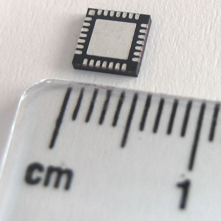
Flat no-leads package
View on Wikipedia
Flat no-leads packages such as quad-flat no-leads (QFN)[1] and dual-flat no-leads (DFN) physically and electrically connect integrated circuits to printed circuit boards. Flat no-leads, also known as micro leadframe (MLF) and SON (small-outline no leads), is a surface-mount technology, one of several package technologies that connect ICs to the surfaces of PCBs without through-holes. Flat no-lead is a near chip scale plastic encapsulated package made with a planar copper lead frame substrate. Perimeter lands on the package bottom provide electrical connections to the PCB.[1] Flat no-lead packages usually, but not always, include an exposed thermally conductive pad to improve heat transfer out of the IC (into the PCB). Heat transfer can be further facilitated by metal vias in the thermal pad.[2] The QFN package is similar to the quad-flat package (QFP), and a ball grid array (BGA).
Flat no-lead cross-section
[edit]
The figure shows the cross section of a flat no-lead package with a lead frame and wire bonding. There are two types of body designs, punch singulation and saw singulation.[3] Saw singulation cuts a large set of packages in parts. In punch singulation, a single package is moulded into shape. The cross section shows a saw-singulated body with an attached thermal head pad. The lead frame is made of copper alloy and a thermally conductive adhesive is used for attaching the silicon die to the thermal pad. The silicon die is electrically connected to the lead frame by 1–2 thou diameter gold wires.
The pads of a saw-singulated package can either be completely under the package, or they can fold around the edge of the package.
Different types
[edit]Two types of QFN packages are common: air-cavity QFNs, with an air cavity designed into the package, and plastic-moulded QFNs with air in the package minimized.
Less-expensive plastic-moulded QFNs are usually limited to applications up to ~2–3 GHz. It is usually composed of just 2 parts, a plastic compound and copper lead frame, and does not come with a lid.
In contrast, the air-cavity QFN is usually made up of three parts; a copper leadframe, plastic-moulded body (open, and not sealed), and either a ceramic or plastic lid. It is usually more expensive due to its construction, and can be used for microwave applications up to 20–25 GHz.
QFN packages can have a single row of contacts or a double row of contacts.
Advantages
[edit]This package offers a variety of benefits including reduced lead inductance, a small sized "near chip scale" footprint, thin profile and low weight. It also uses perimeter I/O pads to ease PCB trace routing, and the exposed copper die-pad technology offers good thermal and electrical performance. These features make the QFN an ideal choice for many new applications where size, weight, thermal and electrical performance are important.
Design, manufacturing, and reliability challenges
[edit]Improved packaging technologies and component miniaturization can often lead to new or unexpected design, manufacturing, and reliability issues. This has been the case with QFN packages, especially when it comes to adoption by new non-consumer electronic OEMs.
Design and manufacturing
[edit]Some key QFN design considerations are pad and stencil design. When it comes to bond pad design two approaches can be taken: solder mask defined (SMD) or non-solder mask defined (NSMD). A NSMD approach typically leads to more reliable joints, since the solder is able to bond to both the top and sides of the copper pad.[4] The copper etching process also generally has tighter control than the solder masking process, resulting in more consistent joints.[5] This does have the potential to affect the thermal and electrical performance of the joints, so it can be helpful to consult the package manufacturer for optimal performance parameters. SMD pads can be used to reduce the chances of solder bridging, however this may affect overall reliability of the joints. Stencil design is another key parameter in QFN design process. Proper aperture design and stencil thickness can help produce more consistent joints (i.e. minimal voiding, outgassing, and floating parts) with proper thickness, leading to improved reliability.[6]
There are also issues on the manufacturing side. For larger QFN components, moisture absorption during solder reflow can be a concern. If there is a large amount of moisture absorption into the package then heating during reflow can lead to excessive component warpage. This often results in the corners of the component lifting off the printed circuit board, causing improper joint formation. To reduce the risk of warpage issues during reflow a moisture sensitivity level of 3 or higher is recommended.[7] Several other issues with QFN manufacturing include: part floating due to excessive solder paste under the center thermal pad, large solder voiding, poor reworkable characteristics, and optimization of the solder reflow profile.[8]
Reliability
[edit]Component packaging is often driven by the consumer electronics market with less consideration given to higher reliability industries such as automotive and aviation. It can therefore be challenging to integrate component package families, such as the QFN, into high reliability environments. QFN components are known to be susceptible to solder fatigue issues, especially thermomechanical fatigue due to thermal cycling. The significantly lower standoff in QFN packages can lead to higher thermomechanical strains due to coefficient of thermal expansion (CTE) mismatch as compared to leaded packages. For example, under accelerated thermal cycling conditions between -40 °C to 125 °C, various quad flat package (QFP) components can last over 10,000 thermal cycles whereas QFN components tend to fail at around 1,000-3,000 cycles.[7]
Historically, reliability testing has been mainly driven by JEDEC,[9][10][11][12] however this has primarily focused on die and 1st level interconnects. IPC-9071A[13] attempted to address this by focusing on 2nd level interconnects (i.e. package to PCB substrate). The challenge with this standard is that it has been more adopted by OEMs than component manufacturers, who tend to view it as an application-specific issue. As a result there has been much experimental testing and finite element analysis across various QFN package variants to characterize their reliability and solder fatigue behavior.[14][15][16][17][18][19][20]
Serebreni et al.[21] proposed a semi-analytical model to assess the reliability QFN solder joints under thermal cycling. This model generates effective mechanical properties for the QFN package, and calculates the shear stress and strain using a model proposed by Chen and Nelson.[22] The dissipated strain energy density is then determined from these values and used to predict characteristic cycles to failure using a 2-parameter Weibull curve.
Comparison to other packages
[edit]The QFN package is similar to the quad flat package, but the leads do not extend out from the package sides. It is hence difficult to hand-solder a QFN package, inspect solder joint quality, or probe lead(s).
Variants
[edit]Different manufacturers use different names for this package: ML (micro-leadframe) versus FN (flat no-lead), in addition there are versions with pads on all four sides (quad) and pads on just two sides (dual), thickness varying between 0.9–1.0 mm for normal packages and 0.4 mm for extremely thin. Abbreviations include:
| Package | Description | Manufacturer |
|---|---|---|
| DFN | dual flat no-lead package | Atmel, ROHM Semiconductor |
| DG1677-2 | quad flat no-lead package | Mini-Circuits |
| DQFN | dual quad flat no-lead package | Atmel |
| cDFN | iC-Haus | |
| TDFN | thin dual flat no-lead package | |
| UTDFN | ultra-thin dual flat no-lead package | |
| XDFN | extremely thin dual flat no-lead package | |
| QFN | quad flat no-lead package | Amkor Technology |
| QFN-TEP | quad flat no-lead package with top-exposed pad | |
| TQFN | thin quad flat no-lead package | |
| LLP | leadless leadframe package | National Semiconductor |
| LPCC | leadless plastic chip carrier | ASAT Holdings |
| MLF | micro-leadframe | Amkor Technology and Atmel |
| MLPD | micro-leadframe package dual | |
| MLPM | micro-leadframe package micro | |
| MLPQ | micro-leadframe package quad | |
| DRMLF | dual-row micro-leadframe package | Amkor Technology |
| DRQFN | dual-row quad flat no-lead | Microchip Technology |
| VQFN/WQFN | very thin quad flat no-lead | Texas Instruments and others (such as Atmel, ROHM Semiconductor) |
| HVQFN | Heatsink Very-thin Quad Flat package | |
| UDFN | ultra dual flat no-lead | Microchip Technology |
| UQFN | ultrathin quad flat no-lead | Texas Instruments and Microchip Technology |

Micro lead frame package (MLP) is a family of integrated circuit QFN packages, used in surface mounted electronic circuits designs. It is available in 3 versions which are MLPQ (Q stands for quad), MLPM (M stands for micro), and MLPD (D stands for dual). These package generally have an exposed die attach pad to improve thermal performance. This package is similar to chip scale packages (CSP) in construction. MLPD are designed to provide a footprint-compatible replacement for small-outline integrated circuit (SOIC) packages.
Micro lead frame (MLF) is a near CSP plastic encapsulated package with a copper leadframe substrate. This package uses perimeter lands on the bottom of the package to provide electrical contact to the printed circuit board. The die attach paddle is exposed on the bottom of the package surface to provide an efficient heat path when soldered directly to the circuit board. This also enables stable ground by use of down bonds or by electrical connection through a conductive die attach material.
A more recent design variation which allows for higher density connections is the dual row micro lead frame (DRMLF) package. This is an MLF package with two rows of lands for devices requiring up to 164 I/O. Typical applications include hard disk drives, USB controllers, and wireless LAN.
See also
[edit]- Chip carrier Chip packaging and package types list
- Quad flat package
References
[edit]- ^ Design requirements for outlines of solid state and related products, JEDEC PUBLICATION 95, DESIGN GUIDE 4.23
- ^ Bonnie C. Baker, Smaller Packages = Bigger Thermal Challenges, Microchip Technology Inc.
- ^ "Archived copy" (PDF). Archived from the original (PDF) on 2006-08-28. Retrieved 2008-09-26.
{{cite web}}: CS1 maint: archived copy as title (link) - ^ http://www.dfrsolutions.com/hubfs/Resources/services/Manufacturing-and-Reliability-Challenges-With-QFN.pdf?t=1503583170559 [bare URL PDF]
- ^ https://www.microsemi.com/document-portal/doc_view/130006-qfn-an [bare URL PDF]
- ^ http://www.dfrsolutions.com/hubfs/Resources/services/Understanding-Criticality-of-Stencil-Aperture-Design-and-Implementation-QFN-Package.pdf [bare URL PDF]
- ^ a b http://www.dfrsolutions.com/hubfs/Resources/services/The-Reliability-Challenges-of-QFN-Packaging.pdf?t=1502980151115 [bare URL PDF]
- ^ http://www.aimsolder.com/sites/default/files/overcoming_the_challenges_of_the_qfn_package_rev_2013.pdf, Seelig, K., and Pigeon, K. "Overcoming the Challenges of the QFN Package," Proceedings of SMTAI, October, 2011.
- ^ JEDEC JESD22-A104D, May 2005, Temperature Cycling
- ^ JEDEC JESD22-A105C, January 2011, Power and Temperature Cycling
- ^ JEDEC JESD22-A106B, June 2004, Thermal Shock
- ^ JEDEC JESD22B113, March 2006, Board Level Cycling Bend Test Method for Interconnect Reliability Characterization of Components for Handheld Electronic Products
- ^ IPC IPC-9701A, February 2006, Performance Test Methods and Qualification Requirements for Surface Mount Solder Attachments
- ^ Syed, A. and Kang, W. "Board level assembly and reliability considerations for QFN type packages." SMTA International Conference, 2003
- ^ Yan Tee, T., et al. "Comprehensive board-level solder joint reliability modeling and testing of QFN and PowerQFN packages." Microelectronics Reliability 43 (2003): 1329–1338.
- ^ Vianco, P. and Neilsen, M. K. "Thermal mechanical fatigue of a 56 I/O plastic quad-flat nolead (PQFN) package." SMTA International Conference, 2015.
- ^ Wilde, J., and Zukowski, E. "Comparative Analysis for μBGA and QFN Reliability." 8th. Int. Conf. on Thermal, Mechanical and Multiphysics Simulation and Experiments in Micro-Electronics and Micro-Systems, 2007 IEEE, 2007.
- ^ De Vries, J., et al. "Solder-joint reliability of HVQFN-packages subjected to thermal cycling." Microelectronics Reliability 49 (2009): 331-339.
- ^ 17. Li, L. et al. "Board level reliability and assembly process of advanced QFN packages." SMTA International Conference, 2012.
- ^ Birzer, C., et al. "Reliability Investigations of Leadless QFN Packages until End-of-Life with Application-Specific Board-Level Stress Tests." Electronics Components and Technology Conference, 2006.
- ^ Serebreni, M., Blattau, N., Sharon, G., Hillman, C., Mccluskey, P. "Semi-analytical fatigue life model for reliability assessment of solder joints in qfn packages under thermal cycling". SMTA ICSR, 2017. Toronto, ON.
- ^ Chen, W. T., and C. W. Nelson. "Thermal stress in bonded joints." IBM Journal of Research and Development 23.2 (1979): 179-188.
External links
[edit]- Board mounting notes for QFN packages
- MicroLeadFrame® from Amkor Technology
- Edge Protection Technology for QFN Packages from Amkor Technology
- ChipScale Review Archived 2011-09-30 at the Wayback Machine magazine, July - August 2000.]
- Linear Technology - QFN Package Users Guide