Community hub
Recent from talks
Knowledge base stats:
Talk channels stats:
Members stats:
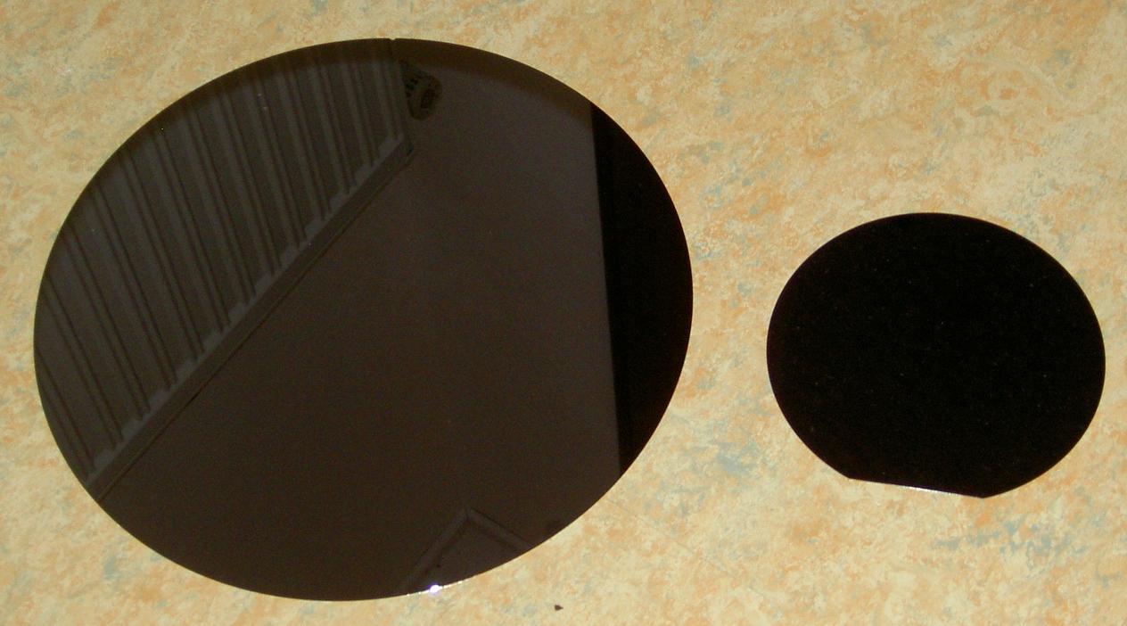
Wafer (electronics)
In electronics, a wafer (also called a slice or substrate) is a thin slice of semiconductor, such as a crystalline silicon (c-Si, silicium), used for the fabrication of integrated circuits and, in photovoltaics, to manufacture solar cells.
The wafer serves as the substrate for microelectronic devices built in and upon the wafer. It undergoes many microfabrication processes, such as doping, ion implantation, etching, thin-film deposition of various materials, and photolithographic patterning. Finally, the individual microcircuits are separated by wafer dicing and packaged as an integrated circuit.
In the semiconductor industry, the term wafer appeared in the 1950s to describe a thin round slice of semiconductor material, typically germanium or silicon. The round shape characteristic of these wafers comes from single-crystal ingots usually produced using the Czochralski method. Though, silicon wafers were first introduced in the 1940s.
By 1960, silicon wafers were being manufactured in the U.S. by companies such as MEMC and SunEdison. In 1965, American engineers Eric O. Ernst, Donald J. Hurd, and Gerard Seeley, while working under IBM, filed Patent US3423629A for the first high-capacity epitaxial apparatus.
Wafers are formed of highly pure, nearly defect-free single crystalline material, with a purity of 99.9999999% (9N) or higher. One process for forming crystalline wafers is known as the Czochralski method, invented by Polish chemist Jan Czochralski. In this process, a cylindrical ingot of high purity monocrystalline semiconductor, such as silicon or germanium, called a boule, is formed by pulling a seed crystal from a melt. Donor impurity atoms, such as boron or phosphorus in the case of silicon, can be added to the molten intrinsic material in precise amounts in order to dope the crystal, thus changing it into an extrinsic semiconductor of n-type or p-type.
The boule is then sliced with a wafer saw (a type of wire saw), machined to improve flatness, chemically etched to remove crystal damage from machining steps and finally polished to form wafers. The size of wafers for photovoltaics is 100–200 mm square and the thickness is 100–500 μm. Electronics use wafer sizes from 100 to 450 mm diameter. The largest wafers made have a diameter of 450 mm, but are not yet in general use.
Wafers are cleaned with weak acids to remove unwanted particles. There are several standard cleaning procedures to make sure the surface of a silicon wafer contains no contamination. One of the most effective methods is the RCA clean. When used for solar cells, the wafers are textured to create a rough surface to increase surface area and so their efficiency. The generated PSG (phosphosilicate glass) is removed from the edge of the wafer in the etching.
Silicon wafers are available in a variety of diameters from 25.4 mm (1 inch) to 300 mm (11.8 inches). Semiconductor fabrication plants, colloquially known as fabs, are defined by the diameter of wafers that they are tooled to produce. The diameter has gradually increased to improve throughput and reduce cost with the current state-of-the-art fab using 300 mm, with a proposal to adopt 450 mm. Intel, TSMC, and Samsung were separately conducting research to the advent of 450 mm "prototype" (research) fabs, though serious hurdles remain.
Hub AI
Wafer (electronics) AI simulator
(@Wafer (electronics)_simulator)
Wafer (electronics)
In electronics, a wafer (also called a slice or substrate) is a thin slice of semiconductor, such as a crystalline silicon (c-Si, silicium), used for the fabrication of integrated circuits and, in photovoltaics, to manufacture solar cells.
The wafer serves as the substrate for microelectronic devices built in and upon the wafer. It undergoes many microfabrication processes, such as doping, ion implantation, etching, thin-film deposition of various materials, and photolithographic patterning. Finally, the individual microcircuits are separated by wafer dicing and packaged as an integrated circuit.
In the semiconductor industry, the term wafer appeared in the 1950s to describe a thin round slice of semiconductor material, typically germanium or silicon. The round shape characteristic of these wafers comes from single-crystal ingots usually produced using the Czochralski method. Though, silicon wafers were first introduced in the 1940s.
By 1960, silicon wafers were being manufactured in the U.S. by companies such as MEMC and SunEdison. In 1965, American engineers Eric O. Ernst, Donald J. Hurd, and Gerard Seeley, while working under IBM, filed Patent US3423629A for the first high-capacity epitaxial apparatus.
Wafers are formed of highly pure, nearly defect-free single crystalline material, with a purity of 99.9999999% (9N) or higher. One process for forming crystalline wafers is known as the Czochralski method, invented by Polish chemist Jan Czochralski. In this process, a cylindrical ingot of high purity monocrystalline semiconductor, such as silicon or germanium, called a boule, is formed by pulling a seed crystal from a melt. Donor impurity atoms, such as boron or phosphorus in the case of silicon, can be added to the molten intrinsic material in precise amounts in order to dope the crystal, thus changing it into an extrinsic semiconductor of n-type or p-type.
The boule is then sliced with a wafer saw (a type of wire saw), machined to improve flatness, chemically etched to remove crystal damage from machining steps and finally polished to form wafers. The size of wafers for photovoltaics is 100–200 mm square and the thickness is 100–500 μm. Electronics use wafer sizes from 100 to 450 mm diameter. The largest wafers made have a diameter of 450 mm, but are not yet in general use.
Wafers are cleaned with weak acids to remove unwanted particles. There are several standard cleaning procedures to make sure the surface of a silicon wafer contains no contamination. One of the most effective methods is the RCA clean. When used for solar cells, the wafers are textured to create a rough surface to increase surface area and so their efficiency. The generated PSG (phosphosilicate glass) is removed from the edge of the wafer in the etching.
Silicon wafers are available in a variety of diameters from 25.4 mm (1 inch) to 300 mm (11.8 inches). Semiconductor fabrication plants, colloquially known as fabs, are defined by the diameter of wafers that they are tooled to produce. The diameter has gradually increased to improve throughput and reduce cost with the current state-of-the-art fab using 300 mm, with a proposal to adopt 450 mm. Intel, TSMC, and Samsung were separately conducting research to the advent of 450 mm "prototype" (research) fabs, though serious hurdles remain.