Recent from talks
Nothing was collected or created yet.
2N2222
View on Wikipedia


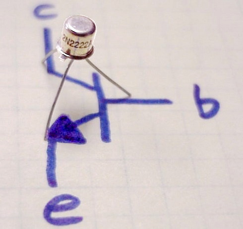
The 2N2222 is a common NPN bipolar junction transistor (BJT) used for general purpose low-power amplifying or switching applications. It is designed for low to medium current, low power, medium voltage, and can operate at moderately high speeds. It was originally made in the TO-18 metal can as shown in the picture.
The 2N2222 is considered a very common transistor,[1][2][3] and is used as an exemplar of an NPN transistor. It is frequently used as a small-signal transistor,[4][5] and it remains a small general purpose transistor[6] of enduring popularity.[7][8][9]
The 2N2222 was part of a family of devices described by Motorola at a 1962 IRE convention.[10] Since then it has been made by many semiconductor companies, for example, Texas Instruments.[11]
Specifications
[edit]The JEDEC registration of a device number ensures particular rated values will be met by all parts offered under that number. JEDEC registered parameters include outline dimensions, small-signal current gain, transition frequency, maximum values for voltage withstand, current rating, power dissipation and temperature rating, and others, measured under standard test conditions. Other part numbers will have different parameters. The exact specifications depend on the manufacturer, case type, and variation. Therefore, it is important to refer to the datasheet for the exact part number and manufacturer.
| Manufacturer | Vce | Ic | Ptot | fT |
|---|---|---|---|---|
| ST Microelectronics[12] 2N2222A |
40 V | 600 mA | 500 mW (Tamb ≤ 25 °C) 1.8 W (Tc ≤ 25 °C) |
300 MHz |
All variations have a beta or current gain (hfe) of at least 100 in optimal conditions. It is used in a variety of analog amplification and switching applications.
Other switching transistors
[edit]
NPN silicon transistors with similar properties are also made in a variety of small through-hole and surface mount packages including TO-92, SOT-23, and SOT-223.
Replacements for the 2N2222 are commonly available in the cheaper TO-92 packaging, where it is known as the PN2222 or P2N2222, which has similar specifications except for the lower maximum collector current.[13] The P2N2222 has a different order of pins than the metal case 2N2222, with its emitter and collector connections switched; other plastic-case transistors also have different pinouts.
Single transistors are also available in several different surface mount packages, and a number of manufacturers market surface mount packages that incorporate several 2N2222-type transistors in one package as an array of transistors. The general specifications of the various variants are similar, with the biggest difference being the maximum allowable current and power dissipation.
The BC548 family, including the BC547A to BC550C, are lower voltage, lower current, general-purpose transistors in TO-92 packages, originating in Europe, that are often found in small-signal amplification and switching circuits of the type where the 2N2222 might otherwise be used. They are not true replacements, but comparable devices that may be substituted only in circuits where the maximum current and voltage ratings are not exceeded.
The 2N2907 is an equally popular PNP transistor complementary to the 2N2222.[14]
The 2N3904 is an NPN transistor that can only switch one-third the current of the 2N2222 but has otherwise similar characteristics. The 2N3904 exhibits its forward gain (beta) peak at a lower current than the 2N2222, and is useful in amplifier applications with reduced Ic, e.g., (gain peak at 10 mA for the 2N3904 but 150 mA for the 2N2222).
A version of the 2N2222A in a larger metal TO-39 case, the 2N2219A had a higher power dissipation rating (3 watts when attached to a heatsink that keeps the case temperature at 25 C, or 0.8 watts in free air, compared with only 1.8 watts and 0.5 watts (respectively) for the 2N2222A.[12]
Part numbers
[edit]The 2N2222 (NPN) and 2N2907 (PNP) are complementary transistor pairs.[15] The prefix of each part number varies for each physical package type.
| BJT | Thru-hole | Surface-mount | ||
|---|---|---|---|---|
| TO-18 | TO-92 | SOT23 | SOT223 | |
| NPN | 2N2222 | PN2222 | MMBT2222 | PZT2222A |
| PNP | 2N2907 | PN2907 | MMBT2907 | PZT2907A |
See also
[edit]References
[edit]- ^ Dan O'Sullivan, Tom Igoe; "Physical Computing"; Cengage Learning; pp.19; 2004; ISBN 1-59200-346-X
- ^ Brad Graham, Kathy McGowan; "Mind Performance Projects for the Evil Genius"; McGraw Hill Professional; pp.18; 2010; ISBN 978-0-07-162392-6
- ^ Brad Graham, Kathy McGowan; "51 High-Tech Practical Jokes for the Evil Genius"; McGraw Hill Professional; pp.12; 2007; ISBN 978-0-07-149494-6
- ^ Gordon McComb; "The Robot Builder's Bonanza"; McGraw-Hill Professional; 2001; pp.261; ISBN 978-0-07-136296-2
- ^ William Rynone; "Linear Active Circuits — Design and Analysis"; Artech House; pp.19; 1986; ISBN 0-89006-199-8
- ^ Dennis Barnaal, "Analog and Digital Electronics for Scientific Application"; Breton Publishers; pp.301; 1982; ISBN 0-534-01044-X
- ^
Rudolf F. Graf and William Sheets (2001). Build your own low-power transmitters: projects for the electronics experimenter. Newnes. p. 14. ISBN 978-0-7506-7244-3.
The 2N2222, 2N2905, and 2N3055 devices, for example, which date back to the 1960s but have been improved, are still useful in new designs and are still popular for experimenters.
- ^
Ed Da Silva (2001). High frequency and microwave engineering. Newnes. p. 263. ISBN 978-0-7506-5046-5.
Typical examples are the well known NPN and PNP industrial and military types, 2N2222 and 2N2907, which have been used for over four decades and are still being used in many designs.
- ^
Jack Ward. "THE DEVELOPMENT OF THE 2N2222: The Most Successful and Widely Used Transistor Ever Developed!". The Transistor Museum. Archived from the original on 14 April 2011. Retrieved 26 March 2011.
Since its initial product launch by Motorola at the 1962 IRE Convention, the 2N2222 has become the most widely used and universally recognized transistor of all time. Billions of units have been manufactured over the past 45 years and there is continuing high volume annual production.
- ^ http://www.semiconductormuseum.com/Transistors/Motorola/Haenichen/Haenichen_Page11.htm Haenichen oral history retrieved from the Semiconductor Museum 2011 May 13
- ^ The Transistor and Diode Data Book for Design Engineers, Texas Instruments Incorporated, no date, TI publication number CC413 71242-73-CSS, page 4-93
- ^ a b "2N2219A, 2N2222A High Speed Switches" (PDF). STMicroelectronics. February 2022. Archived (PDF) from the original on 31 March 2022. Retrieved 8 April 2022.
- ^ http://www.fairchildsemi.com/ds/PN/PN2222.pdf Archived 27 September 2007 at the Wayback Machine Retrieved 3 June 2012
- ^
Dave Hrynkiw and Mark W. Tilden (2002). Junkbots, bugbots, and bots on wheels: building simple robots with BEAM technology. McGraw-Hill Professional. p. 44. ISBN 978-0-07-222601-0.
Learn to keep an eye open for the following transistors, as they're among the most useful, inexpensive, and popular types: PN2222/PN2907 These are general-purpose NPN/PNP transistors that can drive some good amounts of power. They're listed together because they're complementary transistors.
- ^ "2N2907 & 2N2907A datasheet" (PDF). Comset Semiconductors. Archived (PDF) from the original on 19 August 2019. Retrieved 7 July 2022.
Further reading
[edit]- Historical Databooks
- Semiconductor Data Book, 916 pages, 1965, Motorola.
- Small-Signal Semiconductors Data Book, 1218 pages, 1987, Motorola.
- Transistor and Diode Data Book, 1258 pages, 1973, Texas Instruments.
External links
[edit]- Datasheet for 2N2222A Hi-reliability equivalent (PDF) by Microsemi
- Datasheet for Fairchild Semiconductor's equivalent PN2222 (PDF)
- 2N2222 Transistor History, Packaging and Datasheet
- The Fascinating Geometry of Transistors, video explaining the geometry of an actual 2N2222.
2N2222
View on GrokipediaOverview
Description
The 2N2222 is a low-power NPN bipolar junction transistor (BJT) designed for amplification and switching in low- to medium-current applications.[6] It features a silicon planar epitaxial structure housed typically in a TO-18 metal can package, enabling reliable performance in general-purpose electronics.[5] First specified in 1962 by Motorola as a military-grade component, it has become a standard device due to its versatility and robustness.[7] In basic operation, the 2N2222 functions as a current-controlled device where a small input current at the base-emitter junction regulates a much larger collector-emitter current. The forward-biased base-emitter junction allows majority carriers (electrons in NPN) to diffuse from the emitter to the base, while the reverse-biased base-collector junction collects these carriers, amplifying the signal. The transistor supports four operating modes: forward-active for linear amplification, saturation for low-resistance switching, cutoff for blocking current, and reverse-active for specialized low-gain scenarios. Key advantages include a high DC current gain (hFE) typically ranging from 100 to 300, enabling efficient signal amplification with minimal base drive, and fast switching capabilities with a transition frequency (fT) around 250–300 MHz, supporting high-speed applications.[6][5] Its proven reliability in diverse environments has made it a staple in both commercial and legacy military systems.[7]History
The 2N2222 transistor originated in the early 1960s as part of the U.S. military's Joint Army-Navy (JAN) specifications under MIL-PRF-19500, aimed at providing reliable silicon NPN switching transistors for defense electronics applications.[4] This standardization effort sought to ensure consistent performance in harsh environments, building on earlier germanium devices.[4] Introduced in 1962 by Motorola at the IRE convention in New York, the 2N2222 utilized innovative STAR (Silicon Transistor Annular Rugged) geometry developed by engineer Jack Haenichen, marking a shift to epitaxial silicon construction for improved speed and reliability.[8] It replaced earlier germanium transistors such as the 2N1304, offering superior thermal stability and higher frequency response suitable for both military and emerging commercial needs.[9] In the late 1960s, an improved variant, the 2N2222A, was introduced with higher voltage ratings (such as 40 V collector-emitter and 75 V collector-base) and lower saturation voltages (0.3 V at 150 mA collector current), broadening its applicability.[5] The 2N2222 series gained prominence in space programs through its radiation-hardened variants, tested for reliability in orbital environments, and proliferated in the 1970s consumer electronics boom for applications in radios, amplifiers, and early computing peripherals.[10] Military specifications advanced in the 1980s with the introduction of higher-assurance levels like JANTX2N2222A under updated JAN standards, emphasizing extended screening for mission-critical use.[4] As of 2025, the 2N2222 remains in continuous production by vendors including STMicroelectronics, Central Semiconductor, and Microchip Technology, benefiting from over six decades of backward compatibility that sustains its role in legacy and new designs.[11][12][13]Design and Construction
Semiconductor Structure
The 2N2222 is a silicon-based NPN bipolar junction transistor featuring a triple-layer semiconductor structure, consisting of an N-type emitter region, a P-type base region, and an N-type collector region, forming two PN junctions that enable its amplification and switching capabilities.[14] This configuration is achieved through a planar epitaxial fabrication process on a silicon substrate, where the layers are formed using diffusion or ion implantation techniques to precisely control dopant distribution.[1] In terms of doping, the emitter is heavily doped to promote high injection efficiency of charge carriers into the base, while the base is lightly doped relative to the emitter to minimize recombination and achieve high transconductance, and the collector is moderately doped to support voltage handling without excessive power dissipation. These doping profiles contribute to the transistor's current gain and frequency response. The base-emitter junction exhibits forward-biased diffusion capacitance, which dominates during operation and arises from stored charge in the base, while the collector-base junction shows reverse-biased depletion capacitance due to the space-charge region, both influencing the transition frequency (f_T) of approximately 250-300 MHz.[1] Typical values include input capacitance (C_{ib}) up to 25 pF and output capacitance (C_{ob}) up to 8 pF at specified test conditions.[15] The active silicon die measures about 0.35 mm × 0.35 mm (0.12 mm²), with aluminum metallization on the top side (1.3 μm thick) for emitter and base contacts and gold-arsenide on the back (0.9 μm thick) for the collector, subsequently encapsulated in hermetic metal (e.g., TO-18) or plastic (e.g., TO-92) packages for protection and handling.[15]Pin Configuration
The 2N2222 transistor, an NPN bipolar junction transistor, features a standardized pin configuration that varies slightly by package type to facilitate proper electrical connections in circuit designs. In the standard TO-18 metal can package, the pins are arranged as follows when viewed from the bottom (leads pointing away) with the flat side facing the viewer: Pin 1 is the emitter, Pin 2 is the base, and Pin 3 is the collector.[6][16] The collector is internally connected to the metal case, allowing for direct heat sinking through the package body in applications requiring thermal management.[16] For the TO-92 plastic package (often designated as the PN2222A variant, though functionally equivalent to the 2N2222A), the pinout is configured with the flat side facing the viewer: the left pin is the emitter, the middle pin is the base, and the right pin is the collector.[6] This orientation ensures consistent wiring across common through-hole mounting practices. In typical circuit implementations, the emitter pin is connected to ground or the common reference point, the base pin receives the input control signal to modulate transistor conduction, and the collector pin interfaces with the load, such as a resistor or another component.[6] For high-power operations approaching the maximum ratings, appropriate heat sinking is recommended, particularly for the TO-18 package where the case serves as the collector terminal.[6] The schematic symbol for the 2N2222 depicts a standard NPN transistor configuration, with an arrow on the emitter lead pointing outward to indicate current flow direction from collector to emitter in the active region.[6]| Package Type | View Orientation | Pin 1/Left | Pin 2/Middle | Pin 3/Right or Collector Case |
|---|---|---|---|---|
| TO-18 (Metal Can) | Bottom (leads away), flat side facing | Emitter | Base | Collector (also case) |
| TO-92 (Plastic) | Front, flat side facing | Emitter | Base | Collector |
Electrical Characteristics
Absolute Maximum Ratings
The absolute maximum ratings for the 2N2222A transistor (common variant) represent the extreme limits of operating conditions under which the device can be expected to perform reliably without permanent damage, as specified by the manufacturer. These ratings are critical for circuit designers to ensure safe operation and prevent failure modes such as thermal runaway or avalanche breakdown. They are typically measured at an ambient temperature of 25°C unless otherwise noted, and values may vary slightly by manufacturer and package type, but the following are standard guarantees for the TO-92 package.[1][5]| Parameter | Symbol | Value | Unit | Conditions/Notes |
|---|---|---|---|---|
| Collector-emitter voltage | VCEO | 40 | V | Open base (IB=0) |
| Collector-base voltage | VCBO | 75 | V | Open emitter (IE=0) |
| Emitter-base voltage | VEBO | 6 | V | Open collector (IC=0) |
| Collector current | IC | 600 | mA | Continuous (800 mA peak for short durations) |
| Total power dissipation | PD | 625 | mW | At TA=25°C, TO-92 package |
| Derating above 25°C | - | 5 | mW/°C | For ambient temperature |
| Thermal resistance, junction-to-ambient | θJA | 200 | °C/W | For TO-92 package |
| Operating junction temperature range | TJ | -55 to +150 | °C | - |
Typical Performance Parameters
The 2N2222A NPN bipolar junction transistor demonstrates reliable performance in amplification and switching applications through its key electrical parameters under normal operating conditions. The DC current gain, denoted as h_{FE}, has a minimum value of 35 at a collector current I_C of 0.1 mA and collector-emitter voltage V_{CE} of 10 V, increasing to a minimum of 75 at I_C = 10 mA under the same V_{CE}.[5] Typical h_{FE} values range from 100 to 300 across I_C from 0.1 mA to 150 mA at V_{CE} = 10 V, providing consistent gain for moderate current levels.[1] The transition frequency f_T, a measure of the transistor's small-signal bandwidth, achieves a minimum of 300 MHz at I_C = 20 mA, V_{CE} = 20 V, and test frequency of 100 MHz, enabling high-frequency operation up to VHF ranges.[1] In saturation mode, the collector-emitter saturation voltage V_{CE(sat)} is limited to a maximum of 0.3 V at I_C = 150 mA and base current I_B = 15 mA, minimizing power loss in switching circuits.[5] Output admittance h_{OE}, which reflects the transistor's output impedance, has a maximum of 35 μS at I_C = 1 mA and 200 μS at I_C = 10 mA, with V_{CE} = 10 V and f = 1 kHz, corresponding to output resistances of approximately 28 kΩ and 5 kΩ, respectively, for small-signal analysis.[1] The noise figure is low, reaching a maximum of 4 dB at I_C = 100 μA, V_{CE} = 10 V, source resistance R_S = 1 kΩ, and frequency of 1 kHz, making it suitable for low-noise audio amplification.[1] Additionally, the temperature coefficient of h_{FE} is approximately -1%/°C, indicating a gradual decrease in gain with rising temperature as shown in manufacturer characterization graphs.[1]| Parameter | Typical Value | Conditions | Source |
|---|---|---|---|
| h_{FE} (DC current gain) | 100–300 | I_C = 0.1–150 mA, V_{CE} = 10 V | ON Semiconductor datasheet[1] |
| f_T (transition frequency) | ≥300 MHz | I_C = 20 mA, V_{CE} = 20 V, f = 100 MHz | ON Semiconductor datasheet[1] |
| V_{CE(sat)} (saturation voltage) | ≤0.3 V | I_C = 150 mA, I_B = 15 mA | STMicroelectronics datasheet[5] |
| h_{OE} (output admittance) | Max 35–200 μS | I_C = 1–10 mA, V_{CE} = 10 V, f = 1 kHz | ON Semiconductor datasheet[1] |
| Noise figure | ≤4 dB | I_C = 100 μA, V_{CE} = 10 V, R_S = 1 kΩ, f = 1 kHz | ON Semiconductor datasheet[1] |
Applications
Switching Circuits
The 2N2222 transistor serves as an effective low-side switch in digital circuits, with its base driven directly by logic-level signals such as 5 V TTL outputs to control loads drawing up to 600 mA (pulsed up to 800 mA), including relays, LEDs, and small motors.[17][5] In this configuration, the transistor connects the load to ground when saturated, enabling efficient on/off operation while minimizing power dissipation in the control logic.[17] Key to its switching performance are the characteristic times: a delay time of approximately 10 ns, rise time of 25 ns, and fall time of 60 ns, typically measured under conditions of VCC = 30 V, IC = 150 mA, and IB = 15 mA.[1] These fast transitions support reliable operation in time-sensitive applications. The device's high transition frequency (fT) of 300 MHz further enables its use in pulse generators and choppers, where switching frequencies up to 100 MHz can be achieved for RF and high-speed modulation tasks.[5] To ensure saturation and low VCE(sat), the base drive current must satisfy IB ≥ IC / hFE_min, with hFE_min typically 100 at IC = 150 mA and VCE = 10 V.[17] When switching inductive loads, such as relays, a snubber circuit—often an RC network across the collector-emitter— is recommended to suppress voltage spikes and protect against transients.Amplification Circuits
The 2N2222 transistor is widely employed in common-emitter amplifier configurations for linear signal amplification, providing voltage gain while inverting the input signal. In this setup, the voltage gain is approximately , where is the transconductance, is the collector current, and mV is the thermal voltage at 25°C.[18] This configuration leverages the transistor's typical current gain of 100 to 300 at moderate collector currents, enabling effective amplification of small signals with a collector resistor selected for desired gain and load matching.[17] It is particularly suitable for audio applications, supporting bandwidths up to 20 kHz without significant distortion in low-power designs.[19] For applications requiring higher current gain, such as interfacing with low-output sensors, a Darlington pair can be formed using two 2N2222 transistors, where the collector-emitter path of the first drives the base of the second. This arrangement multiplies the individual values, yielding an effective gain exceeding 10,000 (based on minimum per transistor), while maintaining the voltage rating but increasing the saturation voltage.[17] The Darlington configuration enhances sensitivity for weak signal amplification but introduces higher base-emitter voltage drop, typically around 1.2 V. In radio-frequency (RF) amplification, the 2N2222 operates effectively up to the VHF band (30–300 MHz), owing to its transition frequency of 250–300 MHz, which defines the upper limit for useful gain.[5] It finds use in low-power oscillators and mixers, where impedance matching networks ensure maximum power transfer and minimize reflections.[2] Stable operation in these amplification circuits relies on proper biasing techniques, such as the voltage divider method applied to the base, which provides temperature-independent quiescent point setting by drawing current through resistors much larger than the base current.[19] Additionally, AC coupling via capacitors at input and output stages prevents DC offsets from propagating in multi-stage amplifiers, preserving signal integrity.Variants and Packaging
Part Number Variations
The 2N2222 transistor originated as a military-grade device under the Joint Army-Navy (JAN) specification, introduced by Motorola in 1962 for high-speed switching applications in hermetic TO-18 packages.[7] This version met the requirements of MIL-PRF-19500/255, establishing baseline performance for NPN silicon switching transistors with collector currents up to 800 mA.[17] The 2N2222A variant emerged as a commercial upgrade, featuring enhanced voltage ratings such as VCEO up to 40 V (compared to 30 V for the original 2N2222), with DC current gain (hFE) ranging from 35 to 300—similar to the original.[6][5] It also received CECC 50002-101 approval for European standards, ensuring compatibility in regulated amplification and switching circuits. Motorola's MPS2222 serves as a commercial equivalent to the 2N2222, maintaining similar electrical characteristics including a 30 V VCEO and 600 mA IC maximum, but optimized for plastic TO-92 packaging to reduce costs in non-military applications.[20] The PN2222 and PN2222A are common plastic-packaged (TO-92) equivalents to the 2N2222 and 2N2222A, respectively, with matching electrical specifications including VCEO of 40 V and IC up to 800 mA, widely used in general-purpose and hobbyist applications.[1] Within the same family, the 2N2219 and 2N2221 represent related types with similar power handling (Pd 500 mW, IC 800 mA), but the 2N2221 has a lower VCEO of 30 V compared to 40 V for the 2N2222, suiting applications with reduced voltage requirements. The 2N2219A offers VCEO of 40 V for medium-power switching.[5] Certifications for the 2N2222 series include qualification under MIL-PRF-19500 for military reliability, with RoHS compliance achieved in lead-free finishes starting in 2006 to meet EU environmental directives.[17][21] For space and high-reliability uses, screening levels such as MIL-STD-883 Class B are applied, including thermal cycling and radiation hardness assurance up to JANTXV levels.[22]Package Types and Dimensions
The 2N2222 transistor is available in several package types, each suited to different assembly and environmental requirements, with the TO-18 metal can providing robust hermetic sealing for high-reliability applications such as military and aerospace systems.[16] The TO-18 package features a cylindrical metal enclosure with a diameter of approximately 5.08 mm and a lead diameter of 0.41 mm, spaced at 2.54 mm center-to-center, enabling through-hole mounting while offering a junction-to-case thermal resistance (θJC) of 83.3 °C/W for efficient heat dissipation in demanding conditions.[17] Constructed from steel with glass-to-metal seals, it weighs about 0.7 g, contributing to its durability in harsh environments. For cost-sensitive, general-purpose designs, the TO-92 plastic package is widely used, featuring a molded flame-retardant epoxy body with a height of 5.2 mm maximum and a lead pitch of 1.27 mm for straightforward through-hole PCB insertion.[1] This package has a higher junction-to-ambient thermal resistance (θJA) of 200 °C/W, limiting its power handling without additional cooling, and weighs approximately 0.2 g, making it lightweight for consumer electronics.[1] Surface-mount applications benefit from the SOT-23 variant (often designated MMBT2222A), which offers a compact 2.9 mm × 1.3 mm footprint ideal for dense PCB layouts in modern compact devices, with adoption growing in the 1990s alongside the rise of SMD technology. This plastic-encapsulated package supports automated assembly but requires careful thermal management due to its smaller size and higher θJA, typically around 250 °C/W.| Package Type | Key Dimensions | Thermal Resistance | Material | Approximate Weight |
|---|---|---|---|---|
| TO-18 (Metal Can) | Diameter: 5.08 mm; Lead spacing: 2.54 mm | θJC: 83.3 °C/W | Steel with glass seals | 0.7 g |
| TO-92 (Plastic) | Height: 5.2 mm; Lead pitch: 1.27 mm | θJA: 200 °C/W | Flame-retardant epoxy | 0.2 g |
| SOT-23 (SMD) | Footprint: 2.9 × 1.3 mm | θJA: 250 °C/W | Plastic | <0.1 g |
