Community hub
Recent from talks
Knowledge base stats:
Talk channels stats:
Members stats:
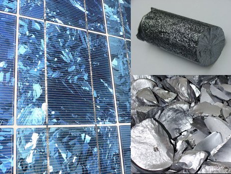
Polycrystalline silicon
Polycrystalline silicon, or multicrystalline silicon, also called polysilicon, poly-Si, or mc-Si, is a high purity, polycrystalline form of silicon, used as a raw material by the solar photovoltaic and electronics industry.
Polysilicon is produced from metallurgical grade silicon by a chemical purification process, called the Siemens process. This process involves distillation of volatile silicon compounds, and their decomposition into silicon at high temperatures. An emerging, alternative process of refinement uses a fluidized bed reactor, which is lower cost. The photovoltaic industry also produces upgraded metallurgical-grade silicon (UMG-Si), using metallurgical instead of chemical purification processes for lower cost at the expense of purity. When produced for the electronics industry, polysilicon contains impurity levels of less than one part per billion (ppb), while polycrystalline solar grade silicon (SoG-Si) is generally less pure. In the 2010's, production shifted toward China, with China-based companies accounting for seven of the top ten producers and around 90% of total worldwide production capacity of approximately 1,400,000 MT. German, US and South Korea companies account for the remainder.
The polysilicon feedstock – large rods from the Siemens process, usually broken into chunks of specific sizes and packaged in clean rooms before shipment – is directly cast into multicrystalline ingots which are large square blocks weighing around 800 kg for making solar wafers or submitted as-is to a recrystallization process to grow single crystal boules usually with the Czochralski method. The boules are then sliced into thin silicon wafers and used for the production of solar cells, integrated circuits and other semiconductor devices.
Polysilicon consists of small crystals, also known as crystallites, giving the material its typical metal flake effect. While polysilicon and multisilicon are often used as synonyms, multicrystalline usually refers to crystals larger than one millimetre. Multicrystalline solar cells are the most common type of solar cells in the fast-growing PV market and consume most of the worldwide produced polysilicon. About 5 tons of polysilicon is required to manufacture one 1 megawatt (MW) of conventional solar modules.[citation needed] Polysilicon is distinct from monocrystalline silicon and amorphous silicon.
In single-crystal silicon, also known as monocrystalline silicon, the crystalline framework is homogeneous, which can be recognized by an even external colouring. The entire sample is one single, continuous and unbroken crystal as its structure contains no grain boundaries. Large single crystals are rare in nature and can also be difficult to produce in the laboratory (see also recrystallisation). In contrast, in an amorphous structure the order in atomic positions is limited to short range.
Polycrystalline and paracrystalline phases are composed of a number of smaller crystals or crystallites. Polycrystalline silicon (or semi-crystalline silicon, polysilicon, poly-Si, or simply "poly") is a material consisting of multiple small silicon crystals. Polycrystalline cells can be recognized by a visible grain, a "metal flake effect". Semiconductor grade (also solar grade) polycrystalline silicon is converted to single-crystal silicon – meaning that the randomly associated crystallites of silicon in polycrystalline silicon are converted to a large single crystal. Single-crystal silicon is used to manufacture most Si-based microelectronic devices. Polycrystalline silicon can be as much as 99.9999% pure. Ultra-pure poly is used in the semiconductor industry, starting from poly rods that are two to three meters in length resulting from the Siemens process. In the microelectronics industry (semiconductor industry), poly is used at both the macro and micro scales. Single crystals are grown using the Czochralski, zone melting and Bridgman–Stockbarger methods. The Czochralski method often uses polysilicon as the starting material.
At the component level, polysilicon has long been used as the conducting gate material in MOSFET and CMOS processing technologies. For these technologies, it is deposited using low-pressure chemical-vapour deposition (LPCVD) reactors at high temperatures and is usually heavily doped n-type or p-type.
More recently, intrinsic and doped polysilicon is being used in large-area electronics as the active and/or doped layers in thin-film transistors. Although it can be deposited by LPCVD, plasma-enhanced chemical vapour deposition (PECVD), or solid-phase crystallization of amorphous silicon in certain processing regimes, these processes still require relatively high temperatures of at least 300 °C. These temperatures make deposition of polysilicon possible for glass substrates but not for plastic substrates.
Hub AI
Polycrystalline silicon AI simulator
(@Polycrystalline silicon_simulator)
Polycrystalline silicon
Polycrystalline silicon, or multicrystalline silicon, also called polysilicon, poly-Si, or mc-Si, is a high purity, polycrystalline form of silicon, used as a raw material by the solar photovoltaic and electronics industry.
Polysilicon is produced from metallurgical grade silicon by a chemical purification process, called the Siemens process. This process involves distillation of volatile silicon compounds, and their decomposition into silicon at high temperatures. An emerging, alternative process of refinement uses a fluidized bed reactor, which is lower cost. The photovoltaic industry also produces upgraded metallurgical-grade silicon (UMG-Si), using metallurgical instead of chemical purification processes for lower cost at the expense of purity. When produced for the electronics industry, polysilicon contains impurity levels of less than one part per billion (ppb), while polycrystalline solar grade silicon (SoG-Si) is generally less pure. In the 2010's, production shifted toward China, with China-based companies accounting for seven of the top ten producers and around 90% of total worldwide production capacity of approximately 1,400,000 MT. German, US and South Korea companies account for the remainder.
The polysilicon feedstock – large rods from the Siemens process, usually broken into chunks of specific sizes and packaged in clean rooms before shipment – is directly cast into multicrystalline ingots which are large square blocks weighing around 800 kg for making solar wafers or submitted as-is to a recrystallization process to grow single crystal boules usually with the Czochralski method. The boules are then sliced into thin silicon wafers and used for the production of solar cells, integrated circuits and other semiconductor devices.
Polysilicon consists of small crystals, also known as crystallites, giving the material its typical metal flake effect. While polysilicon and multisilicon are often used as synonyms, multicrystalline usually refers to crystals larger than one millimetre. Multicrystalline solar cells are the most common type of solar cells in the fast-growing PV market and consume most of the worldwide produced polysilicon. About 5 tons of polysilicon is required to manufacture one 1 megawatt (MW) of conventional solar modules.[citation needed] Polysilicon is distinct from monocrystalline silicon and amorphous silicon.
In single-crystal silicon, also known as monocrystalline silicon, the crystalline framework is homogeneous, which can be recognized by an even external colouring. The entire sample is one single, continuous and unbroken crystal as its structure contains no grain boundaries. Large single crystals are rare in nature and can also be difficult to produce in the laboratory (see also recrystallisation). In contrast, in an amorphous structure the order in atomic positions is limited to short range.
Polycrystalline and paracrystalline phases are composed of a number of smaller crystals or crystallites. Polycrystalline silicon (or semi-crystalline silicon, polysilicon, poly-Si, or simply "poly") is a material consisting of multiple small silicon crystals. Polycrystalline cells can be recognized by a visible grain, a "metal flake effect". Semiconductor grade (also solar grade) polycrystalline silicon is converted to single-crystal silicon – meaning that the randomly associated crystallites of silicon in polycrystalline silicon are converted to a large single crystal. Single-crystal silicon is used to manufacture most Si-based microelectronic devices. Polycrystalline silicon can be as much as 99.9999% pure. Ultra-pure poly is used in the semiconductor industry, starting from poly rods that are two to three meters in length resulting from the Siemens process. In the microelectronics industry (semiconductor industry), poly is used at both the macro and micro scales. Single crystals are grown using the Czochralski, zone melting and Bridgman–Stockbarger methods. The Czochralski method often uses polysilicon as the starting material.
At the component level, polysilicon has long been used as the conducting gate material in MOSFET and CMOS processing technologies. For these technologies, it is deposited using low-pressure chemical-vapour deposition (LPCVD) reactors at high temperatures and is usually heavily doped n-type or p-type.
More recently, intrinsic and doped polysilicon is being used in large-area electronics as the active and/or doped layers in thin-film transistors. Although it can be deposited by LPCVD, plasma-enhanced chemical vapour deposition (PECVD), or solid-phase crystallization of amorphous silicon in certain processing regimes, these processes still require relatively high temperatures of at least 300 °C. These temperatures make deposition of polysilicon possible for glass substrates but not for plastic substrates.