Hubbry Logo
Socket 4Socket 4Main
Open search
Socket 4
Community hub
Socket 4
logo
8 pages, 0 posts
0 subscribers
Be the first to start a discussion here.
Socket 4
Socket 4
from Wikipedia
Socket 4
TypeZIF
Chip form factorsPPGA
Contacts273
FSB protocol?
FSB frequency60, 66 MT/s
Voltage range5 V
ProcessorsIntel P5 Pentium
PredecessorSocket 3
SuccessorSocket 5

This article is part of the CPU socket series

Socket 4, presented in 1993, was the first CPU socket designed for the early P5 Pentium microprocessors. Socket 4 was the only 5-volt socket for the Pentium. Socket 4 does support a special Pentium OverDrive, which allows running at 120 MHz (for the 60 MHz Pentium) or 133 MHz (for the 66 MHz Pentium).[1]

Socket 4 was superseded by the 3.3-volt-powered Socket 5 in 1994.

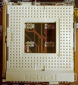
A socket 4 processor mounted on a motherboard

See also

[edit]

References

[edit]
Revisions and contributorsEdit on WikipediaRead on Wikipedia
from Grokipedia
Socket 4 is a 273-pin (ZIF) CPU socket introduced by in 1993 for its first-generation microprocessors, specifically the 60 MHz and 66 MHz models, marking the debut of the Pentium brand in personal computing. Operating at a 5 V supply voltage, it features a (PGA) design with a 64-bit external bus and supports speeds of 60 MHz or 66 MHz to match the processors' clock rates. The socket's ZIF lever mechanism facilitates damage-free processor installation and upgrades, with 52 power (Vcc) and 49 ground (Vss) pins ensuring stable electrical connections. Compatible exclusively with early Pentium processors, Socket 4 accommodates the original 60/66 MHz s fabricated on a 0.8 μm process, as well as the 1996 upgrades running at 120/133 MHz internally while preserving external 60/66 MHz bus compatibility through an on-chip that steps down to 3.3 V for the core. These OverDrive processors, also in a 273-pin PGA package, deliver approximately double the performance of the originals without requiring motherboard modifications, supporting power draws up to 3.2 A at 66 MHz. The socket's design emphasized reliability for desktop systems, including provisions for fan heatsinks powered via connectors. As 's initial socket for the superscalar P5 architecture, Socket 4 played a pivotal role in the mid-1990s PC transition from 486-era systems, but its 5 V-only limitation and lack of scalability led to rapid obsolescence by 1994, supplanted by the more versatile 3.3 V-compatible Socket 5 and for higher-speed s. Today, it remains a historical artifact of early , collectible among retro hardware enthusiasts for its role in enabling the first widespread adoption of dual-integer pipelines and integrated floating-point units in consumer CPUs.

Overview

Introduction

Socket 4 is a (ZIF) CPU socket developed by as the first dedicated interface for the early P5 microprocessors. Introduced in 1993, it marked a shift from the pin-compatible designs of previous generations, providing a standardized mounting solution optimized for the Pentium's (PGA) package. This socket played a pivotal role in transitioning PC systems from the 486 architecture to the more advanced Pentium design, facilitating the adoption of superscalar execution and elevated clock speeds that significantly boosted performance over prior processors. As the successor to , which primarily supported 486 CPUs, Socket 4 enabled manufacturers to build platforms tailored to the Pentium's requirements without relying on adapters. Socket 4 was released alongside Intel's inaugural processors—the 60 MHz and 66 MHz models—on March 22, 1993, ushering in the fifth generation of x86 processors and accelerating the evolution of personal computing.

Key features

Socket 4 operates exclusively with a 5 V voltage supply, a design choice that ensured compatibility with the original processors but rendered it incompatible with subsequent 3.3 V Pentiums without specialized voltage adapter modules or interposers. This 5 V requirement stems from the electrical specifications of the early P5 architecture, where the processor core and I/O interfaces both drew power from the same rail. The socket supports (FSB) speeds of 60 MT/s and 66 MT/s, directly aligned with the core clock frequencies of the supported processors to maintain synchronous operation. It utilizes a 273-pin (PGA) form factor, which includes a keyed orientation via a chamfered corner on the processor package to prevent misinsertion and ensure proper alignment in the (ZIF) mechanism. Due to inherent thermal dissipation limits—such as a maximum case of 80°C for the 60 MHz variant and 70°C for the 66 MHz—and electrical constraints on power delivery, Socket 4 lacks support for higher voltages or bus speeds beyond 66 MHz, capping its scalability compared to later sockets. These limitations highlighted the transitional nature of the socket, prioritizing reliability for early desktop systems over future-proofing.

Technical specifications

Electrical characteristics

Socket 4 operates exclusively at a fixed supply voltage of 5 V ± 5%, distinguishing it from subsequent sockets like Socket 5, which supported 3.3 V processors. This single-voltage design aligns with the requirements of the original processors, ensuring compatibility without the need for onboard . Input low voltage ranges from -0.3 V to 0.8 V, while input high voltage spans 2.0 V to Vcc + 0.3 V, maintaining signal integrity under the 5 V environment. The (FSB) frequency is synchronized 1:1 with the CPU clock, limited to 60 MT/s for the 60 MHz Pentium and 66 MT/s for the 66 MHz variant, providing the fundamental timing for data transfers. This configuration supports a 32-bit address bus (A31–A3) for memory addressing and a 64-bit data bus (D63–D0) for high-bandwidth operations, inheriting the superscalar architecture's bus structure while adhering to Socket 4's pinout. Power consumption reflects the era's technology, with typical values of 11.9 W (2370 mA) at 60 MHz and 13 W (2600 mA) at 66 MHz, rising to maximums of 14.6 W (2910 mA) and 16 W (3200 mA), respectively; notably, no features such as dynamic voltage scaling or clock throttling are implemented, relying instead on basic (SMM) for interrupts via SMI# and SMIACT# pins. Socket 4's design emphasizes robust signal integrity through dedicated pin assignments, allocating 52 pins to Vcc (e.g., A04, A05, A06) and 49 pins to ground (Vss; e.g., B05, B06, B07) to distribute power evenly and minimize noise across the 273-pin grid. These assignments, combined with output specifications like 0.45 V low at 4 mA and 2.4 V high at 1 mA, ensure reliable operation without the multi-voltage flexibility of later sockets.

Mechanical design

Socket 4 features a (PGA) configuration with 273 contacts arranged in a 21×21 grid, where positions are intentionally omitted including two for keying to ensure correct processor orientation during installation. The socket employs a (ZIF) design, incorporating a lever-actuated mechanism that lifts the retention contacts, allowing the processor to be placed without or stressing the pins, followed by secure locking for reliable electrical connection. It is mounted directly onto the using , facilitating integration into the PCB layout. Measuring approximately 2.25 inches square, the socket aligns with the dimensions of compatible Pentium processors and fits standard AT form factor motherboards, enabling straightforward upgrades in contemporary PC chassis of the era. To enhance longevity and conductivity, the contacts are gold-plated to resist oxidation and corrosion, while the overall assembly is rated for multiple insertion and removal cycles, sufficient for typical end-user maintenance and processor replacements.

Supported processors

Original Pentium processors

The original processors designed for Socket 4 were the 60 MHz (model P5-060, part number A80501-60) and the 66 MHz (model P5-066, part number A80501-66), both introduced by on March 22, 1993. These were the initial implementations of Intel's P5 microarchitecture, marking the company's first superscalar x86 processor family. The P5 architecture featured a superscalar design with two integer pipelines capable of executing up to two instructions per clock cycle, alongside a dedicated floating-point unit, totaling 3.1 million transistors fabricated on a 0.8-micrometer BiCMOS process. It maintained backward compatibility with the Intel 80486 instruction set while introducing key enhancements such as dynamic branch prediction to reduce pipeline stalls and improve performance on conditional branches. The processors operated with a fixed 1:1 clock ratio between the front-side bus (FSB) and core clock, meaning the FSB ran at the same 60 MHz or 66 MHz frequency as the processor core, with no support for clock multipliers. These processors were packaged in a 273-pin (PGA) format specifically for the Socket 4 interface, without an integrated (IHS). Early deployments relied on solutions, such as heatsinks clipped onto the processor package with adequate case airflow, to manage thermal output from the 5-volt operation and relatively high power dissipation for the era.

Pentium OverDrive processors

The processors for Socket 4 were designed as upgrade options for early -based systems, allowing users to boost performance without replacing the . released two models in 1996: the PODP5V120, which operates at 120 MHz on a 60 MHz , and the PODP5V133, which runs at 133 MHz on a 66 MHz bus or 120 MHz on a 60 MHz bus. These processors use a second-generation P54C core fabricated on a 0.35 μm BiCMOS process, featuring a 2:1 core-to-bus clock ratio that effectively doubles the internal clock speed of the original 60/66 MHz Pentiums they replace. Key enhancements include an integrated 3.3 V compatible with the 5 V Socket 4 interface, 16 KB of on-chip L1 cache (8 KB instruction and 8 KB , both 4-way set associative with write-back capability for the cache), and an included fan/heatsink assembly for thermal management. The superscalar architecture retains dual integer pipelines and an integrated from the base design, enabling binary compatibility with existing software while delivering roughly double the performance in CPU-bound tasks compared to the 66 MHz original, though real-world gains are moderated by the Socket 4's 5 V signaling and limited external cache support. Installation is straightforward as a drop-in replacement for the original in ZIF Socket 4 systems, with automatic bus speed detection that requires no updates or jumper modifications; the processor's keyed pinout ensures proper orientation, and the bundled heatsink clips onto the existing retention mechanism. These OverDrive units represented 's final official upgrade path for Socket 4 platforms, extending their viability amid the rapid shift to Socket 5 systems with higher bus speeds and voltage tolerance starting in late 1994.

Compatible hardware

Chipsets

The primary chipset supporting Socket 4 was the 430LX, codenamed Mercury and released in 1993, which provided PCI bus integration alongside ISA compatibility and supported up to 128 MB of FPM DRAM. This chipset emphasized reliable bridging between the local bus and expansion slots, enabling early adoption of PCI peripherals in Pentium-based systems. Third-party alternatives included the SiS 85C501/502/503 , released around 1994, which offered ISA/PCI bridging with support for up to 128 MB of DRAM using FPM types, and saw limited adoption due to its entry into a short-lived market. Similarly, the ALi M1451/M1449 , introduced around 1994, provided comparable ISA/PCI functionality with up to 128 MB of FPM DRAM support but achieved only niche use in Socket 4 implementations. Across these chipsets, memory configurations were restricted to DRAM variants like FPM, with a maximum of 128 MB in most setups and no SDRAM compatibility due to the era's architectural constraints. I/O capabilities focused on basic integration, such as the SiS 85C503's built-in dual-channel IDE controller supporting PIO modes up to 2 for up to four drives, while none included USB support, relying instead on legacy serial, parallel, and floppy interfaces.

Motherboard implementations

Socket 4 motherboards were predominantly implemented in the Baby AT form factor, which measured approximately 330 mm by 218 mm and allowed compatibility with existing AT cases. A prominent example is the Intel Premiere/PCI motherboard from 1994, based on the Intel 430LX chipset, which included four 72-pin SIMM slots supporting up to 128 MB of fast-page mode DRAM, 256 KB of second-level write-back cache using 15 ns SRAM, and a PS/2 keyboard port on the rear I/O panel; its expansion capabilities were provided via a riser card connector accommodating two ISA slots and one PCI slot for peripherals. Another implementation, the FIC PA-8010 utilizing a SiS chipset, followed similar configurations with 4-8 SIMM slots for RAM expansion, onboard cache ranging from 256 KB to 512 KB, and standard PS/2 connectivity, emphasizing cost-effective upgrades for early Pentium users. These boards typically featured 4-8 slots to accommodate up to 128 MB or more of 70 ns parity or non-parity , integrated 256-512 KB L2 cache for performance optimization, and a for keyboard input, reflecting the transitional hardware needs of the mid-1990s PC market. Due to their limited production run and obsolescence shortly after introduction, Socket 4 motherboards have achieved collectible status in retro communities, with functional examples trading for $50-200 USD on secondary markets as of 2025.

Historical context

Development and introduction

Socket 4 was developed by as part of the P5 project, which aimed to create a operating at 5 V to succeed the 80486 family. The socket evolved from the preceding design, which featured 237 pins for 486 processors, by increasing the pin count to 273 to support the Pentium's enhanced architecture, including dual integer pipelines and integrated features requiring additional electrical connections. This evolution addressed the limitations of retrofitting the new processor into older sockets, ensuring reliable power distribution and for the P5's higher complexity. The motivations for a dedicated Socket 4 stemmed from the Pentium's need for more pins to manage increased I/O demands and to prevent compatibility conflicts with 486-based systems, which used fewer pins and different voltage tolerances. By designing a new (ZIF) socket, avoided the electrical and mechanical issues that could arise from adapting the 237-pin , such as inadequate power planes or misalignment in the processor's (PGA) packaging. This approach allowed the P5 to leverage advancements like a 64-bit external data bus while maintaining backward instruction set compatibility without compromising system stability. Socket 4 was introduced on March 22, 1993, coinciding with the launch of the first processors at 60 MHz and 66 MHz clock speeds. The first motherboards supporting the socket, paired with Intel's 430LX chipset, began shipping in the second quarter of 1993, enabling initial system integrations. Early full systems featuring Socket 4 and a processor were priced around $1,000, marking a significant step in making more accessible despite the premium cost of the new technology.

Market adoption and limitations

Socket 4 experienced limited market adoption, spanning roughly 1-2 years from its introduction in alongside Intel's first processors. Intel shipped hundreds of thousands of these early 60 MHz and 66 MHz s in , primarily targeting high-end and enterprise systems due to their , which positioned them above the more affordable 486 platforms still dominant in markets. By , shipments expanded to an estimated six million units, capturing about 15% of the overall PC processor market, though this growth increasingly favored higher-speed models that outpaced Socket 4's capabilities. The socket's role diminished rapidly with the launch of 90 MHz and 100 MHz s in late , prompting a swift industry transition to Socket 5 for broader compatibility and performance gains. Adoption was further impacted by the scandal in late , where a floating-point division error in early s (including 60-100 MHz models) led to public scrutiny, voluntary replacements by , and temporary hesitation in high-end PC purchases. Key limitations of Socket 4 accelerated its obsolescence. Designed exclusively for 5 V processors, it could not support the 3.3 V s introduced starting in 1995, severely restricting upgrade options for existing motherboards and forcing users toward full system replacements. The 5 V signaling also contributed to elevated power consumption and thermal output, with the 75 MHz Pentium variant exhibiting a maximum power dissipation of approximately 9.5 —higher than many contemporary 486 chips—leading to overheating risks at elevated clocks without adequate cooling. Contemporary chipsets for Socket 4, such as the 430LX, provided PCI bus support and up to 128 MB of RAM but predated modern interfaces, lacking native compatibility with AGP (introduced in 1996) or USB (standardized in 1996), which limited expandability for graphics and peripherals in an era of evolving standards. Though short-lived, Socket 4 facilitated the initial widespread deployment of architecture, serving as a critical transitional platform that boosted 's market dominance to over 90% in the Pentium-class segment by 1995. It was effectively phased out by mid-1995 as Socket 5's voltage flexibility enabled cooler, faster processors. In the 2020s, surviving Socket 4 systems have garnered niche appeal among retro computing enthusiasts for authentic recreation of early Pentium-era experiences.

Comparisons

With Socket 3

Socket 4 marked a key evolutionary advancement over by expanding the pin configuration to better support the processor's enhanced architecture. Socket 3 utilized a 237-pin (ZIF) design optimized for the 80486 family, whereas Socket 4 employed a 273-pin ZIF layout to incorporate additional dedicated signals specific to the Pentium, including cache control lines such as HIT# and HITM# for managing L1 cache coherency and enabling write-back caching modes. Although both sockets operated at a nominal 5 V supply, Socket 4 was engineered to handle the Pentium's substantially higher power demands, with the 60 MHz Pentium dissipating up to 15.3 W compared to the 80486's typical maximum of around 4 W for equivalent clock speeds. Direct compatibility between Socket 4 and Socket 3 was not possible, as the increased pin count and rearranged pinout precluded simple drop-in upgrades; this shift required entirely new motherboards, thereby closing off straightforward migration paths from 80486-based systems beyond specialized OverDrive options. In terms of performance, Socket 4 facilitated a major leap through the 's superscalar design, which delivered roughly twice the instructions per clock (IPC) compared to the scalar 80486, while retaining comparable (FSB) speeds of up to 66 MHz.

With Socket 5

Socket 4, introduced in 1993 for the initial processors operating at 60 and 66 MHz, was designed exclusively for a 5 V , reflecting the voltage requirements of early P5-generation chips. In contrast, Socket 5, released in 1994, introduced support for both 5 V and 3.3 V operation by providing separate pins for each voltage within its 320-pin configuration, enabling the use of lower-power second-generation Pentiums clocked at 75 to 133 MHz. This evolution reduced power dissipation and heat output, allowing for higher clock speeds while improving , as the 3.3 V Pentiums consumed approximately 40% less power than their 5 V predecessors at equivalent frequencies. Both sockets utilized a (PGA) configuration, but Socket 5 expanded the pin count from Socket 4's 273 pins to 320 pins in a staggered 37x37 array, with Socket 5 Pentiums employing 296 pins to maintain partial compatibility in pinout while accommodating the additional power pins. Regarding (FSB) support, Socket 4 was limited to a maximum of 66 MHz, aligning with its supported processor speeds. Socket 5 retained compatibility with 50-66 MHz FSB for standard Pentiums but facilitated motherboard designs capable of up to 100 MHz FSB through enhanced signaling, paving the way for future upgrades. Upgrade paths between the sockets were asymmetric due to the pin and voltage differences. Socket 5 motherboards could accommodate Socket 4 processors using specialized adapters that mapped the 273-pin layout to the superset 320-pin socket and provided 5 V conversion, though such adapters were rare and primarily used for transitional systems. Conversely, Socket 4 motherboards could not support Socket 5 processors without extensive modifications, as the additional pins and 3.3 V requirements were incompatible, limiting backward upgrades. The dedicated processors for Socket 4, such as the 120/133 MHz models, included on-package voltage regulators to bridge the 5 V supply to 3.3 V core needs, but these were short-term solutions without extending to Socket 5's broader ecosystem. Socket 4's lifespan was brief, becoming obsolete by mid-1994 as Socket 5 systems proliferated and offered superior scalability. Socket 5, in turn, remained relevant through 1996, supporting non-MMX Pentiums up to 166 MHz and enabling upgrades via OverDrive chips; it laid the groundwork for Socket 7, which fully embraced MMX instructions in late 1996 Pentiums running at 3.3 V. This rapid transition underscored Socket 4's role as a provisional interface, quickly supplanted by Socket 5's forward-looking design that extended the P5 platform's viability amid accelerating processor evolution.

References

Add your contribution
Related Hubs
User Avatar
No comments yet.