Hubbry Logo
SIMMSIMMMain
Open search
SIMM
Community hub
SIMM
logo
8 pages, 0 posts
0 subscribers
Be the first to start a discussion here.
Contribute something
SIMM
SIMM
from Wikipedia
30-pin, proprietary Apple 68-pin, and 72-pin SIMMs

A SIMM (single in-line memory module) is a type of memory module used in computers from the early 1980s to the early 2000s. It is a printed circuit board upon which multiple random-access memory Integrated circuit chips are attached to one or both sides.[1] It differs from a dual in-line memory module (DIMM), the most predominant form of memory module since the late 1990s, in that the contacts on a SIMM are redundant on both sides of the module. SIMMs were standardised under the JEDEC JESD-21C standard.

Most early PC motherboards (8088-based PCs, XTs, and early ATs) used socketed DIP chips for DRAM. As computer memory capacities grew, memory modules were used to save motherboard space and ease memory expansion. Instead of plugging in eight or nine single DIP chips, only one additional memory module was needed to increase the memory of the computer.

History

[edit]

SIMMs were invented in 1983 by James E. Clayton[2] at Wang Laboratories with subsequent patents granted in 1987.[3] [4] Wang Laboratories litigated both patents against multiple companies.[5][6][7][8][9] The original memory modules were built upon ceramic substrates with 64K Hitachi "flip chip" parts and had pins, i.e. single in-line package (SIP) packaging.[2] SIMMs using pins are usually called SIP or SIPP memory modules to distinguish them from the more common modules using edge connectors.

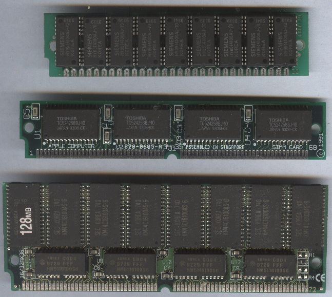
The first variant of SIMMs has 30 pins and provides 8 bits of data (plus a 9th error-detection bit in parity SIMMs). They were used in AT-compatible (286-based, e.g., Wang APC[10]), 386-based, 486-based, Macintosh Plus, Macintosh II, Quadra, Atari STE microcomputers, Wang VS minicomputers and Roland electronic samplers.

The second variant of SIMMs has 72 pins and provides 32 bits of data (36 bits in parity and ECC versions). These appeared first in the early 1990s in later models of the IBM PS/2, and later in systems based on the 486, Pentium, Pentium Pro, early Pentium II, and contemporary/competing chips of other brands. By the mid-90s, 72-pin SIMMs had replaced 30-pin SIMMs in new-build computers, and were starting to themselves be replaced by DIMMs.

Non-IBM PC computers such as UNIX workstations may use proprietary non-standard SIMMs. The Macintosh IIfx uses proprietary non-standard SIMMs with 64 pins.

DRAM technologies used in SIMMs include FPM (Fast Page Mode memory, used in all 30-pin and early 72-pin modules), and the higher-performance EDO DRAM (used in later 72-pin modules).

Due to the differing data bus widths of the memory modules and some processors, sometimes several modules must be installed in identical pairs or in identical groups of four to fill a memory bank. The rule of thumb is a 286, 386SX, 68000 or low-end 68020 / 68030 (e.g. Atari Falcon, Mac LC) system (using a 16 bit wide data bus) would require two 30-pin SIMMs for a memory bank. On 386DX, 486, and full-spec 68020 through 68060 (e.g. Atari TT, Amiga 4000, Mac II) systems (32 bit data bus), either four 30-pin SIMMs or one 72-pin SIMM are required for one memory bank. On Pentium systems (data bus width of 64 bits), two 72-pin SIMMs are required. However, some Pentium systems have support for a "half bank mode", in which the data bus would be shortened to only 32 bits to allow operation of a single SIMM. Conversely, some 386 and 486 systems use what is known as "memory interleaving", which requires twice as many SIMMs and effectively doubles the bandwidth.

The earliest SIMM sockets were conventional push-type sockets. These were soon replaced by ZIF sockets in which the SIMM was inserted at an angle, then tilted into an upright position. To remove one, the two metal or plastic clips at each end must be pulled to the side, then the SIMM must be tilted back and pulled out (low-profile sockets reversed this convention somewhat, like SODIMMs - the modules are inserted at a "high" angle, then pushed down to become more flush with the motherboard). The earlier sockets used plastic retainer clips which were found to break, so steel clips replaced them.

Some SIMMs support presence detect (PD). Connections are made to some of the pins that encode the capacity and speed of the SIMM, so that compatible equipment can detect the properties of the SIMM. PD SIMMs can be used in equipment which does not support PD; the information is ignored. Standard SIMMs can easily be converted to support PD by fitting jumpers, if the SIMMs have solder pads to do so, or by soldering wires on.[11]

30-pin SIMMs

[edit]
30-pin SIMM, 256 KB capacity
Two 30-pin SIMM slots on an IBM PS/2 Model 50 motherboard

Standard sizes: 256 KB, 1 MB, 4 MB, 16 MB.

30-pin SIMMs have 12 address lines, which can provide a total of 24 address bits. With an 8-bit data width, this leads to an absolute maximum capacity of 16 MB for both parity and non-parity modules (the additional redundancy-bit chip usually does not contribute to the usable capacity).

30-pin SIMM
Pin # Name Signal description Pin # Name Signal description
1 VCC +5 VDC 16 DQ4 Data 4
2 /CAS Column address strobe 17 A8 Address 8
3 DQ0 Data 0 18 A9 Address 9
4 A0 Address 0 19 A10 Address 10
5 A1 Address 1 20 DQ5 Data 5
6 DQ1 Data 1 21 /WE Write enable
7 A2 Address 2 22 VSS Ground
8 A3 Address 3 23 DQ6 Data 6
9 VSS Ground 24 A11 Address 11
10 DQ2 Data 2 25 DQ7 Data 7
11 A4 Address 4 26 QP* Data parity out
12 A5 Address 5 27 /RAS Row address strobe
13 DQ3 Data 3 28 /CASP* Parity column address strobe
14 A6 Address 6 29 DP* Data parity in
15 A7 Address 7 30 VCC +5 VDC

* Pins 26, 28 and 29 are not connected on non-parity SIMMs.

72-pin SIMMs

[edit]
72-pin EDO DRAM SIMM

Standard sizes: 1 MB, 2 MB, 4 MB, 8 MB, 16 MB, 32 MB, 64 MB, 128 MB (the standard also defines 3.3 V modules with additional address lines and up to 2 GB)

With 12 address lines, which can provide a total of 24 address bits, two ranks of chips, and 32-bit data output, the absolute maximum capacity is 227 = 128 MB.

5 V 72-pin SIMM
Pin # Name Signal description Pin # Name Signal description
1 VSS Ground 37 MDP1* Data parity 1 (MD8..15)
2 MD0 Data 0 38 MDP3* Data parity 3 (MD24..31)
3 MD16 Data 16 39 VSS Ground
4 MD1 Data 1 40 /CAS0 Column address strobe 0
5 MD17 Data 17 41 /CAS2 Column address strobe 2
6 MD2 Data 2 42 /CAS3 Column address strobe 3
7 MD18 Data 18 43 /CAS1 Column address strobe 1
8 MD3 Data 3 44 /RAS0 Row address strobe 0
9 MD19 Data 19 45 /RAS1 Row address strobe 1
10 VCC +5 VDC 46 NC Not connected
11 NU [PD5#] Not used [presence detect 5 (3v3)] 47 /WE Read/write enable
12 MA0 Address 0 48 NC [/ECC#] Not connected [ECC presence (if grounded) (3v3)]
13 MA1 Address 1 49 MD8 Data 8
14 MA2 Address 2 50 MD24 Data 24
15 MA3 Address 3 51 MD9 Data 9
16 MA4 Address 4 52 MD25 Data 25
17 MA5 Address 5 53 MD10 Data 10
18 MA6 Address 6 54 MD26 Data 26
19 MA10 Address 10 55 MD11 Data 11
20 MD4 Data 4 56 MD27 Data 27
21 MD20 Data 20 57 MD12 Data 12
22 MD5 Data 5 58 MD28 Data 28
23 MD21 Data 21 59 VCC +5 VDC
24 MD6 Data 6 60 MD29 Data 29
25 MD22 Data 22 61 MD13 Data 13
26 MD7 Data 7 62 MD30 Data 30
27 MD23 Data 23 63 MD14 Data 14
28 MA7 Address 7 64 MD31 Data 31
29 MA11 Address 11 65 MD15 Data 15
30 VCC +5 VDC 66 NC [/EDO#] Not connected [EDO presence (if grounded) (3v3)]
31 MA8 Address 8 67 PD1x Presence detect 1
32 MA9 Address 9 68 PD2x Presence detect 2
33 /RAS3 Row address strobe 3 69 PD3x Presence detect 3
34 /RAS2 Row Address Strobe 2 70 PD4x Presence detect 4
35 MDP2* Data parity 2 (MD16..23) 71 NC [PD (ref)#] Not connected [presence detect (ref) (3v3)]
36 MDP0* Data parity 0 (MD0..7) 72 VSS Ground

* Pins 35, 36, 37 and 38 are not connected on non-parity SIMMs.[12]
/RAS1 and /RAS3 are only used on two-rank SIMMS: 2, 8, 32, and 128 MB.
# These lines are only defined on 3.3 V modules.
x Presence-detect signals are detailed in JEDEC standard.

Proprietary SIMMs

[edit]

GVP 64-pin

[edit]

Several CPU cards from Great Valley Products for the Commodore Amiga used special 64-pin SIMMs (32 bits wide, 1, 4 or 16 MB, 60 ns).

Apple 64-pin

[edit]

Dual-ported 64-pin SIMMs were used in Apple Macintosh IIfx computers to allow overlapping read/write cycles (1, 4, 8, 16 MB, 80 ns).[13][14]

5V 64-pin Mac IIfx SIMM[15]
Pin # Name Signal description Pin # Name Signal description
1 GND Ground 33 Q4 Data output bus, bit 4
2 NC Not connected 34 /W4 Write-enable input for RAM IC 4
3 +5V +5 volts 35 A8 Address bus, bit 8
4 +5V +5 volts 36 NC Not connected
5 /CAS Column address strobe 37 A9 Address bus, bit 9
6 D0 Data input bus, bit 0 38 A10 Address bus, bit 10
7 Q0 Data output bus, bit 0 39 A11 Address bus, bit 11
8 /W0 Write-enable input for RAM IC 0 40 D5 Data input bus, bit 5
9 A0 Address bus, bit 0 41 Q5 Data output bus, bit 5
10 NC Not connected 42 /W5 Write-enable input for RAM IC 5
11 A1 Address bus, bit 1 43 NC Not connected
12 D1 Data input bus, bit 1 44 NC Not connected
13 Q1 Data output bus, bit 1 45 GND Ground
14 /W1 Write-enable input for RAM IC 1 46 D6 Data input bus, bit 6
15 A2 Address bus, bit 2 47 Q6 Data output bus, bit 6
16 NC Not connected 48 /W6 Write-enable input for RAM IC 6
17 A3 Address bus, bit 3 49 NC Not connected
18 GND Ground 50 D7 Data input bus, bit 7
19 GND Ground 51 Q7 Data output bus, bit 7
20 D2 Data input bus, bit 2 52 /W7 Write-enable input for RAM IC 7
21 Q2 Data output bus, bit 2 53 /QB Reserved (parity)
22 /W2 Write-enable input for RAM IC 2 54 NC Not connected
23 A4 Address bus, bit 4 55 /RAS Row address strobe
24 NC Not connected 56 NC Not connected
25 A5 Address bus, bit 5 57 NC Not connected
26 D3 Data input bus, bit 3 58 Q Parity-check output
27 Q3 Data output bus, bit 3 59 /WWP Write wrong parity
28 /W3 Write-enable input for RAM IC 3 60 PDCI Parity daisy-chain input
29 A6 Address bus, bit 6 61 +5V +5 volts
30 NC Not connected 62 +5V +5 volts
31 A7 Address bus, bit 7 63 PDCO Parity daisy-chain output
32 D4 Data input bus, bit 4 64 GND Ground

HP LaserJet

[edit]

72-pin SIMMs with non-standard presence detect (PD) connections.

See also

[edit]

References

[edit]
[edit]
Revisions and contributorsEdit on WikipediaRead on Wikipedia
from Grokipedia
A Single In-line Memory Module (SIMM) is a type of (DRAM) module consisting of a small populated with chips and featuring a single row of electrical contacts for plugging into a socket on a computer's to expand available RAM capacity. Developed by and introduced in 1983, SIMMs represented a significant advancement over earlier memory packaging like single in-line pin packages (SIPPs), enabling easier installation and higher densities in personal computers. SIMMs were widely adopted in systems from the late through the , powering processors such as the 286, 386, 486, and early chips, where they provided 32-bit data pathways and typically required installation in pairs to achieve 64-bit bus widths on later architectures. Early variants featured 30 pins and capacities ranging from 256 KB to 16 MB, operating at 5 volts, while later 72-pin models supported up to 128 MB per module, faster access times, and optional parity checking via an additional chip for detection. These modules were non-buffered, meaning they directly interfaced with the without intermediate circuitry, which limited their but made them cost-effective for the era's computing needs. By the late 1990s, SIMMs were largely supplanted by Dual In-line Memory Modules (DIMMs), which offered independent pin connections on both sides, support for 64-bit channels natively, lower voltage requirements (3.3 volts), and greater capacities to meet the demands of evolving processors like the and beyond. Today, SIMMs are obsolete in modern but remain notable in retro , embedded systems, and historical analyses of memory evolution for their role in democratizing RAM upgrades during the personal computer boom.

History

Invention and Early Development

The Single In-line Memory Module (SIMM) was invented in 1983 by James E. Clayton, an engineer at Wang Laboratories, as a compact and cost-effective alternative to discrete dual in-line package (DIP) dynamic random-access memory (DRAM) chips used in personal computers and workstations of the era. The design aimed to simplify memory installation by integrating multiple DRAM chips onto a single removable printed circuit board, enabling higher memory density on motherboards while facilitating user upgrades without soldering. Clayton's innovation addressed the growing demand for expandable memory in computing systems, where traditional discrete chips consumed excessive board space and complicated maintenance. The concept was publicly introduced to the computer industry press by Wang employees, including Clayton, in June 1983, marking an early milestone in modular memory technology. Wang Laboratories was the first to commercialize SIMMs, deploying them in its own professional computer systems shortly after the 1983 invention, with the technology becoming available to external customers by the mid-1980s. The initial SIMM design featured a 30-pin for interfacing with motherboards, supporting up to 256 KB of capacity using fast page mode (FPM) DRAM chips with access times around 100 ns. These modules typically incorporated eight 8-bit DRAM chips arranged in single-sided or double-sided layouts to optimize density, allowing for 256,000 bytes of storage while including provisions for a ninth chip dedicated to parity checking. This configuration provided an eight-fold increase in density compared to conventional discrete DRAM setups, making it suitable for early 1980s systems requiring 64 KB to 1 MB of total RAM. Early development of SIMMs in the faced challenges, particularly the lack of immediate industry standardization, prompting to pursue protection—resulting in U.S. No. 4,656,605 granted in 1987—which led to litigation against competitors like and to enforce the technology's . These hurdles notwithstanding, SIMMs quickly gained traction beyond Wang systems, appearing in early Macintosh computers by the mid- and paving the way for further refinements in modularity.

Adoption and Evolution

The standardization of the 30-pin SIMM in June 1986 facilitated widespread interoperability among vendors, allowing modules from various manufacturers to be used in systems from companies such as and . This standard emerged as personal computers transitioned from socketed DIP memory chips to modular designs, promoting easier upgrades and cost reductions in the late PC market. Key milestones in SIMM adoption included the release of Apple's in March 1987, which featured eight slots for 30-pin SIMMs and marked one of the first major non-IBM systems to integrate them for expandable color graphics and multitasking capabilities. Similarly, IBM's PS/2 line, launched in April 1987, popularized 72-pin SIMMs as a new form factor for higher-density memory in 32-bit architectures, supporting processors like the 386 and 486. The shift to 72-pin SIMMs accelerated around 1990 with the ANSI/EIA-463 standard, which defined their specifications for 32-bit data paths and enabled broader compatibility in desktop and workstation systems. This evolution aligned with the growing demands of 32-bit processors, reducing the need for multiple 30-pin modules per bank from four to one or two. SIMM capacities expanded significantly from 1 MB modules in 1987 to 128 MB by 1996, propelled by advances in DRAM chip densities such as the transition from 4 Mbit devices in 1990 to 64 Mbit chips by the mid-1990s. These density improvements allowed SIMMs to support larger system memories without increasing module size, sustaining their dominance in computing hardware through the early 1990s.

Decline and Obsolescence

The introduction of Dual In-line Memory Modules (s) in 1993 marked the beginning of the decline for Single In-line Memory Modules (SIMMs), as standardized the 72-pin Fast Page Mode (FPM) DIMM to support higher capacities and improved scalability for emerging systems. This transition was accelerated by the adoption of Intel's processors in 1993, which featured a 64-bit external data bus that rendered SIMMs less efficient, requiring multiple modules to be installed in pairs to match the bus width and achieve adequate bandwidth. Processor architecture evolutions beyond the Pentium further emphasized these limitations, as 64-bit bus designs favored DIMMs for seamless integration with error-correcting code (ECC) memory; SIMMs' single-sided or dual-sided configurations with 32-bit or 36-bit (parity) paths necessitated two modules for 72-bit ECC support using 36-bit SIMMs, complicating system design and reducing bandwidth efficiency in server and workstation environments. Market dynamics reflected this shift, with SIMM production reaching its peak around 1996 amid widespread use in 486 and early systems, but major vendors including began phasing out support by 1998 as DIMMs became the standard for new PC architectures. SIMMs persisted in niche applications, such as embedded systems and legacy industrial equipment, through the early , though their overall obsolescence was complete by the mid-2000s in mainstream computing. Economic pressures contributed to the rapid obsolescence, as SIMMs incurred higher manufacturing costs due to the need for gold-plated finger contacts to ensure reliable connectivity in multi-module configurations, alongside limitations in single-bank that hindered compared to the dual-bank design of DIMMs. Proprietary variants, such as those from GVP and Apple, briefly extended SIMM use in specialized platforms like and Macintosh systems into the late 1990s.

Design and Operation

Physical Structure

Single In-line Memory Modules (SIMMs) are constructed as compact printed circuit boards (PCBs) designed for easy insertion into sockets, featuring a single row of electrical contacts along one edge. The module's form factor varies by pin count: 30-pin SIMMs measure approximately 3.5 inches (90 mm) in length and 0.75 inches (19 mm) in height, while 72-pin SIMMs are longer at about 4.25 inches (108 mm) in length and 1 inch (25 mm) in height. These dimensions accommodate the edge connector pins spaced at 0.1-inch (2.54 mm) intervals, ensuring compatibility with standard slots. The PCB serves as the base for mounting (DRAM) chips, typically soldered directly onto one or both sides of the board. Standard configurations include 8 chips for non-parity modules or 9 chips for parity-enabled variants, where the extra chip handles error-checking bits. The edge connector features gold-plated contacts to enhance conductivity and prevent oxidation, promoting long-term reliability in repeated insertions. Optional heat spreaders, often aluminum or plates, could be added to high-density modules to dissipate heat from the DRAM chips during intensive operation. SIMMs support varying density options based on chip arrangement and technology. Single-sided modules, with DRAM chips on one face, typically offer lower capacities such as 1 MB to 4 MB, suitable for basic systems. Double-sided modules, utilizing both PCB surfaces, achieve higher densities up to 32 MB per module by doubling the chip count. For ultra-high-density variants, chip stacking—vertically layering multiple DRAM dies within packages—enabled capacities beyond standard limits, such as 64 MB or more in later 72-pin designs. Installation involves a friction-fit mechanism into dedicated edge sockets on the , angled at 45 degrees for initial insertion before vertical alignment. Modules secure via spring tension in the socket, with no additional clips required in most cases. This supports daisy-chaining configurations in banks, allowing up to 4 modules for 30-pin SIMMs or 8 for extended 72-pin setups to form wider paths, such as 32-bit or 64-bit buses. Over time, pin counts evolved from 30 to 72 to accommodate increasing address and requirements.

Electrical and Signaling Characteristics

Single In-line Memory Modules (SIMMs) initially operated using 5 V TTL logic standards prevalent in the , with supply voltage tolerances of ±10% (4.5 V to 5.5 V) and levels compatible with TTL specifications, such as high-level input voltage (VIH) minimum of 2.4 V and low-level input voltage (VIL) maximum of 0.8 V. This configuration supported early fast page mode (FPM) DRAM operations in systems like the PC/AT and Macintosh. By the , to reduce power requirements and enable denser configurations, SIMMs transitioned to 3.3 V or LVTTL signaling, maintaining compatibility with lower voltage interfaces while adhering to standards that defined distinct power and interface levels for 5 V and 3.3 V modules via physical voltage keys in the sockets to prevent mismatches. Power consumption varied by module type and density, with 30-pin SIMMs typically drawing 3–5 during active operation for configurations up to 8 MB, while standby modes reduced this to approximately 1 or less, as seen in early 1 M × 8 modules at 450 mW active and 6 mW standby. For 72-pin SIMMs, active power reached up to 7 in higher-density units like 32 MB modules (e.g., 1.1 A at 5 V), with standby currents as low as 4–8 mA (around 20–40 mW at 5 V). The 3.3 V variants further lowered consumption, with examples like 2 M × 32 static RAM modules at 2.4 A maximum active (about 8 ) but dropping to 0.5–1 A in standby. Pin assignments followed JEDEC standards, with address lines A0–A11 multiplexed for row and column selection (e.g., A0 on pin 12, A10 on pin 31 for 72-pin). Data lines spanned D0–D31 in 72-pin modules (e.g., D0 on pin 2, D31 on pin 58), supporting 32-bit widths, while 30-pin variants used 8- or 9-bit (with parity) configurations on DQ0–DQ7/DQ8. Control signals included row address strobe (RAS# on pins 44, 34 for multiple banks in 72-pin), column address strobe (CAS# on pins 40–43), and write enable (WE# on pin 47), all active low and TTL-compatible in 5 V designs. Several pins were reserved (e.g., NC on pins 9, 20) for future extensions or presence detect (PD1–PD4 on pins 67–70), which encoded module capacity, speed, and voltage type. Compatibility between voltage standards required careful attention, as 5 V TTL modules could not be safely inserted into 3.3 V slots without level shifters, potentially causing stress on the lower-voltage DRAM chips and leading to burnout or permanent damage. Conversely, 3.3 V modules in 5 V slots often functioned but at reduced performance due to marginal signaling levels, though voltage keys in sockets minimized such errors by physically preventing mismatches.

Memory Access Mechanisms

SIMMs interface with the system bus through standardized protocols that facilitate efficient read and write operations on the underlying DRAM chips. Primarily supporting Fast Page Mode (FPM) DRAM, these modules employ multiplexed address and lines to optimize access. The process begins with the assertion of the row access strobe (RAS) signal, which latches the row address and activates the selected row within the DRAM array. Subsequently, the column access strobe (CAS) signal is asserted to latch the column address, enabling the retrieval or storage of from the specific cell in that row. This RAS-followed-by-CAS allows for burst-mode operations where subsequent column accesses within the same row can occur more rapidly by maintaining RAS active and only cycling CAS, thereby reducing overhead compared to full row activations for each access. Access timings for SIMMs improved over time, starting with early modules rated at approximately 100 ns and progressing to 60 ns in later designs, reflecting advancements in DRAM fabrication. These timings encompass the latency from address assertion to valid data output, with cycle times often exceeding access times due to precharge requirements. To prevent data loss from capacitor leakage, SIMMs require periodic refresh cycles distributed across all rows every 16 ms, commonly achieved via CAS-before-RAS (CBR) refresh. In CBR mode, CAS is asserted first to engage an internal counter, followed by RAS to refresh the addressed row, allowing refreshes to occur transparently during idle bus periods without dedicated cycles. Performance enhancements were realized through bank interleaving, where SIMMs are installed in pairs to create multiple independent banks that can be accessed in a pipelined fashion. This technique overlaps row activations across banks, minimizing wait states and boosting effective bandwidth; for instance, 72-pin SIMMs at 33 MHz bus speeds could achieve higher throughput by alternating accesses between paired modules. Such interleaving is particularly effective for sequential workloads, as one bank precharges while another serves data. For , SIMMs incorporated an optional via a dedicated 9th chip, which computes the even or odd parity of the 8 bits to enable single-bit error detection during reads. If a mismatch occurs, the system can flag the error, though no automatic correction is provided, distinguishing this from more robust error-correcting code (ECC) schemes. This parity mechanism was common in server and environments but absent in non-parity consumer variants.

Standard Configurations

30-pin SIMMs

The 30-pin SIMM represented the initial standardization of single in-line memory modules for (DRAM) in personal computers, emerging in the mid-1980s to support 8-bit and 16-bit architectures. These modules were first widely adopted in systems like the PC XT Model 286 from 1986, which utilized pairs of 30-pin SIMMs to expand beyond base memory configurations of 640 KB. Developed under Standard No. 21-C, the 30-pin design facilitated easier installation compared to earlier discrete DIP chips, enabling memory upgrades in low-end workstations, entry-level servers, and compatible PCs. These modules operated with an 8-bit data width in non-parity configurations or 9-bit when including a for error detection, aligning with the bus widths of contemporary 8-bit systems like the PC/XT or 16-bit setups requiring paired modules. Early capacities started at 256 KB using 256 kbit DRAM chips but scaled to a maximum of 16 MB per module with 16 Mbit DRAM integration, limited by the 12 multiplexed address lines that supported up to 24 address bits total. Access speeds varied from 120 ns in initial implementations to 80 ns in later variants, balancing cost and performance for applications in basic computing tasks and light server duties. A key limitation of the 30-pin SIMM was its single-bank , which constrained interleaving and thus hindered efficient multitasking by preventing parallel access across multiple banks during high-demand operations. For 16-bit operation in systems like early 286 machines, modules had to be installed in pairs within even-numbered slots to form a complete 16-bit bank, often resulting in underutilized odd slots if not fully populated and complicating expansion. This design, while reliable for , became a bottleneck as processor speeds increased, paving the way for wider variants.

72-pin SIMMs

The 72-pin SIMM represented a significant from the earlier 30-pin design, optimized for 32-bit data paths to support processors like the 80386, 80486, and initial series. Standardized by in 1990 under publication 21-C for DRAM module families, it enabled single-module installation to fill a full 32-bit (or 36-bit with parity) bank, simplifying expansion compared to requiring multiple 30-pin modules. Major vendors such as AST Research and Micron Technology produced these modules, which became ubiquitous in 386, 486, and Pentium-based PCs throughout the early 1990s. Available in capacities from 4 MB to 256 MB, they accommodated growing system requirements while supporting both Fast Page Mode (FPM) and Extended Data Out (EDO) DRAM types. EDO variants provided enhanced page-mode access efficiency, achieving up to 20% faster performance than FPM in non-cached operations by extending data output timing. A defining feature was the presence detect pins (PD0-PD2), which encoded the module's capacity and access speed—such as 60 ns or 70 ns—allowing systems to automatically configure memory without manual intervention. Optional burst mode capability further improved efficiency for cache line fills, leveraging pipelined accesses in compatible controllers like those for the 80486. Variants differed in contact plating, with gold-fingered modules offering superior corrosion resistance for long-term reliability when matched to gold sockets, while tin contacts were more cost-effective but prone to oxidation if mismatched. Additionally, 3.3 V low-voltage versions emerged for power-sensitive applications, including early PowerPC Macintosh systems, incorporating keyed pin definitions to prevent incorrect insertion and ensure reduced power draw while maintaining compatibility with JEDEC signaling.

Proprietary Variants

GVP 64-pin SIMM

The GVP 64-pin SIMM was developed by Great Valley Products (GVP) in 1989 specifically for their Impact A3001 accelerator card, targeted at the and subsequent models like the . This proprietary addressed the limitations of standard Amiga memory expansion by providing a custom interface for Fast RAM in accelerator environments, where the original architecture restricted total Fast RAM to 8 MB via trapdoor expansions. The design bridged the need for 32-bit data paths in high-performance setups, utilizing a non-standard pinout incompatible with norms to optimize integration with GVP's hardware. These SIMMs supported capacities of 1 MB, 4 MB, and up to 16 MB per module, populated with page-mode DRAM chips operating at 60 ns access speeds for compatibility with 33–50 MHz processor clocks. Configurations varied by accelerator model; for instance, the Impact A3001 featured eight sockets for up to 20 MB total using 1 MB or 4 MB modules, while later G-Force 040 cards used four sockets to achieve 64 MB total with 16 MB modules. The modules required matching speeds and sizes within a board to enable features like burst mode access, ensuring reliable performance in 32-bit addressing spaces. Compatible exclusively with GVP accelerator and combo boards—such as the Impact series, G-Force series, and A530 accelerator—these SIMMs featured keyed notches to prevent incorrect insertion and jumper-configurable settings on the host cards for memory mapping. This exclusivity stemmed from the custom electrical characteristics tailored to GVP's DMA-capable controllers and CPU slots, preventing use in non-GVP expansions or other platforms. Installation often necessitated updates or patches to recognize expanded memory beyond 8 MB, along with hardware jumpers for optimal signal handling and autoconfiguration. The GVP 64-pin SIMM significantly impacted users by enabling memory expansions that supported demanding applications like and multitasking, far surpassing the base system's capabilities during the late and early . For example, a fully populated Impact A3001 could deliver 20 MB of 32-bit Fast RAM, facilitating smoother operation under 68030 processors. However, the nature limited availability and interchangeability, contributing to higher costs and dependence on GVP's ecosystem until the company's decline in the mid-1990s.

Apple 64-pin SIMM

The Apple 64-pin SIMM was a proprietary memory module introduced in 1990 with the Macintosh IIfx, designed to support 32-bit clean addressing in Apple's 68030-based systems through its 64 pins, which incorporated extended control lines for enhanced signaling beyond the standard 30-pin SIMM configuration. This design enabled full 32-bit data paths and addressed the limitations of earlier 24-bit addressing modes in Macintosh hardware, allowing access to up to 4 GB of theoretical address space. The module's architecture was tailored for high-performance operation in the IIfx, featuring dual-ported access to reduce latency in memory reads and writes. Available in capacities of 1 MB, 4 MB, and 16 MB per module, the Apple 64-pin SIMM supported configurations from 4 MB to 128 MB total when installed in groups of four across the IIfx's eight slots, optimized for the 40 MHz 68030 processor at 80 ns access speeds. These SIMMs included parity bits for error detection, with the system's capable of parity errors to aid in diagnostics and maintenance. The design emphasized reliability for professional desktop use, though maximum expansion required matching modules in each bank to maintain compatibility and performance. Key design quirks included non-standard pin spacing and a 5V-only voltage requirement, making the SIMMs incompatible with third-party expansion boards or other Macintosh models without custom adapters or socket modifications. This proprietary form factor, distinct from standards, ensured tight integration with Apple's hardware but limited aftermarket options and contributed to higher costs for upgrades. Primarily deployed in the desktop until its discontinuation in 1992, the Apple 64-pin SIMM saw continued use in legacy 68k-based systems through the mid-1990s, ultimately phased out with Apple's transition to PowerPC processors and 72-pin SIMM architectures in 1994.

HP LaserJet SIMM

HP SIMMs were introduced with later models in the series, starting with 30-pin variants in the LaserJet III (1990) and transitioning to 72-pin in the (1993), with capacities ranging from 1 MB to 16 MB (and up to 32 MB in mid-1990s models) specifically for expanding RAM to store scalable and bitmap fonts, page buffers, and bitmap images to enhance printing capabilities. These modules built upon standard SIMM physical structures but incorporated adaptations for printer environments, such as operating at 5 V with support for flash ROM to allow non-volatile storage of custom fonts and forms. They utilized standard pinouts but featured printer-specific configurations, including serial ID via grounded or open circuits on pins like 67-70 to encode module size, speed, and type, enabling automatic recognition and configuration by the printer in later models (e.g., LaserJet 5 series). This facilitated seamless integration of emulation via dedicated personality SIMMs, expanding compatibility for advanced graphics and font rendering without software reconfiguration. In practice, SIMMs served a specialized niche by allowing incremental upgrades to prolong the operational lifespan of LaserJet printers, particularly for high-volume font caching and page buffering in environments. Production and support for these modules ceased around 2000, supplanted by onboard integration and the shift to architectures in subsequent LaserJet models for improved scalability and ease of installation.

Legacy and Comparisons

Transition to DIMMs

The standardization of the 168-pin DIMM by JEDEC in the mid-1990s introduced a form factor that supported independent memory banks on each side of the module, enabling direct implementation of error-correcting code (ECC) without the interleaving required for SIMMs to achieve equivalent bus widths. This design shift addressed limitations in SIMM architectures, where modules had to be installed in pairs to form a 64-bit channel, complicating ECC configurations and increasing signal integrity challenges. Compatibility between SIMMs and DIMMs proved challenging, as the differing pin counts, voltage requirements (typically 5V for SIMMs versus 3.3V for most s), and signaling protocols prevented direct interchangeability. Adapters from SIMM to DIMM slots were rare, often inefficient due to added latency and potential instability, and largely impractical for widespread adoption. By , the introduction of Intel's processor necessitated full motherboard redesigns to accommodate DIMM slots exclusively, accelerating the shift away from SIMM-based systems. SIMMs maintained dominance in the personal computer market through the mid-1990s, but by 1998, DIMMs had largely supplanted them in mainstream consumer and applications due to superior and . Holdouts persisted in budget-oriented systems into the early , where cost constraints favored legacy SIMM compatibility, while embedded systems and legacy industrial applications continued using SIMMs into the early . A key driver of the transition was economic: DIMMs proved cheaper to manufacture and assemble at scale, as a single module could deliver 64-bit operation without the paired installation and additional traces required for SIMMs, streamlining production and reducing system costs. This manufacturing efficiency, combined with declining SIMM production volumes, further eroded the economic viability of SIMMs by the late .

Advantages and Limitations

SIMMs offered several advantages that made them a practical choice for memory expansion in early personal computers and workstations during the 1980s and 1990s. Their modular design allowed for straightforward upgrades without , enabling users to increase system capacity by simply inserting additional modules into available slots, which was a significant improvement over earlier soldered or socketed DIP packages. This ease of installation contributed to their widespread adoption, as they required no specialized tools and minimized the risk of damaging pins or sockets compared to pin-based predecessors. Additionally, SIMMs were compact, occupying minimal space on motherboards, which was particularly beneficial for space-constrained systems like early Macintosh or models. In terms of cost-effectiveness, SIMMs provided an affordable path to boosting memory, with prices reflecting the era's economics; for instance, an 8 MB module could be acquired for approximately $200 in 1992, allowing upgrades that extended the life of aging hardware without full system replacement. Despite these benefits, SIMMs had notable limitations that constrained their performance and longevity. Their asynchronous operation capped effective bandwidth, with 72-pin variants typically achieving around 100–200 MB/s in practical 32-bit bus configurations at bus speeds up to 66 MHz, though real-world throughput was often lower due to latency in Fast Page Mode or EDO DRAM implementations. SIMMs lacked native support for synchronous DRAM (SDRAM), which synchronizes memory access with the system clock for higher efficiency; this incompatibility limited their use in evolving architectures, as SDRAM required the transition to DIMM form factors with independent signaling. Furthermore, in multi-module banks, SIMMs were prone to signal skew and loading issues, as all modules shared common address and control lines, leading to timing mismatches and reduced reliability when populating full banks with mismatched speeds or capacities. Compared to contemporaries, SIMMs were simpler and more user-friendly than Single In-line Pin Packages (SIPPs), which featured protruding pins on one side that were susceptible to bending during insertion, whereas SIMMs used edge connectors for secure, damage-resistant seating. However, they were less scalable for high-speed applications than Inline Memory Modules (RIMMs), which supported faster clocked interfaces but demanded precise termination and were more complex to implement. In modern retro computing, SIMMs hold collectible value for enthusiasts restoring vintage systems like 386/486 PCs or workstations, often fetching $20–$50 per module on secondary markets as of 2025 due to their scarcity and compatibility with period hardware. However, modules over 30 years old carry risks from capacitor degradation, including leakage from electrolytic decoupling capacitors that can cause or short circuits if not inspected or recapped.

References

Add your contribution
Related Hubs
Contribute something
User Avatar
No comments yet.