Recent from talks
Nothing was collected or created yet.
TO-126
View on Wikipedia
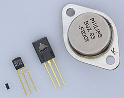
TO-126 is a type of semiconductor package for devices with three pins, such as transistors.[1] The package is rectangular with a hole in the middle to allow for easy mounting to a board or a heat sink. On one side of the package typically a metal sheet is exposed, with the transistor die bonded to the other side of the metal sheet inside the package.[2] This allows for an efficient heat transfer from the transistor die to an external heat sink but also implies that the metal sheet is electrically connected to the die (for a bipolar junction transistor usually the collector is connected to this metal sheet).
History and origin
[edit]The JEDEC TO-126 descriptor is derived from the original full name for the package: Transistor Outline Package, Case Style 126.[3] In the updated JEDEC outline system, the package is numbered as TO-225AA.[2]
STMicroelectronics refers to this package style as SOT-32.[4]
National Standards
[edit]
| Standards organization | Standard | Designation for TO-126 |
|---|---|---|
| JEDEC | JEP95[5] | TO-225AA |
| IEC | IEC 60191[6] | A56 |
| DIN | DIN 41869[7] | 12A3 |
| Gosstandart | GOST 18472—88[8] | KT-27[a] |
| Rosstandart | GOST R 57439—2017[9] | |
| Kombinat Mikroelektronik Erfurt | TGL 11811[6] | N |
| TGL 26713/09[6] | H1B |
See also
[edit]References
[edit]- ^ BD135; BD137; BD139; NPN power transistors (PDF), Philips Semiconductors, 1999, retrieved 2013-12-09
- ^ a b Bill Roehr (2001), AN1040/D: Mounting Considerations For Power Semiconductors (PDF), On Semiconductor, retrieved 2014-01-25
- ^ "JEDEC TO-126 package specification" (PDF). JEDEC. May 1968. Archived from the original (PDF) on June 18, 2017.
- ^ MJE340 MJE350 Complementary silicon power transistors (PDF), STMicroelectronics
- ^ "TO-225" (PDF). JEDEC. Archived from the original (PDF) on 2016-04-10. Retrieved 2021-06-21.
- ^ a b c "TGL 26713/09: Gehäuse für Halbleiterbauelemente - Bauform H" [Outline drawings for semiconductor devices; Type H] (PDF) (in German). Leipzig: Verlag für Standardisierung. June 1988. Retrieved 2021-06-15.
- ^ "NPN Silicon Transistors BD135 BD137 BD139" (PDF). Siemens. Retrieved 2021-08-20.
- ^ "ГОСТ 18472—88 ПРИБОРЫ ПОЛУПРОВОДНИКОВЫЕ - Основные размеры" [GOST 18472—88 Semiconductor devices - basic dimensions] (PDF) (in Russian). Rosstandart. 1988. p. 56. Retrieved 2021-06-17.
- ^ "ГОСТ Р 57439—2017 ПРИБОРЫ ПОЛУПРОВОДНИКОВЫЕ - Основные размеры" [GOST R 57439—2017 Semiconductor devices - basic dimensions] (PDF) (in Russian). Gosstandart. 2017. p. 70-71. Retrieved 2021-06-17.
External links
[edit]- TO-126 Package, EESemi.com

