

Xenon (processor)
View on Wikipedia
 Picture of the microprocessor (XCPU-ES shown) | |
| General information | |
|---|---|
| Designed by | IBM |
| Common manufacturer | |
| Physical specifications | |
| Cores |
|
| Cache | |
| L1 cache | 32/32 KB |
| L2 cache | 1 MB |
| Architecture and classification | |
| Instruction set | PowerPC |
| POWER, PowerPC, and Power ISA architectures |
|---|
| NXP (formerly Freescale and Motorola) |
| IBM |
|
| IBM/Nintendo |
| Other |
| Related links |
| Italics = discontinued • Gray = cancelled |
Microsoft XCPU, codenamed Xenon, is a CPU used in the Xbox 360 game console, to be used with ATI's Xenos graphics chip.
The processor was developed by Microsoft and IBM under the IBM chip program codenamed "Waternoose", which was named after the Monsters, Inc. character Henry J. Waternoose III.[1] The development program was originally announced on November 3, 2003.[2]
The processor is based on IBM PowerPC instruction set architecture. It consists of three independent processor cores on a single die. These cores are slightly modified versions of the PPE in the Cell processor used on the PlayStation 3.[3][4] Each core has two symmetric hardware threads (SMT), for a total of six hardware threads available to games. Each individual core also includes 32 KB of L1 instruction cache and 32 KB of L1 data cache.
The XCPU processors were manufactured at IBM's East Fishkill, New York fabrication plant and Chartered Semiconductor Manufacturing (now part of GlobalFoundries) in Singapore.[5] Chartered reduced the fabrication process in 2007 to 65 nm from 90 nm, thus reducing manufacturing costs for Microsoft.
Specifications
[edit]- 90 nm process,[6] 65 nm process upgrade in 2007[7] (codenamed "Loki"), 45 nm process since Xbox 360 S model,[8] 32 nm process since Xbox 360 E Winchester Motherboard. [citation needed]
- 165 million transistors
- Three cores, each two-way SMT-capable and clocked at 3.2 GHz[6]
- SIMD: Two VMX128 units with a dedicated (128×128 bit) register file for each core,[6] one for each thread
- 1 MB L2 cache[6] (lockable by the GPU) running at half-speed (1.6 GHz) with a 256-bit bus
- 51.2 GB/s of L2 memory bandwidth (256 bit × 1600 MHz)
- 21.6 GB/s front-side bus (On the CPU side, this interfaces to a 1.35 GHz, 8B wide, FSB dataflow; on the GPU side, it connects to a 16B wide FSB dataflow running at 675 MHz.)[6]
- Dot product performance: 9.6 billion per second
- In-order instruction execution[6]
- 768 bits of IBM eFUSE-based OTP memory[9]
- ROM (and 64 KB SRAM) storing Microsoft's Secure Bootloader, and encryption hypervisor[9]
- Big-endian architecture
XCGPU
[edit]The Xbox 360 S introduced the XCGPU (codename Vejle), which integrated the Xenon CPU and the Xenos GPU onto the same die, and the eDRAM into the same package. The XCGPU follows the trend started with the integrated EE+GS in PlayStation 2 Slimline, combining CPU, GPU, memory controllers and IO in a single cost-reduced chip. It also contains a "front side bus replacement block" that connects the CPU and GPU internally in exactly the same manner as the front side bus would have done when the CPU and GPU were separate chips, so that the XCGPU doesn't change the hardware characteristics of the Xbox 360.
XCGPU contains 372 million transistors and is manufactured by GlobalFoundries on a 45 nm process. Compared to the original chipset in the Xbox 360 the combined power requirements are reduced by 60% and the physical chip area by 50%.[10][11]
In 2014, the Winchester Xbox 360 system introduced a shrunken XCGPU on a 32 nm process (codename Oban). This chip is no longer a multi-chip-module and integrates the eDRAM into the main die.
Gallery
[edit]Illustrations of the different generations of processors in Xbox 360 and Xbox 360 S.
-
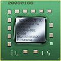 The original XCPU DD2 ES manufactured at 90 nm by IBM in 2005. ES stands for "Engineering Sample" and the device is packaged by IBM at their Bromont facility in Canada. It runs at 2.8GHz, as opposed to the final chip, which ran at 3.2GHz.
 -
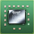 The 90nm XCPU DD3 manufactured at 90 nm by Chartered in Singapore 2006
 -
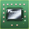 The 65nm XCPU "Loki" manufactured at 65 nm by Chartered in Singapore 2007
 -
 The two chips of the XCGPU "Vejle": The larger is the XCGPU itself and the smaller is the 10 MB eDRAM. Manufactured at 45 nm by Global Foundries in Singapore in 2010.
 -
 The XCGPU with heatspreader. The complete device is packaged by IBM at their Bromont facility in Canada.


References
[edit]- ^ Takahashi, Dean (May 1, 2006). "Learning from failure - The inside story on how IBM out-foxed Intel with the Xbox 360". Electronic Business. Archived from the original on August 27, 2009.
- ^ "IBM News room - 2003-11-03 Microsoft and IBM Announce Technology Agreement - United States". ibm.com. Archived from the original on October 12, 2007.
- ^ "Processing The Truth: An Interview With David Shippy", Leigh Alexander, Gamasutra, January 16, 2009
- ^ "Playing the Fool", Jonathan V. Last, Wall Street Journal, December 30, 2008
- ^ "IBM News room - 2005-10-25 IBM Delivers Power-based Chip for Microsoft Xbox 360 Worldwide Launch - United States". ibm.com. Archived from the original on May 14, 2006.
- ^ a b c d e f Jeffrey Brown (December 6, 2005). "Application-customized CPU design: The Microsoft Xbox 360 CPU story". IBM. Archived from the original on October 25, 2007. Retrieved September 8, 2007.
- ^ César A. Berardini (August 21, 2006). "Chartered to Manufacture 65-nm Xbox 360 CPUs". Archived from the original on January 23, 2008. Retrieved January 9, 2008.
- ^ Patel, Nilay (June 14, 2010). "New Xbox 360 looks angular and Ominous". Engadget.com. Retrieved June 14, 2010.
- ^ a b "Xbox360 security system". YouTube. Archived from the original on December 19, 2021.
- ^ Jon Stokes, Ars Technica (August 24, 2010). "Microsoft beats Intel, AMD to market with CPU/GPU combo chip". Retrieved August 24, 2010.
- ^ PC Perspective (June 21, 2010). "The New Xbox 360 S "Slim" Teardown: Opened and Tested". Archived from the original on June 25, 2010. Retrieved June 24, 2010.
- Xenon hardware overview Archived February 20, 2006, at the Wayback Machine by Pete Isensee, Development Lead, Xbox Advanced Technology Group, written some time before June 23, 2007
External links
[edit]| Hardware | |
|---|---|
| Accessories | |
| System software | |
| Xbox Live | |
| Games | |
| Related | |

Xenon (processor)
View on GrokipediaHistory and development
Design origins
The development of the Xenon processor stemmed from a strategic collaboration between Microsoft and IBM, which began in 2002 as Microsoft initiated planning for the successor to its original Xbox console. Microsoft selected IBM to design a custom central processing unit optimized for high-performance gaming, leveraging IBM's expertise in PowerPC architectures. This partnership resulted in a tailored processor that diverged from standard commercial designs to meet the unique requirements of console hardware.[5] Xenon drew its technical foundations from IBM's Power Processing Element (PPE), originally developed as part of the Cell processor architecture for heterogeneous computing. Unlike the Cell, which combined one PPE with multiple specialized Synergistic Processing Elements (SPEs) for vector-heavy tasks, Xenon featured three identical symmetric PPE cores to enable balanced, general-purpose processing. This customization prioritized scalability within a constrained die area while maintaining compatibility with the PowerPC instruction set architecture.[6][3] The core design philosophy of Xenon focused on exploiting thread-level parallelism (TLP) to address the irregular, multi-threaded nature of gaming workloads, where developers could distribute tasks across cores for improved throughput. To achieve this efficiently, each core adopted an in-order execution model, eschewing the power-hungry out-of-order execution pipelines found in contemporary desktop processors; this approach significantly reduced complexity, die size, and power draw without sacrificing the parallelism essential for real-time rendering and simulation.[6][3] A key aspect of Xenon's design was the deliberate exclusion of SPEs, which were integral to the Cell's high-performance vector processing but introduced significant programming challenges due to their heterogeneous nature and limited instruction sets. By committing to symmetric PPE cores, Microsoft and IBM simplified the development model for game programmers, allowing standard multi-threading techniques without the need to manage specialized coprocessors or data transfers between dissimilar units. This uniform architecture facilitated faster porting of software and broader tool support, aligning with the goal of accessible high-performance computing in a consumer console.[3]Announcement and production
The Xenon processor was officially announced on November 3, 2003, as part of a technology licensing agreement between Microsoft and IBM for semiconductor processors to power future Xbox products.[7][8] Manufacturing of the Xenon processor was handled primarily by IBM, with additional production outsourced to Chartered Semiconductor Manufacturing in Singapore under license from IBM and Microsoft.[9] Initial production ramped up during 2004 and 2005 to meet demand for the upcoming console launch. The processor debuted with the Xbox 360's worldwide rollout, beginning in North America on November 22, 2005, followed by Europe on December 2 and Japan on December 10.[10] By the end of its lifecycle, over 80 million Xbox 360 units incorporating the Xenon processor had been produced and sold globally.[11]Architecture
Processor cores
The Xenon processor incorporates three identical PowerPC Processing Elements (PPEs), each configured as a 64-bit, two-way superscalar, in-order core derived from the design used in IBM's Cell processor.[6][12] These cores handle general-purpose scalar computations, emphasizing efficient throughput for gaming workloads through their balanced architecture. Each PPE supports simultaneous multithreading (SMT) with two hardware threads, enabling the processor to manage up to six concurrent threads overall and improving utilization of the execution resources under varying loads.[6] The execution model relies on in-order instruction dispatch, which simplifies the design and power consumption while prioritizing predictable performance in real-time environments. The pipeline in each core spans 21 stages, facilitating high clock speeds but requiring careful software management to mitigate latency from mispredicted branches, which use static prediction mechanisms without dynamic out-of-order reordering.[6] This deep pipeline structure supports the core's focus on sustained instruction throughput rather than speculative complexity. For arithmetic operations, each core includes an integer arithmetic logic unit (ALU), a scalar floating-point unit (FPU) optimized for 64-bit precision, a branch unit, and a load/store unit, enabling paired execution of scalar instructions per cycle when possible within the two-way superscalar framework.[3][13]Vector processing and extensions
The Xenon processor incorporates a VMX-128 vector media extension unit in each of its three cores, providing dedicated hardware acceleration for multimedia and graphics workloads.[13] This unit supports 4-way single instruction, multiple data (SIMD) operations across floating-point, permute, and simple execution pipelines, enabling efficient processing of 128-bit (16-byte) vectors for integer, floating-point, and packed data types.[13] Each core features a duplicated register file for its dual-threaded execution model, yielding 128 128-bit vector registers per thread and 256 total per core, which allows independent vector operations for concurrent threads without context switching overhead.[6] Xenon's VMX-128 implementation includes specialized load and store instructions optimized for Direct3D compressed data formats, facilitating rapid decompression and manipulation of texture and vertex data in gaming applications.[13] It also supports paired singles floating-point operations through its 4-way SIMD capabilities, allowing simultaneous computation on two 64-bit pairs within a 128-bit register for tasks like 3D transformations.[13] Custom extensions to the underlying PowerPC instruction set further enhance performance, including a dedicated single-cycle dot-product instruction for vector mathematics in graphics and physics simulations, as well as branch hints to optimize prediction in branch-heavy code sequences common in game logic and AI.[6][13] Unlike the full AltiVec vector extension in standard PowerPC processors, Xenon's VMX-128 is a tailored subset focused on gaming efficiency, omitting certain general-purpose features in favor of graphics-specific enhancements like the D3D format support and custom dot-product, which streamline 3D rendering and simulation workloads.[13] This design enables the processor to handle parallel vector tasks effectively within its in-order execution pipeline, contributing to the Xbox 360's capabilities in real-time graphics and physics processing.[6]Cache and memory subsystem
The Xenon processor utilizes a Harvard architecture for its primary caches, with each of the three cores equipped with a dedicated 32 KB L1 instruction cache and a 32 KB L1 data cache, the instruction cache implemented as a 2-way set-associative structure and the data cache as a 4-way set-associative structure to balance hit rates and complexity in a multithreaded environment.[6][13] These L1 caches provide fast, private access for core-specific operations, minimizing latency for frequently used instructions and data while supporting the processor's symmetric multithreading model.[14] A shared 1 MB unified L2 cache serves all three cores, configured as 8-way set-associative with 128-byte cache lines to promote efficient data reuse across threads and reduce contention in bandwidth-limited scenarios.[14][13] This L2 cache incorporates software-controlled prefetching mechanisms, allowing developers to issue hints for anticipating data needs and mitigating stalls in streaming-heavy workloads typical of gaming applications.[6] The memory subsystem interfaces with 512 MB of GDDR3 RAM through a 128-bit wide front-side bus clocked at 711 MHz, achieving a peak bandwidth of 22.4 GB/s to support high-throughput demands from both CPU and integrated graphics processing.[2] This unified memory design enables seamless sharing between the Xenon CPU and the Xenos GPU, eliminating the need for dedicated video memory pools and optimizing overall system resource utilization.[2] Direct memory access (DMA) capabilities allow the GPU to perform efficient transfers to and from main memory without CPU intervention, enhancing performance for graphics-intensive tasks.[14] Cache coherency in this shared environment is managed via software protocols, requiring explicit invalidations and flushes to synchronize CPU cache states with GPU modifications and prevent data inconsistencies.[6]Specifications
Core parameters
The original Xenon processor features three symmetric cores, each operating at a clock speed of 3.2 GHz, providing a total theoretical throughput of 9.6 GHz across the multi-core design.[2] The CPU incorporates approximately 165 million transistors on its original die, fabricated using IBM's 90 nm SOI process technology.[14] Power consumption for the CPU package is rated at a thermal design power (TDP) of 75-85 W, reflecting the high-performance demands of the triple-core configuration in the console environment.[15] The die measures 168 mm², balancing performance density with manufacturing constraints at the 90 nm node. These parameters support the cores' superscalar architecture and simultaneous multithreading capabilities, allowing efficient handling of dual threads per core without delving into detailed functional implementation.[6]| Parameter | Value |
|---|---|
| Clock Speed | 3.2 GHz (per core, all three cores) |
| Transistor Count | 165 million |
| TDP | 75-85 W |
| Die Size | 168 mm² (90 nm process) |