
Community hub
Recent from talks
Contribute something
Nothing was collected or created yet.
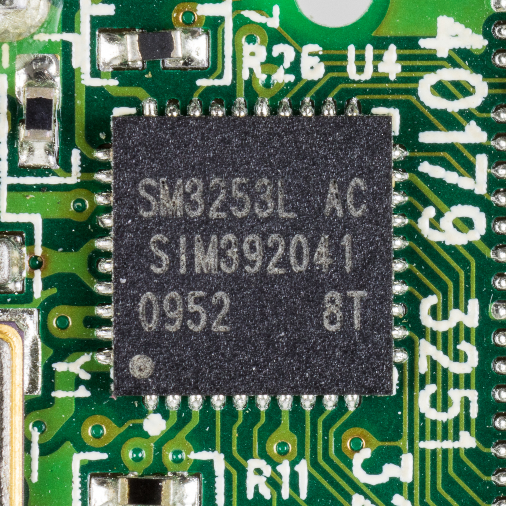
Flash memory controller
View on Wikipedia
A flash memory controller (or flash controller) manages data stored on flash memory (usually NAND flash) and communicates with a computer or electronic device. Flash memory controllers can be designed for operating in low duty-cycle environments like memory cards, or other similar media for use in PDAs, mobile phones, etc. USB flash drives use flash memory controllers designed to communicate with personal computers through the USB port at a low duty-cycle. Flash controllers can also be designed for higher duty-cycle environments like solid-state drives (SSDs) used as data storage for laptop computer systems up to mission-critical enterprise storage arrays.[1]
Initial setup
[edit]After a flash storage device is initially manufactured, the flash controller is first used to format the flash memory. This ensures the device is operating properly, it maps out bad flash memory cells, and it allocates spare cells to be substituted for future failed cells. Some part of the spare cells is also used to hold the firmware which operates the controller and other special features for a particular storage device. A directory structure is created to allow the controller to convert requests for logical sectors into the physical locations on the actual flash memory chips.[1]
Reading, writing, and erasing
[edit]When the system or device needs to read data from or write data to the flash memory, it will communicate with the flash memory controller. Simpler devices like SD cards and USB flash drives typically have a small number of flash memory die connected simultaneously. Operations are limited to the speed of the individual flash memory die. In contrast, a high-performance solid-state drive will have more dies organized with parallel communication paths to enable speeds many times greater than that of a single flash die.[citation needed]
Wear-leveling and block picking
[edit]Flash memory can withstand a limited number of program-erase cycles. If a particular flash memory block were programmed and erased repeatedly without writing to any other blocks, the one block would wear out before all the other blocks thereby prematurely ending the life of the storage device. For this reason flash controllers use a technique called wear leveling to distribute writes as evenly as possible across all the flash blocks in the SSD. In a perfect scenario this would enable every block to reach its terabytes written threshold.[2]
Flash translation layer (FTL) and mapping
[edit]Usually, flash memory controllers also include the "flash translation layer" (FTL), a layer below the file system that maps host side or file system logical block addresses (LBAs) to the physical address of the flash memory (logical-to-physical mapping). The LBAs refer to sector numbers and to a mapping unit of 512 bytes. All LBAs that represent the logical size visible to and managed by the file system are mapped to a physical location (block ID, page ID and sector ID) of the flash memory. As part of the wear leveling and other flash management algorithms (bad block management, read disturb management, safe flash handling etc.), the physical location of an LBA might dynamically change frequently. The mapping units of an FTL can differ so that LBAs are mapped block-, page- or even sub-page-based. Depending on the usage pattern, a finer mapping granularity can significantly reduce the flash wear out and maximize the endurance of a flash based storage media.[3][4][5] The deduplication function to eliminate redundant data and duplicate writes is also added in FTL.[6]
As the FTL metadata takes up its own flash space, it needs protection in case of power loss. In addition, it is possible for the mapping table to wear out before other parts of the flash memory has, prematurely ending the life of a storage device. This is usually avoided in enterprise devices by allocating an oversized space for spares, although more durable forms of storage like MRAM has been proposed for FTL too.[citation needed]
The FTL may have three types: page mapping, block mapping, and hybrid mapping. Page mapping can have higher performance, but it has bigger FTL metadata size and higher cost, and is usually used on solid state drives. Block mapping can have smaller metadata size and lower cost, but it has lower performance, and is usually used on USB flash drives. On page mapping FTL implementations, the ratio of FTL metadata size and storage capacity is usually 1:1000, for example, a 1TB flash storage device may have 1GB of FTL metadata.
Garbage collection
[edit]Once every block of a solid-state storage device has been written one time, the flash controller will need to return to some of the initial blocks which no longer have current data (also called stale blocks). The data in these blocks were replaced with newly written blocks and now they are waiting to be erased so that new data can be written into them. This is a process called garbage collection (GC). All SSDs, CF cards and other flash storage devices will include some level of garbage collection. The speed at which a flash controller will do this can vary.[7]
References
[edit]- ^ a b "Flash Memory Guide" (PDF). kingston.com. Retrieved 7 March 2013.
- ^ Chang, Li-Pin (2007-03-11). "On Efficient Wear Leveling for Large Scale Flash Memory Storage Systems". CiteSeerX 10.1.1.103.4903.
- ^ Goodson, Garth; Iyer, Rahul. "Design Tradeoffs in a Flash Translation Layer" (PDF). Archived from the original (PDF) on June 23, 2015.
- ^ "Understanding Flash: The Flash Translation Layer". September 17, 2014.
- ^ Heidrich, Susan (February 2015). "New flash management architecture enables MLC for industrial storage" (PDF). Archived from the original (PDF) on 2015-06-23. Retrieved 2015-06-23.
- ^ Chen, Feng; Luo, Tian; Zhang, Xiaodong (2011). CAFTL: a content-aware flash translation layer enhancing the lifespan of flash memory based solid state drives. FAST' 11. p. 6.
- ^ "SSDs - Write Amplification, TRIM and GC" (PDF). OCZ Technology. Archived from the original (PDF) on 2012-05-26. Retrieved 2010-05-31.
| Key terminology | |||||
|---|---|---|---|---|---|
| Flash manufacturers | |||||
| Controllers |
| ||||
| SSD manufacturers | |||||
| Interfaces |
| ||||
| Configurations | |||||
| Related organizations | |||||