



Community hub
Wikipedia
LGA 1151
View on Wikipedia
 | |
| Release date | September 1, 2015 |
|---|---|
| Designed by | Intel |
| Manufactured by | Lotes |
| Type | LGA-ZIF |
| Chip form factors | Flip-chip |
| Contacts | 1151 |
| FSB protocol | PCI Express |
| Processor dimensions | 37.5 × 37.5 mm 1,406.25 mm²[1] |
| Processors | |
| Predecessor | LGA 1150 |
| Successor | LGA 1200 |
| Memory support | |
This article is part of the CPU socket series | |
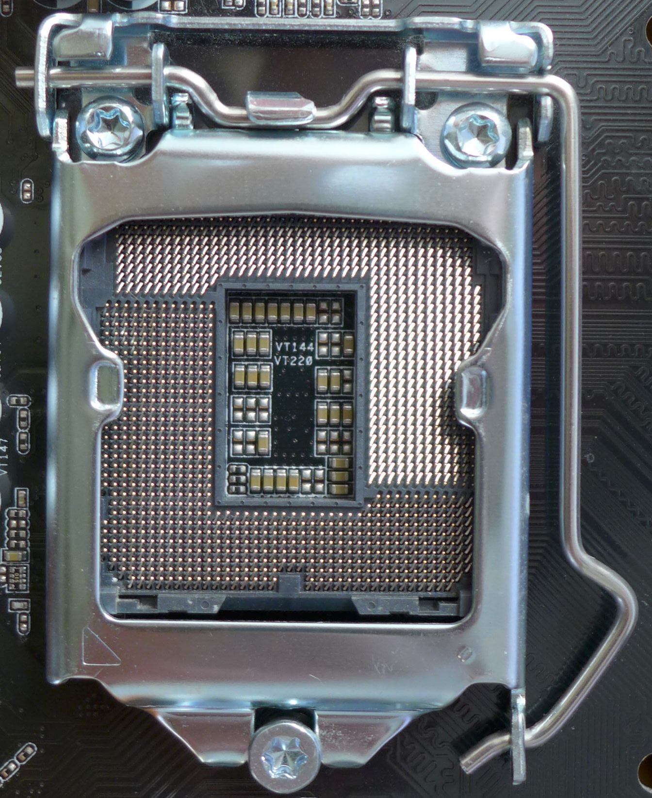
LGA 1151,[2] also known as Socket H4, is a type of zero insertion force flip-chip land grid array (LGA) socket for Intel desktop processors which comes in two distinct versions: the first revision which supports both Intel's Skylake[3] and Kaby Lake CPUs, and the second revision which supports Coffee Lake CPUs exclusively.
LGA 1151 is designed as a replacement for the LGA 1150 (known as Socket H3). LGA 1151 has 1151 protruding pins to make contact with the pads on the processor. The Fully Integrated Voltage Regulator, i.e. a voltage regulator which integrated on the CPU's die, introduced with Haswell and Broadwell, has again been moved to the motherboard.
Most motherboards for the first revision of the socket support solely DDR4 memory,[2] a lesser number support DDR3(L) memory,[4] and the least number have slots for both DDR4 or DDR3(L) but only one memory type can be installed.[5] Some have UniDIMM support, enabling either type of memory to be placed in the same DIMM, rather than having separate DDR3 and DDR4 DIMMs.[6] The second revision socket motherboards support only DDR4 memory.
Skylake, Kaby Lake, and Coffee Lake chipsets support VT-d, Intel Rapid Storage Technology, Intel Clear Video Technology, and Intel Wireless Display Technology (an appropriate CPU is required). Most motherboards with the LGA 1151 socket support varying video outputs (DVI, HDMI 1.4 or DisplayPort 1.2 – depending on the model). VGA output is optional since Intel dropped support for this video interface starting with Skylake.[7] HDMI 2.0 (4K@60 Hz) is only supported on motherboards equipped with Intel's Alpine Ridge Thunderbolt controller.[8]
Skylake, Kaby Lake, and Coffee Lake chipsets do not support the legacy conventional PCI interface; however, motherboard vendors may implement it using external chips.
Heatsink
[edit]The 4 holes for fastening the heatsink to the motherboard are placed in a square with a lateral length of 75 mm for Intel's sockets LGA 1156, LGA 1155, LGA 1150, LGA 1151 and LGA 1200. Cooling solutions should therefore be interchangeable.
LGA 1151 revision 1
[edit]DDR3 memory support
[edit]Intel officially states[9][10] that Skylake's and Kaby Lake's integrated memory controllers (IMC) support DDR3L memory modules only rated at 1.35 V and DDR4 at 1.2 V, which led to the speculation that higher voltages of DDR3 modules could damage or destroy the IMC and processor.[11] Meanwhile, ASRock, Gigabyte, and Asus guarantee that their Skylake and Kaby Lake DDR3 motherboards support DDR3 modules rated at 1.5 and 1.65V.[12][13][14]
Skylake chipsets (100 series and C230 series)
[edit]| H110 | B150 | Q150 | H170 | C236 | Q170 | Z170 | |||
|---|---|---|---|---|---|---|---|---|---|
| Overclocking | CPU (via BCLK[15] only;[16] might be disabled in new motherboards and BIOS releases[17]) + GPU + RAM (limited) | CPU (multiplier + BCLK[15]) + GPU + RAM | |||||||
| Kaby Lake CPUs support | Yes, after a BIOS update[18] | ||||||||
| Coffee Lake CPUs support | No | ||||||||
| Memory support | DDR4 (max. 32 GB total; 16 GB per slot) or | DDR4 (max. 64 GB total; 16 GB per slot) or | |||||||
| Maximum DIMM slots | 2 | 4 | |||||||
| Maximum USB ports | 2.0 | 6 | 4 | ||||||
| 3.0 | 4 | 6 | 8 | 10 | |||||
| Maximum SATA 3.0 ports | 4 | 6 | 8 | 6 | |||||
| Processor PCI Express v3.0 configuration | 1 ×16 | Either 1 ×16; 2 ×8; or 1 ×8 and 2 ×4 | |||||||
| PCH PCI Express configuration | 6 × 2.0 | 8 × 3.0 | 10 × 3.0 | 16 × 3.0 | 20 × 3.0 | ||||
| Independent Display Support (digital ports/pipes) |
3/2 | 3/3 | |||||||
| SATA RAID 0/1/5/10 support | No | Yes | Intel Rapid Storage Technology Enterprise | Yes | |||||
| Intel Active Management, Trusted Execution and vPro Technology | No | Yes | No | Yes | No | ||||
| Chipset TDP | 6 W | ||||||||
| Chipset lithography | 22 nm | ||||||||
| Release date | September 1, 2015[22][23] | Q3'15[24] | September 1, 2015[22][23] | Q4'15[25] | September 1, 2015[22][23] | August 5, 2015[26] | |||
Kaby Lake chipsets (200 series)
[edit]There is no equivalent Kaby Lake chipset analogous to the H110 chipset. Four additional PCH PCI-E lanes in Kaby Lake chipsets are reserved for implementing an M.2 slot to support Intel Optane Memory. Otherwise, corresponding Kaby Lake and Skylake chipsets are practically the same.[27]
Light blue indicates a difference between comparable Skylake and Kaby Lake chipsets.
| B250 | Q250 | H270 | Q270 | Z270 | ||
|---|---|---|---|---|---|---|
| Overclocking | No[28] | CPU (multiplier + BCLK[29]) + GPU + RAM | ||||
| Skylake CPUs support | Yes | |||||
| Coffee Lake CPUs support | No | |||||
| Memory support | DDR4 (max. 64 GB total; 16 GB per slot) or | |||||
| Maximum DIMM slots | 4 | |||||
| Maximum USB ports | 2.0 | 6 | 4 | |||
| 3.0 | 6 | 8 | 10 | |||
| Maximum SATA 3.0 ports | 6 | |||||
| Processor PCI Express v3.0 configuration | 1 ×16 | Either 1 ×16; 2 ×8; or 1 ×8 and 2 ×4 | ||||
| PCH PCI Express configuration | 12 × 3.0 | 14 × 3.0 | 20 × 3.0 | 24 × 3.0 | ||
| Independent Display Support (digital ports/pipes) |
3/3 | |||||
| SATA RAID 0/1/5/10 support | No | Yes | ||||
| Intel Active Management, Trusted Execution and vPro Technology | No | Yes | No | |||
| Intel Optane Memory Support | Yes, requires Core i3/i5/i7 CPU[31] | |||||
| Chipset TDP | 6 W[32] | |||||
| Chipset lithography | 22 nm[32] | |||||
| Release date | January 3, 2017[33] | |||||
LGA 1151 revision 2
[edit]The LGA 1151 socket was revised for the Coffee Lake generation CPUs and comes along with the Intel 300-series chipsets.[34] While physical dimensions remain unchanged, the updated socket reassigns some reserved pins, adding power and ground lines to support the requirements of 6-core and 8-core CPUs. The new socket also relocates the processor detection pin, breaking compatibility with earlier processors and motherboards. As a result, desktop Coffee Lake CPUs are officially not compatible with the 100 (original Skylake) and 200 (Kaby Lake) series chipsets.[35] Similarly, 300 series chipsets officially only support Coffee Lake and are not compatible with Skylake and Kaby Lake CPUs.
Socket 1151 rev 2 is sometimes also referred to as "1151-2".
Coffee Lake chipsets (300 series and C240 series)
[edit]Like with Kaby Lake chipsets, four additional PCH PCI-E lanes in Coffee Lake chipsets are reserved for implementing an M.2 slot to support Intel Optane Memory.
There's a 22 nm version of H310 chipset, H310C, which is sold only in China.[36] Motherboards based on this chipset support DDR3 memory as well.
| H310 | B365 | B360 | H370 | C246 | Q370 | Z370 | Z390 | ||
|---|---|---|---|---|---|---|---|---|---|
| Overclocking | No | CPU (multiplier + BCLK[37]) + GPU + RAM | |||||||
| Skylake/Kaby Lake CPUs support | No | ||||||||
| Coffee Lake (8th gen) CPUs support | Yes | ||||||||
| Coffee Lake Refresh (9th gen) CPUs support | Yes with BIOS update | Yes | Yes with BIOS update | Yes | |||||
| Memory [DDR4]
by Coffee Lake generation |
8th gen | Max. 32 GB total; 16 GB per slot | Max. 64 GB total; 16 GB per slot | ||||||
| 9th gen | Max. 64 GB total; 32 GB per slot | Max. 128 GB total; 32 GB per slot[38] | |||||||
| Maximum DIMM slots | 2 | 4 | |||||||
| Maximum USB 2.0 ports | 10 | 14 | 12 | 14 | |||||
| Maximum
USB 3.1 ports configuration |
Gen1 | 4 Ports | 8 Ports | 6 Ports | 8 Ports | 10 Ports | |||
| Gen2 | N/A | Up to 4 Ports | Up to 6 Ports | N/A | Up to 6 Ports | ||||
| Maximum SATA 3.0 ports | 4 | 6 | 8 | 6 | |||||
| Processor PCI Express v3.0 configuration | 1 ×16 | Either 1 ×16; 2 ×8; or 1 ×8 and 2 ×4 | |||||||
| PCH PCI Express configuration | 6 × 2.0 | 20 × 3.0 | 12 × 3.0 | 20 × 3.0 | 24 × 3.0 | ||||
| Independent Display Support (digital ports/pipes) | 3/2 | 3/3 | |||||||
| Integrated Wireless (802.11ac) | Yes** | No | Yes** | No | Yes** | ||||
| SATA RAID 0/1/5/10 support | No | Yes | No | Yes | Intel Rapid Storage Technology Enterprise | Yes | |||
| Intel Optane Memory Support | No | Yes, requires Core i3/i5/i7/i9 CPU | Yes, requires Core i3/i5/i7/i9 or Xeon E CPU | Yes, requires Core i3/i5/i7/i9 CPU | |||||
| Intel Smart Sound Technology | No | Yes | |||||||
| Chipset TDP | 6 W[39][40][41][42][43][44][45][46] | ||||||||
| Chipset lithography | 14 nm[39] | 22 nm[40] | 14 nm[41][42][43][44] | 22 nm[45] | 14 nm[46] | ||||
| Release date | April 2, 2018[47] | Q4'18 | April 2, 2018 | October 5, 2017[48] | October 8, 2018[49] | ||||
** depends on OEM's implementation
See also
[edit]References
[edit]- ^ "8th Generation Intel® Processor Family for S-Processor Platforms" (PDF).
- ^ a b Cutress, Ian (August 5, 2015). "Intel Skylake Z170 Motherboards: A Quick Look at 55+ New Products". AnandTech. Archived from the original on August 6, 2015. Retrieved August 5, 2015.
- ^ "MSI Z170A GAMING M7 (Intel LGA-1151) Review". TechpowerUp. August 5, 2015. Retrieved August 5, 2015.
- ^ "GIGABYTE - Motherboard - Socket 1151 - GA-Z170-HD3 DDR3 (rev. 1.0)". Gigabyte. Retrieved September 7, 2015.
- ^ "ASRock > B150M Combo-G". ASRock. Retrieved September 15, 2015.
- ^ Cutress, Ian (August 5, 2015). "The Intel 6th Gen Skylake Review: Core i7-6700K and i5-6600K Tested". AnandTech. Archived from the original on August 7, 2015. Retrieved August 5, 2015.
- ^ "Intel® Core™ i7-6700K Processor (8M Cache, up to 4.20 GHz)". intel. Retrieved August 6, 2015.
- ^ Cutress, Ian (August 5, 2015). "Intel Skylake Z170 Motherboards: A Quick Look at 55+ New Products". AnandTech. Archived from the original on August 6, 2015. Retrieved August 6, 2015.
- ^ "Intel® Core™ i7-6700K Processor (8M Cache, up to 4.20 GHz) Specifications". Intel. Retrieved February 6, 2016.
- ^ "Intel® Core™ i7-7700K Processor (8M Cache, up to 4.50 GHz) Product Specifications". Intel. Retrieved August 7, 2017.
- ^ Sexton, Michael Justin Allen (September 28, 2015). "Skylake's IMC Supports Only DDR3L". Tom's Hardware. Retrieved September 29, 2015.
- ^ "GIGABYTE - Motherboard - Socket 1151 - GA-Z170-HD3 DDR3 (rev. 1.0)". Gigabyte. Retrieved February 6, 2016.
- ^ "Fatal1ty Z170 Gaming K4/D3 Memory Support List". ASRock. Retrieved February 6, 2016.
- ^ Günsch, Michael (August 5, 2015). "Skylake-Mainboards: Asus präsentiert Z170-Platinen mit DDR3 bis 1,65 Volt". ComputerBase (in German). Retrieved February 6, 2016.
- ^ a b Cutress, Ian (August 5, 2015). "The Intel 6th Gen Skylake Review: Core i7-6700K and i5-6600K Tested". AnandTech. Archived from the original on August 5, 2015. Retrieved September 18, 2015.
- ^ "Asus H170-PLUS D3 Manual" (PDF). ASUS. Retrieved September 18, 2015.
- ^ Ung, Gordon (February 8, 2016). "It's official: Intel shuts down the cheap overclocking party by closing Skylake loophole". PCWorld. Retrieved February 9, 2016.
- ^ Wilson, Matthew (October 6, 2016). "MSI and Asus update motherboards with Kaby Lake support". KitGuru. Retrieved November 3, 2016.
- ^ a b Shilov, Anton (May 22, 2015). "Intel bids adieu to DDR3: Majority of 'Skylake-S' mainboards to use DDR4". KitGuru. Retrieved May 25, 2015.
- ^ "GIGABYTE - Motherboard - Socket 1151 - GA-Z170-HD3 DDR3 (rev. 1.0)". Gigabyte. Retrieved September 7, 2015.
- ^ "GIGABYTE - Motherboard - Socket 1151 - GA-Z170-HD3 DDR3 (rev. 1.0)". Gigabyte. Retrieved September 7, 2015.
- ^ a b c Sexton, Michael Justin Allen (September 2, 2015). "Asus Announces 10 New Motherboards Based On Latest 100-Series Intel Chipsets". Tom's Hardware. Retrieved October 3, 2015.
- ^ a b c "ASUS Announces H170, B150, H110 and Q170 Motherboard Series". ASUS. Retrieved October 3, 2015.
- ^ "Intel® Q150 Chipset (Intel® GL82Q150 PCH) Specifications". Intel. Retrieved December 26, 2015.
- ^ "Intel® C236 Chipset (Intel® GL82C236 PCH) Specifications". Intel. Retrieved December 26, 2015.
- ^ "Intel Unleashes Next-Gen Enthusiast Desktop PC Platform at Gamescom". Intel Newsroom. August 5, 2015. Retrieved August 5, 2015.
- ^ Shrout, Ryan (January 3, 2017). "The Intel Core i7-7700K Review - Kaby Lake and 14nm+ | Z270 Chipset and ASUS Maximus IX Code". PC Perspective. Archived from the original on February 6, 2019. Retrieved January 26, 2017.
- ^ Wallossek, Igor; Alcorn, Paul (January 3, 2017). "Intel Kaby Lake: Z270, Optane, Overclocking & HD Graphics 630". Tom's Hardware. Retrieved January 18, 2017.
- ^ Soderstrom, Thomas (November 29, 2016). "Overclocking Intel's Core i7-7700K: Kaby Lake Hits The Desktop!". Tom's Hardware. Retrieved January 18, 2017.
- ^ "B150M-C D3 | Motherboards". ASUS. Retrieved May 17, 2017.
- ^ "Intel® Optane™ Memory". Intel. Retrieved January 18, 2017.
- ^ a b "Intel® Z270 Chipset Specifications". Intel® ARK (Product Specs). Retrieved January 18, 2017.
- ^ Shenoy, Navin (January 3, 2017). "Get Ready for the Best New PCs for the New Year with New 7th Generation Intel Core Processors". Intel Newsroom. Retrieved January 18, 2017.
- ^ Cutress, Ian (October 5, 2017). "The AnandTech Coffee Lake Review: Initial Numbers on the Core i7-8700K and Core i5-8400". AnandTech. Archived from the original on October 5, 2017. Retrieved October 5, 2017.
- ^ Cutress, Ian (August 21, 2017). "Intel Launches 8th Generation Core CPUs, Starting with Kaby Lake Refresh for 15W Mobile". AnandTech. Archived from the original on August 21, 2017. Retrieved August 22, 2017.
- ^ Tyson, Mark (September 20, 2018). "Intel tech roll back: it is fabbing the new H310C chipset at 22nm". Hexus. Retrieved January 13, 2019.
- ^ Soderstrom, Thomas (November 5, 2017). "ASRock Z370 Taichi Benchmarks & Rating". Tom's Hardware. Retrieved April 3, 2018.
- ^ Cutress, Ian (October 15, 2018). "Intel to Support 128GB of DDR4 on Core 9th Gen Desktop Processors". AnandTech. Archived from the original on October 15, 2018. Retrieved October 23, 2018.
- ^ a b "Intel® H310 Chipset Product Specifications". Intel. Retrieved May 9, 2023.
- ^ a b "Intel® B365 Chipset Product Specifications". Intel. Retrieved May 9, 2023.
- ^ a b "Intel® B360 Chipset Product Specifications". Intel. Retrieved May 9, 2023.
- ^ a b "Intel® H370 Chipset Product Specifications". Intel. Retrieved May 9, 2023.
- ^ a b "Intel® C246 Chipset Product Specifications". Intel. Retrieved May 9, 2023.
- ^ a b "Intel® Q370 Chipset Product Specifications". Intel. Retrieved May 9, 2023.
- ^ a b "Intel® Z370 Chipset Product Specifications". Intel. Retrieved May 9, 2023.
- ^ a b "Intel® Z390 Chipset Product Specifications". Intel. Retrieved May 9, 2023.
- ^ Alcorn, Paul (April 3, 2018). "Intel Adds To Coffee Lake CPU Family, Outs New 300-Series Chipsets". Tom's Hardware. Retrieved April 3, 2018.
- ^ Cutress, Ian (October 5, 2017). "The AnandTech Coffee Lake Review: Initial Numbers on the Core i7-8700K and Core i5-8400". AnandTech. Archived from the original on October 5, 2017. Retrieved April 3, 2018.
- ^ Cutress, Ian (October 8, 2018). "Intel Announces 9th Gen Core CPUs: Core i9-9900K (8-Core), i7-9700K, & i5-9600K". AnandTech. Archived from the original on October 8, 2018. Retrieved October 8, 2018.
Grokipedia
LGA 1151
View on GrokipediaIntroduction
Background and Development
LGA 1151 was introduced by Intel in August 2015 as the successor to the LGA 1150 socket, debuting alongside the sixth-generation Core processors based on the Skylake microarchitecture.[5] This new socket design facilitated the transition from the previous generation's architecture, enabling support for DDR4 memory while maintaining compatibility with low-voltage DDR3L in early implementations.[6] The development of LGA 1151 aligned with Intel's Tick-Tock model, where Skylake represented the "Tock" phase—a major architectural redesign on the established 14 nm process node—following the "Tick" of Broadwell, which had introduced a die shrink but faced production delays.[7] The socket's primary purposes included enhancing power efficiency through refined microarchitectural improvements and preparing the platform for future scalability in core counts, addressing the limitations of prior sockets that capped mainstream desktop processors at four cores. Revision 1 of LGA 1151, launched in 2015, supported Skylake and subsequent Kaby Lake processors, focusing on balanced performance for consumer and business applications.[2] In 2017, Intel released Revision 2 of the LGA 1151 socket to accommodate the Coffee Lake microarchitecture, which increased core counts to six in mainstream models and required updated 300-series chipsets for compatibility.[8] This revision extended the socket's lifecycle while resolving earlier constraints on multi-core performance.[9] Support for LGA 1151 began to phase out following the release of the ninth-generation Coffee Lake Refresh processors in 2018, marking the final major update, culminating in its full replacement by the LGA 1200 socket in 2020 alongside the tenth-generation Comet Lake processors.[2][10]General Characteristics
The LGA 1151, also known as Socket H4 or FCLGA1151, is a land grid array (LGA) CPU socket featuring 1151 pins arranged in a 40×40 grid configuration, with certain positions reserved or depopulated to accommodate electrical and mechanical requirements.[3] This design facilitates direct electrical contact between the processor package and the motherboard, enabling efficient signal transmission for high-performance computing tasks. The socket employs a zero insertion force (ZIF) lever mechanism, which allows processors to be installed and removed without applying pressure to the pins, thereby minimizing the risk of damage during handling.[11] The contact area of the LGA 1151 measures 37.5 mm × 37.5 mm, providing a compact footprint suitable for standard ATX and micro-ATX motherboard layouts.[12] Electrically, it supports a core voltage (VCC) range of 0.55 V to 1.52 V, allowing for dynamic voltage scaling to balance performance and power efficiency across varying workloads. Power delivery is rated for thermal design power (TDP) up to 95 W for standard processors, with unlocked variants capable of reaching 125 W under overclocked conditions, necessitating appropriate cooling solutions to maintain thermal limits.[13] In terms of signaling interfaces, the LGA 1151 supports a dual-channel DDR4 memory interface, enabling data rates starting at 2133 MT/s and scalable to higher speeds depending on the processor generation.[14] It also provides up to 16 lanes of PCIe 3.0 directly from the CPU, supporting configurations such as x16 for graphics cards or bifurcated x8/x8 setups for multi-GPU or storage applications.[14] The socket is designed primarily for desktop Intel Core, Pentium, Celeron, and Xeon E3 v5/v6 and E-2100 series processors, ensuring compatibility with mainstream computing platforms.[1] While the two revisions of the LGA 1151 share these core traits, they differ in specific pin assignments to support evolving processor architectures.Physical Specifications
Socket Design
The LGA 1151 socket employs a land grid array (LGA) configuration with 1,151 surface-mount pins that interface with the matching land pads on the FCLGA1151 processor package, enabling a zero-insertion-force connection for reliable electrical and mechanical coupling. The socket is implemented using ball grid array (BGA) packaging on the motherboard, allowing for direct soldering and high-density integration without through-hole mounting. This design facilitates efficient heat dissipation and compact board layouts by distributing the pins across the socket base.[15] The pin layout features a central 37.5 × 37.5 mm active area housing the primary signal pins for data transfer, address lines, and control signals, while power (Vcc) and ground (Vss) pins are strategically distributed in outer planes to minimize inductance and ensure stable voltage delivery under load. With a uniform pin pitch of 0.914 mm, the arrangement supports high-speed signaling while adhering to manufacturing tolerances for precise alignment. The overall processor contact area measures 37.5 mm × 37.5 mm, optimizing compatibility with standard desktop motherboards.[13] Installation involves aligning the processor using its corner notches and the gold triangle indicator (marking pin 1 location) with corresponding guides on the socket to prevent misalignment or damage. The CPU is then lowered onto the pins, and the integrated load mechanism—a lever-based retention arm—is engaged to apply uniform downward pressure, securing the package without requiring manual force on the contacts. This process ensures intimate pin-to-land contact for optimal performance. The socket is rated for at least 20 insertion and removal cycles, providing durability for typical upgrade scenarios.[16][17] Compared to its predecessor, the LGA 1150 socket, the LGA 1151 maintains the same 0.914 mm pin pitch but refines the mechanical keying and contact distribution for enhanced signal integrity in higher-frequency operations. The socket includes four peripheral mounting holes compatible with standard heatsink retention brackets for secure thermal solution attachment.[16]Heatsink Interface
The heatsink interface for the LGA 1151 socket employs a standard mounting mechanism featuring four threaded standoffs arranged in a square pattern with 75 mm × 75 mm hole spacing, allowing secure attachment to the motherboard.[18] This design facilitates even distribution of force across the socket area during installation.[19] To achieve optimal thermal contact, the interface requires applying 30–50 lbf (pounds force) of mounting force through a backplate and retention bracket, ensuring the heatsink base presses uniformly against the CPU without exceeding structural limits.[20] The thermal interface itself relies on direct contact between the heatsink base and the processor's integrated heat spreader (IHS), typically facilitated by a thin layer of thermal compound to minimize air gaps and enhance heat transfer efficiency.[11] This setup maintains compatibility with Intel's reference coolers, such as the Laminar RM1 series, as well as a wide array of third-party air and liquid cooling solutions designed for LGA 115x sockets, provided they adhere to the mounting dimensions and pressure guidelines.[21] The Independent Loading Mechanism (ILM) mirrors that of the preceding LGA 1150 socket, promoting straightforward upgrades while being refined to handle elevated thermal design power (TDP) demands of supported processors.[22] A noted challenge in implementation is the risk of CPU IHS warping or socket pin damage from uneven or excessive mounting pressure, particularly during overtightening; aftermarket coolers often incorporate reinforced backplates to mitigate this by promoting balanced load distribution and preventing motherboard flex.[20]Revision 1
Supported Processors
The LGA 1151 Revision 1 socket supports Intel's 6th and 7th generation Core desktop processors, codenamed Skylake and Kaby Lake, respectively. These processors are fabricated on Intel's 14 nm process and integrate Intel HD Graphics 530 (Skylake) or 630 (Kaby Lake) in non-F variants, with "K" models featuring unlocked multipliers for overclocking. Intel released numerous desktop SKUs across both generations, spanning Core i3, i5, i7 families, as well as Pentium and Celeron options.[23][24] The 6th generation Skylake processors launched on August 5, 2015, introducing DDR4 memory support to mainstream desktops. They feature up to 4 cores and 8 threads, with thermal design powers (TDP) of 35 W to 91 W. Key features include support for DDR4-2133 memory and up to 16 PCIe 3.0 lanes from the CPU. Representative desktop models are summarized below:| Model | Cores/Threads | Base/Turbo Frequency | TDP | Integrated Graphics | Launch Date |
|---|---|---|---|---|---|
| Core i7-6700K | 4/8 | 4.0 GHz / 4.2 GHz | 91 W | HD 530 | Q3'15 |
| Core i5-6600K | 4/4 | 3.5 GHz / 3.9 GHz | 91 W | HD 530 | Q3'15 |
| Core i5-6500 | 4/4 | 3.2 GHz / 3.6 GHz | 65 W | HD 530 | Q3'15 |
| Core i3-6100 | 2/4 | 3.7 GHz / 3.7 GHz | 51 W | HD 530 | Q3'15 |
| Model | Cores/Threads | Base/Turbo Frequency | TDP | Integrated Graphics | Launch Date |
|---|---|---|---|---|---|
| Core i7-7700K | 4/8 | 4.2 GHz / 4.5 GHz | 91 W | HD 630 | Q1'17 |
| Core i5-7600K | 4/4 | 3.8 GHz / 4.2 GHz | 91 W | HD 630 | Q1'17 |
| Core i5-7500 | 4/4 | 3.4 GHz / 3.8 GHz | 65 W | HD 630 | Q1'17 |
| Core i3-7100 | 2/4 | 3.9 GHz / 3.9 GHz | 51 W | HD 630 | Q1'17 |
Chipset Support
The Intel 100 Series chipsets were designed for the first revision of the LGA 1151 socket, supporting Skylake processors, while the 200 Series chipsets, launched in 2017, added support for Kaby Lake on updated BIOS. These include enthusiast Z170/Z270, mid-range H170/H270, value B150/B250, entry-level H110, business Q170/Q270, and others like Q150. They provide connectivity via the DMI 3.0 x4 interface (8 GT/s).[25][26]| Chipset | Target Market | Key Differentiators |
|---|---|---|
| Z170/Z270 | Enthusiast | CPU overclocking support; up to 10 USB 3.0 ports; 20 PCIe 2.0 lanes from chipset; memory OC up to DDR4-2133/2400.[25] |
| H170/H270 | Mid-range | No CPU overclocking; up to 8 USB 3.0 ports; 16 PCIe 2.0 lanes; vPro on select models. |
| B150/B250 | Value | No overclocking; up to 6 USB 3.0 ports; 12 PCIe 2.0 lanes; basic expansion.[27] |
| H110 | Basic | Entry-level, no overclocking; 4 USB 3.0 ports; 6 PCIe 2.0 lanes; minimal features. |
| Q170/Q270 | Business | vPro and stability; up to 8 USB 3.0 ports; 16 PCIe 2.0 lanes; no overclocking. |
Memory and I/O Features
The Revision 1 of the LGA 1151 socket, supporting 6th and 7th generation Intel Core processors, features a dual-channel integrated memory controller handling DDR4 at up to 2133 MHz (Skylake) or 2400 MHz (Kaby Lake), with a maximum capacity of 64 GB. Early boards supported DDR3L-1600, but DDR4 is standard; ECC is available on Xeon E3 v5/v6 models.[23] I/O is managed by 100/200-series chipsets via DMI 3.0 x4 at 8 GT/s. USB support reaches up to 10 ports (USB 3.0 Gen1 at 5 Gbps), plus 14 USB 2.0. Storage includes 6 SATA III ports with RAID options via Intel RST. Integrated graphics (HD 530/630) support up to 3 displays and Quick Sync Video for media acceleration. PCIe provides 16 lanes (3.0) from CPU for GPUs/SSD, plus 6-20 lanes (2.0) from chipset. Premium boards may add USB 3.1 or 10 GbE via controllers. These features suit efficient multitasking but offer less bandwidth than Revision 2 for higher-core workloads.[25]Revision 2
Supported Processors
The LGA 1151 Revision 2 socket supports Intel's 8th and 9th generation Core desktop processors, codenamed Coffee Lake and Coffee Lake Refresh, respectively, which introduced higher core counts compared to prior generations while maintaining compatibility with 300-series chipsets. These processors are fabricated on Intel's 14 nm process and integrate Intel UHD Graphics 630 in non-F variants, with "K" and "KF" models featuring unlocked multipliers for overclocking. Across both generations, Intel released over 60 desktop SKUs, spanning Core i3, i5, i7, and i9 families, as well as Pentium Gold and Celeron options.[31] The 8th generation Coffee Lake processors launched on October 5, 2017, marking the first mainstream desktop Intel CPUs with 6 cores in i5 and i7 models. They support up to 6 cores and 12 threads, with thermal design powers (TDP) of 65 W for standard models and 95 W for unlocked variants. Key features include support for DDR4-2666 memory and up to 16 PCIe 3.0 lanes from the CPU. Representative desktop models are summarized below:| Model | Cores/Threads | Base/Turbo Frequency | TDP | Integrated Graphics | Launch Date |
|---|---|---|---|---|---|
| Core i3-8350K | 4/4 | 4.0 GHz / 4.0 GHz | 91 W | UHD 630 | Q4'17 |
| Core i5-8400 | 6/6 | 2.8 GHz / 4.0 GHz | 65 W | UHD 630 | Q4'17 |
| Core i5-8600K | 6/6 | 3.6 GHz / 4.3 GHz | 95 W | UHD 630 | Q4'17 |
| Core i7-8700 | 6/12 | 3.2 GHz / 4.6 GHz | 65 W | UHD 630 | Q4'17 |
| Core i7-8700K | 6/12 | 3.7 GHz / 4.7 GHz | 95 W | UHD 630 | Q4'17 |
| Model | Cores/Threads | Base/Turbo Frequency | TDP | Integrated Graphics | Launch Date |
|---|---|---|---|---|---|
| Core i3-9100 | 4/4 | 3.6 GHz / 4.2 GHz | 65 W | UHD 630 | Q4'18 |
| Core i5-9600K | 6/6 | 3.7 GHz / 4.6 GHz | 95 W | UHD 630 | Q4'18 |
| Core i7-9700K | 8/8 | 3.6 GHz / 4.9 GHz | 95 W | UHD 630 | Q4'18 |
| Core i9-9900K | 8/16 | 3.6 GHz / 5.0 GHz | 95 W | UHD 630 | Q4'18 |
| Core i9-9900KF | 8/16 | 3.6 GHz / 5.0 GHz | 95 W | None | Q4'18 |
Chipset Support
The Intel 300 Series chipsets were designed specifically for the second revision of the LGA 1151 socket, supporting Coffee Lake and later processors. These chipsets include the enthusiast-oriented Z370 and its refresh Z390, mid-range H370, value B360, entry-level H310, business-focused Q370, and workstation C242. Launched between late 2017 and early 2018, they introduced enhanced connectivity over prior generations while maintaining the LGA 1151 form factor.[30][33]| Chipset | Target Market | Key Differentiators |
|---|---|---|
| Z370 | Enthusiast | Supports CPU overclocking; up to 14 USB 3.1 ports; full 24 PCIe 3.0 lanes from chipset.[30] |
| Z390 | Enthusiast (Refresh) | Enhanced overclocking with native USB 3.1 Gen 2 support; compatible with 9th-gen processors; 24 PCIe 3.0 lanes. |
| H370 | Mid-range | No CPU overclocking; up to 14 USB 3.1 ports; 24 PCIe 3.0 lanes; vPro support for business features. |
| B360 | Value | No overclocking; up to 12 USB 3.1 ports; 12 PCIe 3.0 lanes; balanced for mainstream builds.[34] |
| H310 | Basic | Entry-level with no overclocking; up to 10 USB 3.1 ports; 6 PCIe 3.0 lanes; minimal expansion. |
| Q370 | Business | vPro and stability features; up to 14 USB 3.1 ports; 24 PCIe 3.0 lanes; no overclocking. |
| C242 | Workstation | ECC memory support; up to 14 USB 3.1 ports; 24 PCIe 3.0 lanes; optimized for professional workloads. |