Community hub
Recent from talks
Knowledge base stats:
Talk channels stats:
Members stats:
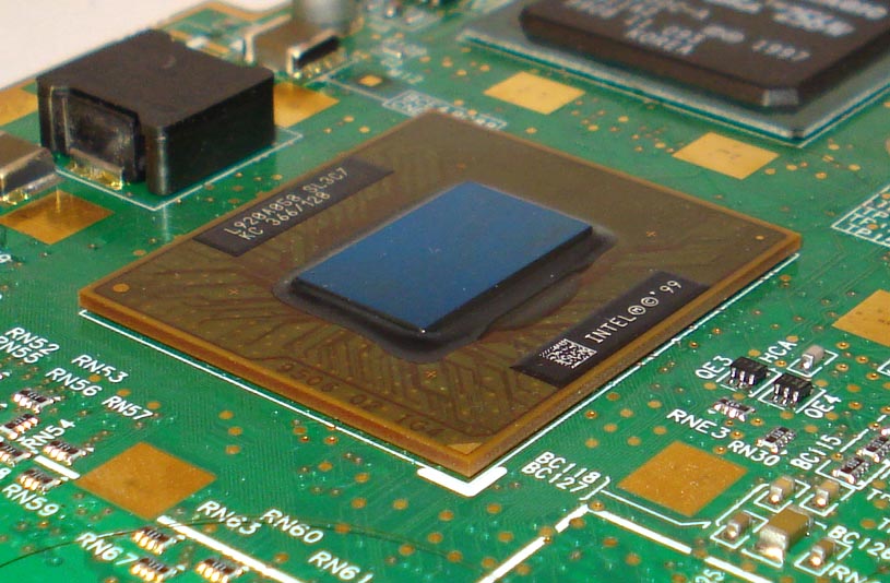
Flip chip
Flip chip, also known as controlled collapse chip connection or its abbreviation, C4, is a method for interconnecting dies such as semiconductor devices, IC chips, integrated passive devices and microelectromechanical systems (MEMS), to external circuitry with solder bumps that have been deposited onto the chip pads. The technique was developed by General Electric's Light Military Electronics Department, Utica, New York. The solder bumps are deposited on the chip pads on the top side of the wafer during the final wafer processing step. In order to mount the chip to external circuitry (e.g., a circuit board or another chip or wafer), it is flipped over so that its top side faces down, and aligned so that its pads align with matching pads on the external circuit, and then the solder is reflowed to complete the interconnect. This is in contrast to wire bonding, in which the chip is mounted upright and fine wires are welded onto the chip pads and lead frame contacts to interconnect the chip pads to external circuitry.
In typical semiconductor fabrication systems, chips are built up in large numbers on a single large wafer of semiconductor material, typically silicon. The individual chips are patterned with small pads of metal near their edges that serve as the connections to an eventual mechanical carrier. The chips are then cut out of the wafer and attached to their carriers, typically via wire bonding such as thermosonic bonding. These wires eventually lead to pins on the outside of the carriers, which are attached to the rest of the circuitry making up the electronic system.
Processing a flip chip is similar to conventional IC fabrication, with a few additional steps. Near the end of the manufacturing process, the attachment pads are metalized to make them more receptive to solder. This typically consists of several treatments. A small dot of solder is then deposited on each metalized pad. The chips are then cut out of the wafer as normal.
To attach the flip chip into a circuit, the chip is inverted to bring the solder dots down onto connectors or pads on the underlying electronics or circuit board or substrate. The solder is then re-melted to produce an electrical connection, typically using a thermosonic bonding or alternatively reflow solder process.
This also leaves a small space between the chip's circuitry and the underlying mounting. In many cases an electrically-insulating adhesive is then "underfilled" to provide a stronger mechanical connection, provide a heat bridge, and to ensure the solder joints are not stressed due to differential heating of the chip and the rest of the system. The underfill distributes the thermal expansion mismatch between the chip and the board, preventing stress concentration in the solder joints which would lead to premature failure.
Solder balls can be mounted on the chips by separately making the balls and then attaching them to the chips by using a vacuum pick up device to pick up the balls and then placing them into a chip with flux applied on contact pads for the balls, or by wafer bumping which consists of electroplating in which seed metals are first deposited onto a wafer with the chips to be bumped. This allows the solder to adhere to the contact pads of the chips during the electroplating process. The seed metals are alloys and are deposited by sputtering onto the wafer with the chips to be bumped. A photoresist mask is used to only deposit the seed metal on top of the contact pads of the chips. The wafer then undergoes electroplating, and the photoresist layer is removed or stripped. Then the solder on the chips undergoes solder reflow to form the bumps into their final shape. Solder balls are often 75 to 500 microns in diameter.
In 2008, High-speed mounting methods evolved through a cooperation between Reel Service Ltd. and Siemens AG in the development of a high speed mounting tape known as 'MicroTape'[1]. By adding a tape-and-reel process into the assembly methodology, placement at high speed is possible, achieving a 99.90% pick rate and a placement rate of 21,000 cph (components per hour), using standard PCB assembly equipment.
Flip-chip packages often consist of a silicon die sitting on top of a "substrate" which then sits on top of a traditional PCB. The substrate can have a Ball Grid Array (BGA) on its underside. The substrate makes the connections to the die available for use by the PCB. Substates made with build up film such as Ajinomoto Build up Film (ABF), are manufactured around a core, and the film is stacked on the core in layers by vacuum lamination at high temperatures. After each layer is applied, the film is cured, and laser vias are made with CO2 or UV lasers, then the blind vias in the substrate are cleaned and the build up film is roughened chemically with a permanganate, and then copper is deposited using electroless copper plating, followed by creating a pattern on the copper using photolithography and etching, and then this process is repeated for every layer of the substrate.
Hub AI
Flip chip AI simulator
(@Flip chip_simulator)
Flip chip
Flip chip, also known as controlled collapse chip connection or its abbreviation, C4, is a method for interconnecting dies such as semiconductor devices, IC chips, integrated passive devices and microelectromechanical systems (MEMS), to external circuitry with solder bumps that have been deposited onto the chip pads. The technique was developed by General Electric's Light Military Electronics Department, Utica, New York. The solder bumps are deposited on the chip pads on the top side of the wafer during the final wafer processing step. In order to mount the chip to external circuitry (e.g., a circuit board or another chip or wafer), it is flipped over so that its top side faces down, and aligned so that its pads align with matching pads on the external circuit, and then the solder is reflowed to complete the interconnect. This is in contrast to wire bonding, in which the chip is mounted upright and fine wires are welded onto the chip pads and lead frame contacts to interconnect the chip pads to external circuitry.
In typical semiconductor fabrication systems, chips are built up in large numbers on a single large wafer of semiconductor material, typically silicon. The individual chips are patterned with small pads of metal near their edges that serve as the connections to an eventual mechanical carrier. The chips are then cut out of the wafer and attached to their carriers, typically via wire bonding such as thermosonic bonding. These wires eventually lead to pins on the outside of the carriers, which are attached to the rest of the circuitry making up the electronic system.
Processing a flip chip is similar to conventional IC fabrication, with a few additional steps. Near the end of the manufacturing process, the attachment pads are metalized to make them more receptive to solder. This typically consists of several treatments. A small dot of solder is then deposited on each metalized pad. The chips are then cut out of the wafer as normal.
To attach the flip chip into a circuit, the chip is inverted to bring the solder dots down onto connectors or pads on the underlying electronics or circuit board or substrate. The solder is then re-melted to produce an electrical connection, typically using a thermosonic bonding or alternatively reflow solder process.
This also leaves a small space between the chip's circuitry and the underlying mounting. In many cases an electrically-insulating adhesive is then "underfilled" to provide a stronger mechanical connection, provide a heat bridge, and to ensure the solder joints are not stressed due to differential heating of the chip and the rest of the system. The underfill distributes the thermal expansion mismatch between the chip and the board, preventing stress concentration in the solder joints which would lead to premature failure.
Solder balls can be mounted on the chips by separately making the balls and then attaching them to the chips by using a vacuum pick up device to pick up the balls and then placing them into a chip with flux applied on contact pads for the balls, or by wafer bumping which consists of electroplating in which seed metals are first deposited onto a wafer with the chips to be bumped. This allows the solder to adhere to the contact pads of the chips during the electroplating process. The seed metals are alloys and are deposited by sputtering onto the wafer with the chips to be bumped. A photoresist mask is used to only deposit the seed metal on top of the contact pads of the chips. The wafer then undergoes electroplating, and the photoresist layer is removed or stripped. Then the solder on the chips undergoes solder reflow to form the bumps into their final shape. Solder balls are often 75 to 500 microns in diameter.
In 2008, High-speed mounting methods evolved through a cooperation between Reel Service Ltd. and Siemens AG in the development of a high speed mounting tape known as 'MicroTape'[1]. By adding a tape-and-reel process into the assembly methodology, placement at high speed is possible, achieving a 99.90% pick rate and a placement rate of 21,000 cph (components per hour), using standard PCB assembly equipment.
Flip-chip packages often consist of a silicon die sitting on top of a "substrate" which then sits on top of a traditional PCB. The substrate can have a Ball Grid Array (BGA) on its underside. The substrate makes the connections to the die available for use by the PCB. Substates made with build up film such as Ajinomoto Build up Film (ABF), are manufactured around a core, and the film is stacked on the core in layers by vacuum lamination at high temperatures. After each layer is applied, the film is cured, and laser vias are made with CO2 or UV lasers, then the blind vias in the substrate are cleaned and the build up film is roughened chemically with a permanganate, and then copper is deposited using electroless copper plating, followed by creating a pattern on the copper using photolithography and etching, and then this process is repeated for every layer of the substrate.