Reflection high-energy electron diffraction
Main page

Reflection high-energy electron diffraction

logo
Community Hub0 subscribers
Read side by side
from Wikipedia

Reflection high-energy electron diffraction (RHEED) is a technique used to characterize the surface of crystalline materials. RHEED systems gather information only from the surface layer of the sample, which distinguishes RHEED from other materials characterization methods that also rely on diffraction of high-energy electrons. Transmission electron microscopy, another common electron diffraction method samples mainly the bulk of the sample due to the geometry of the system, although in special cases it can provide surface information. Low-energy electron diffraction (LEED) is also surface sensitive, but LEED achieves surface sensitivity through the use of low energy electrons.

Introduction

[edit]

A RHEED system requires an electron source (gun), photoluminescent detector screen and a sample with a clean surface, although modern RHEED systems have additional parts to optimize the technique.[1][2] The electron gun generates a beam of electrons which strike the sample at a very small angle relative to the sample surface. Incident electrons diffract from atoms at the surface of the sample, and a small fraction of the diffracted electrons interfere constructively at specific angles and form regular patterns on the detector. The electrons interfere according to the position of atoms on the sample surface, so the diffraction pattern at the detector is a function of the sample surface. Figure 1 shows the most basic setup of a RHEED system.

Figure 1. Systematic setup of the electron gun, sample and detector/CCD components of a RHEED system. Electrons follow the path indicated by the arrow and approach the sample at angle θ. The sample surface diffracts electrons, and some of these diffracted electrons reach the detector and form the RHEED pattern. The reflected (specular) beam follows the path from the sample to the detector.

Surface diffraction

[edit]

In the RHEED setup, only atoms at the sample surface contribute to the RHEED pattern.[3] The glancing angle of incident electrons allows them to escape the bulk of the sample and to reach the detector. Atoms at the sample surface diffract (scatter) the incident electrons due to the wavelike properties of electrons.

The diffracted electrons interfere constructively at specific angles according to the crystal structure and spacing of the atoms at the sample surface and the wavelength of the incident electrons. Some of the electron waves created by constructive interference collide with the detector, creating specific diffraction patterns according to the surface features of the sample. Users characterize the crystallography of the sample surface through analysis of the diffraction patterns. Figure 2 shows a RHEED pattern. Video 1 depicts a metrology instrument recording the RHEED intensity oscillations and deposition rate for process control and analysis.

Figure 2. A RHEED pattern obtained from electron diffraction from a clean TiO2 (110) surface. The bright spots indicate where many electrons reach the detector. The lines that can be observed are Kikuchi Lines.


Two types of diffraction contribute to RHEED patterns. Some incident electrons undergo a single, elastic scattering event at the crystal surface, a process termed kinematic scattering.[1] Dynamic scattering occurs when electrons undergo multiple diffraction events in the crystal and lose some of their energy due to interactions with the sample.[1] Users extract non-qualitative data from the kinematically diffracted electrons. These electrons account for the high intensity spots or rings common to RHEED patterns. RHEED users also analyze dynamically scattered electrons with complex techniques and models to gather quantitative information from RHEED patterns.[3]

Kinematic scattering analysis

[edit]

RHEED users construct Ewald's spheres to find the crystallographic properties of the sample surface. Ewald's spheres show the allowed diffraction conditions for kinematically scattered electrons in a given RHEED setup. The diffraction pattern at the screen relates to the Ewald's sphere geometry, so RHEED users can directly calculate the reciprocal lattice of the sample with a RHEED pattern, the energy of the incident electrons and the distance from the detector to the sample. The user must relate the geometry and spacing of the spots of a perfect pattern to the Ewald's sphere in order to determine the reciprocal lattice of the sample surface.

The Ewald's sphere analysis is similar to that for bulk crystals, however the reciprocal lattice for the sample differs from that for a 3D material due to the surface sensitivity of the RHEED process. The reciprocal lattices of bulk crystals consist of a set of points in 3D space. However, only the first few layers of the material contribute to the diffraction in RHEED, so there are no diffraction conditions in the dimension perpendicular to the sample surface. Due to the lack of a third diffracting condition, the reciprocal lattice of a crystal surface is a series of infinite rods extending perpendicular to the sample's surface.[4] These rods originate at the conventional 2D reciprocal lattice points of the sample's surface.

The Ewald's sphere is centered on the sample surface with a radius equal to the magnitude of the wavevector of the incident electrons,

,

where λ is the electrons' de Broglie wavelength.

Figure 3. The construction of the Ewald's sphere for elastic diffraction in RHEED. The radius of the Ewald's sphere is equal to the magnitude of the incoming electron's wave vector ki, which ends at the origin of the two-dimensional reciprocal lattice. The wave vector of the outgoing electron khl corresponds to an allowed diffraction condition, and the difference between the components parallel to the surface of the two wave vectors is the reciprocal lattice vector Ghl.

Diffraction conditions are satisfied where the rods of reciprocal lattice intersect the Ewald's sphere. Therefore, the magnitude of a vector from the origin of the Ewald's sphere to the intersection of any reciprocal lattice rods is equal in magnitude to that of the incident beam. This is expressed as

(2)

Here, khl is the wave vector of the elastically diffracted electrons of the order (hl) at any intersection of reciprocal lattice rods with Ewald's sphere

The projections of the two vectors onto the plane of the sample's surface differ by a reciprocal lattice vector Ghl,

(3)
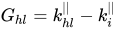
Figure 3 shows the construction of the Ewald's sphere and provides examples of the G, khl and ki vectors.

Many of the reciprocal lattice rods meet the diffraction condition, however the RHEED system is designed such that only the low orders of diffraction are incident on the detector. The RHEED pattern at the detector is a projection only of the k vectors that are within the angular range that contains the detector. The size and position of the detector determine which of the diffracted electrons are within the angular range that reaches the detector, so the geometry of the RHEED pattern can be related back to the geometry of the reciprocal lattice of the sample surface through use of trigonometric relations and the distance from the sample to detector.

The k vectors are labeled such that the vector k00 that forms the smallest angle with the sample surface is called the 0th order beam.[3] The 0th order beam is also known as the specular beam. Each successive intersection of a rod and the sphere further from the sample surface is labeled as a higher order reflection. Because of the way the center of the Ewald's sphere is positioned, the specular beam forms the same angle with the substrate as the incident electron beam. The specular point has the greatest intensity on a RHEED pattern and is labeled as the (00) point by convention.[3] The other points on the RHEED pattern are indexed according to the reflection order they project.

The radius of the Ewald's sphere is much larger than the spacing between reciprocal lattice rods because the incident beam has a very short wavelength due to its high-energy electrons. Rows of reciprocal lattice rods actually intersect the Ewald's sphere as an approximate plane because identical rows of parallel reciprocal lattice rods sit directly in front and behind the single row shown.[1] Figure 3 shows a cross sectional view of a single row of reciprocal lattice rods filling of the diffraction conditions. The reciprocal lattice rods in Figure 3 show the end on view of these planes, which are perpendicular to the computer screen in the figure.

The intersections of these effective planes with the Ewald's sphere forms circles, called Laue circles. The RHEED pattern is a collection of points on the perimeters of concentric Laue circles around the center point. However, interference effects between the diffracted electrons still yield strong intensities at single points on each Laue circle. Figure 4 shows the intersection of one of these planes with the Ewald's Sphere.

Figure 4. Diffraction from a row of atoms a Laue circle on the surface of the Ewald's sphere. The reciprocal lattice rods are so closely space, that they comprise the plane cutting the sphere. Diffraction conditions are fulfilled on the perimeter of the Laue circle. The vectors are all equal to the reciprocal of the incident vector, k.

The azimuthal angle affects the geometry and intensity of RHEED patterns.[4] The azimuthal angle is the angle at which the incident electrons intersect the ordered crystal lattice on the surface of the sample. Most RHEED systems are equipped with a sample holder that can rotate the crystal around an axis perpendicular to the sample surface. RHEED users rotate the sample to optimize the intensity profiles of patterns. Users generally index at least 2 RHEED scans at different azimuth angles for reliable characterization of the crystal's surface structure.[4] Figure 5 shows a schematic diagram of an electron beam incident on the sample at different azimuth angles.

Figure 5. The incident electron beam is incident on an identical surface structure at a different azimuth angles in a) and b). The sample is viewed from the top in the figure, and the points correspond to the reciprocal lattice rods, which extend out of the screen. The RHEED pattern would be different for each azimuth angle.

Users sometimes rotate the sample around an axis perpendicular to the sampling surface during RHEED experiments to create a RHEED pattern called the azimuthal plot.[4] Rotating the sample changes the intensity of the diffracted beams due to their dependence on the azimuth angle.[5] RHEED specialists characterize film morphologies by measuring the changes in beam intensity and comparing these changes to theoretical calculations, which can effectively model the dependence of the intensity of diffracted beams on the azimuth angle.[5]

Dynamic scattering analysis

[edit]

The dynamically, or inelastically, scattered electrons provide several types of information about the sample as well. The brightness or intensity at a point on the detector depends on dynamic scattering, so all analysis involving the intensity must account for dynamic scattering.[1][3] Some inelastically scattered electrons penetrate the bulk crystal and fulfill Bragg diffraction conditions. These inelastically scattered electrons can reach the detector to yield Kikuchi diffraction patterns, which are useful for calculating diffraction conditions.[3] Kikuchi patterns are characterized by lines connecting the intense diffraction points on a RHEED pattern. Figure 6 shows a RHEED pattern with visible Kikuchi lines.

Figure 6. A RHEED pattern from a TiO2 (110) surface with visible Kikuchi lines. The Kikuchi lines pass through the Laue circles and appear to radiate from the center of the pattern.

RHEED system requirements

[edit]

Electron gun

[edit]

The electron gun is one of the most important piece of equipment in a RHEED system.[1] The gun limits the resolution and testing limits of the system. Tungsten filaments are the primary electron source for the electron gun of most RHEED systems due to the low work function of tungsten. In the typical setup, the tungsten filament is the cathode and a positively biased anode draws electrons from the tip of the tungsten filament.[1]

The magnitude of the anode bias determines the energy of the incident electrons. The optimal anode bias is dependent upon the type of information desired. At large incident angles, electrons with high energy can penetrate the surface of the sample and degrade the surface sensitivity of the instrument.[1] However, the dimensions of the Laue zones are proportional to the inverse square of the electron energy meaning that more information is recorded at the detector at higher incident electron energies.[1] For general surface characterization, the electron gun is operated the range of 10-30 keV.[3]

In a typical RHEED setup, one magnetic and one electric field focus the incident beam of electrons.[1] A negatively biased Wehnelt electrode positioned between the cathode filament and anode applies a small electric field, which focuses the electrons as they pass through the anode. An adjustable magnetic lens focuses the electrons onto the sample surface after they pass through the anode. A typical RHEED source has a focal length around 50 cm.[3] The beam is focused to the smallest possible point at the detector rather than the sample surface so that the diffraction pattern has the best resolution.[1]

Phosphor screens that exhibit photoluminescence are widely used as detectors. These detectors emit green light from areas where electrons hit their surface and are common to TEM as well. The detector screen is useful for aligning the pattern to an optimal position and intensity. CCD cameras capture the patterns to allow for digital analysis.

Sample surface

[edit]

The sample surface must be extremely clean for effective RHEED experiments. Contaminants on the sample surface interfere with the electron beam and degrade the quality of the RHEED pattern. RHEED users employ two main techniques to create clean sample surfaces. Small samples can be cleaved in the vacuum chamber prior to RHEED analysis.[6] The newly exposed, cleaved surface is analyzed. Large samples, or those that are not able to be cleaved prior to RHEED analysis can be coated with a passive oxide layer prior to analysis.[6] Subsequent heat treatment under the vacuum of the RHEED chamber removes the oxide layer and exposes the clean sample surface.

Vacuum requirements

[edit]

Because gas molecules diffract electrons and affect the quality of the electron gun, RHEED experiments are performed under vacuum. The RHEED system must operate at a pressure low enough to prevent significant scattering of the electron beams by gas molecules in the chamber. At electron energies of 10 keV, a chamber pressure of 10−5 mbar or lower is necessary to prevent significant scattering of electrons by the background gas.[6] In practice, RHEED systems are operated under ultra high vacuums. The chamber pressure is minimized as much as possible in order to optimize the process. The vacuum conditions limit the types of materials and processes that can be monitored in situ with RHEED.

RHEED patterns of real surfaces

[edit]

Previous analysis focused only on diffraction from a perfectly flat surface of a crystal surface. However, non-flat surfaces add additional diffraction conditions to RHEED analysis.

Streaked or elongated spots are common to RHEED patterns. As Fig 3 shows, the reciprocal lattice rods with the lowest orders intersect the Ewald sphere at very small angles, so the intersection between the rods and sphere is not a singular point if the sphere and rods have thickness. The incident electron beam diverges and electrons in the beam have a range of energies, so in practice, the Ewald sphere is not infinitely thin as it is theoretically modeled. The reciprocal lattice rods have a finite thickness as well, with their diameters dependent on the quality of the sample surface. Streaks appear in the place of perfect points when broadened rods intersect the Ewald sphere. Diffraction conditions are fulfilled over the entire intersection of the rods with the sphere, yielding elongated points or ‘streaks’ along the vertical axis of the RHEED pattern. In real cases, streaky RHEED patterns indicate a flat sample surface while the broadening of the streaks indicate small area of coherence on the surface.

Figure 7. Streaked RHEED pattern from the TiO2 (110) surface. The sample had a terraced surface, which caused noticeable streaking compared to the RHEED pattern from the flat TiO2 (110) surface shown above.

Surface features and polycrystalline surfaces add complexity or change RHEED patterns from those from perfectly flat surfaces. Growing films, nucleating particles, crystal twinning, grains of varying size and adsorbed species add complicated diffraction conditions to those of a perfect surface.[7][8] Superimposed patterns of the substrate and heterogeneous materials, complex interference patterns and degradation of the resolution are characteristic of complex surfaces or those partially covered with heterogeneous materials.

Specialized RHEED techniques

[edit]

Film growth

[edit]

RHEED is an extremely popular technique for monitoring the growth of thin films. In particular, RHEED is well suited for use with molecular beam epitaxy (MBE), a process used to form high quality, ultrapure thin films under ultrahigh vacuum growth conditions.[9] The intensities of individual spots on the RHEED pattern fluctuate in a periodic manner as a result of the relative surface coverage of the growing thin film. Figure 8 shows an example of the intensity fluctuating at a single RHEED point during MBE growth.

Figure 8. The curve is a rough model of the fluctuation of the intensity of a single RHEED point during MBE deposition. Each peak represents the forming of a new monolayer. Since the degree of order is at a maximum once a new monolayer has been formed, the spots in the diffraction pattern have maximum intensity since the maximum number of diffraction centers of the new layer contribute to the diffracted beam. The overall intensity of the oscillations is dropping the more layers are grown. This is because the electron beam was focused on the original surface and gets out of focus the more layers are grown. Note that the figure is only a model similar in shape to those used by film growth experts.

Each full period corresponds to formation of a single atomic layer thin film. The oscillation period is highly dependent on the material system, electron energy and incident angle, so researchers obtain empirical data to correlate the intensity oscillations and film coverage before using RHEED for monitoring film growth.[6]

Video 1 depicts a metrology instrument recording the RHEED intensity oscillations and deposition rate for process control and analysis.

Video 1: RHEED Oscillations on kSA 400 analytical RHEED system

RHEED-TRAXS

[edit]

Reflection high energy electron diffraction - total reflection angle X-ray spectroscopy is a technique for monitoring the chemical composition of crystals.[10] RHEED-TRAXS analyzes X-ray spectral lines emitted from a crystal as a result of electrons from a RHEED gun colliding with the surface.

RHEED-TRAXS is preferential to X-ray microanalysis (XMA)(such as EDS and WDS) because the incidence angle of the electrons on the surface is very small, typically less than 5°. As a result, the electrons do not penetrate deeply into the crystal, meaning the X-ray emission is restricted to the top of the crystal, allowing for real-time, in-situ monitoring of surface stoichiometry.

The experimental setup is fairly simple. Electrons are fired onto a sample causing X-ray emission. These X-rays are then detected using a silicon-lithium Si-Li crystal placed behind beryllium windows, used to maintain vacuum.

MCP-RHEED

[edit]

MCP-RHEED is a system in which an electron beam is amplified by a micro-channel plate (MCP). This system consists of an electron gun and an MCP equipped with a fluorescent screen opposite to the electron gun. Because of the amplification, the intensity of the electron beam can be decreased by several orders of magnitude and the damage to the samples is diminished. This method is used to observe the growth of insulator crystals such as organic films and alkali halide films, which are easily damaged by electron beams.[11]

References

[edit]

Further reading

[edit]
Revisions and contributorsEdit on WikipediaRead on Wikipedia
from Grokipedia
Reflection high-energy electron diffraction (RHEED) is a surface-sensitive analytical technique in materials science that employs a beam of high-energy electrons, typically in the range of 10–50 keV, directed at a grazing incidence angle of 0.5–6° onto a crystalline sample to probe its atomic-scale structure.[1] The electrons interact primarily with the top few atomic layers of the surface, producing diffracted beams that form characteristic patterns—such as spots, streaks, or rings—on a fluorescent screen or detector, which encode information about surface periodicity, reconstruction, roughness, and epitaxial relationships.[2] Developed in the late 1920s and refined over decades, RHEED operates under ultrahigh vacuum conditions to maintain surface cleanliness, making it ideal for real-time, in situ analysis during processes like thin-film deposition.[2] The experimental setup for RHEED involves a finely collimated electron gun with a beam divergence of less than 10⁻⁴ radians and a spot size under 0.1 mm, ensuring high spatial resolution.[1] Upon grazing incidence, the electrons undergo elastic scattering governed by the Laue conditions, visualized via the Ewald construction in reciprocal space, where patterns reflect the two-dimensional surface lattice projected onto Laue zones.[2] Interpretation relies on both kinematical theory, treating scattering as a simple Fourier transform for ideal cases, and dynamical theory, which accounts for multiple scattering effects like Kikuchi lines that provide lattice orientation details.[2] Sharp spots indicate flat, ordered surfaces, while streaking or diffuse patterns signal roughness or finite domain sizes, often on the order of nanometers.[1] RHEED's primary applications center on monitoring epitaxial growth in techniques such as molecular beam epitaxy (MBE) and pulsed laser deposition (PLD), where intensity oscillations of diffracted spots track layer-by-layer deposition rates and growth modes.[2] It excels in characterizing semiconductor surfaces, like the Si(111)7×7 reconstruction, and detecting phase transitions or adsorption-induced changes in real time.[2] Advanced variants, including micro-beam RHEED for local probing and Weissenberg RHEED for three-dimensional reciprocal space mapping, extend its utility to nanoscale heterogeneity and atomic position refinement via rocking curve analysis.[1] Among RHEED's advantages are its low cost, compatibility with vacuum systems, and sub-second temporal resolution for dynamic processes, surpassing bulk techniques like X-ray diffraction in surface specificity—penetrating only a few angstroms despite the electrons' high energy.[2] Recent integrations with machine learning and FPGA-accelerated imaging enable even faster analysis, processing patterns in microseconds for high-throughput monitoring of crystal symmetry and defects.[3] However, limitations include sensitivity to surface contamination and challenges in quantitative analysis due to dynamical scattering complexities.[2]

Fundamentals

Definition and basic principles

Reflection high-energy electron diffraction (RHEED) is a surface-sensitive analytical technique that employs a beam of high-energy electrons, typically with energies ranging from 5 to 50 keV, directed at a crystalline sample at shallow grazing incidence angles of 1 to 5 degrees to generate diffraction patterns from the topmost atomic layers.[2][4] The method relies on the elastic scattering of these electrons by surface atoms, producing interference patterns that reveal the atomic arrangement and periodicity of the crystal surface.[5] In operation, the grazing incidence geometry limits electron penetration to approximately 1-2 nm (a few atomic layers), as the high-angle trajectory causes rapid scattering and reflection from the surface, confining interactions primarily to the outermost layers rather than deeper bulk material.[2][5] This shallow penetration, combined with the high kinetic energy of the electrons, enables transmission-like wave behavior near the surface while maintaining reflection mode, which is particularly effective for probing surface reconstructions, adlayers, and epitaxial interfaces without significant bulk interference.[4] The formation of RHEED patterns can be understood through the Ewald sphere construction in reciprocal space, where the incident electron wavevector defines a sphere of radius proportional to the electron wavelength; due to the grazing geometry, this sphere is elongated along the surface normal, intersecting the vertical reciprocal lattice rods (extending from the 2D surface lattice) over extended lengths to produce characteristic elongated streaks rather than discrete spots.[2][4] In contrast to transmission electron diffraction, which requires thin samples and probes bulk structure, RHEED's reflection configuration is ideally suited for in situ studies of surface dynamics on opaque or thick substrates.[4] Key advantages of RHEED include its capability for real-time monitoring of surface processes, such as during thin-film growth, due to the technique's high temporal resolution and non-destructive nature, as well as its compatibility with ultrahigh vacuum environments that prevent surface contamination.[2][5]

Historical development

The technique of reflection high-energy electron diffraction (RHEED) originated in the late 1920s in Japan, where Seishi Nishikawa and Sōjirō Kikuchi conducted the first experiments using high-energy electrons to probe the surface of a cleaved calcite crystal, observing diffraction spots and diffuse scattering patterns.[6] Building on the wave nature of electrons demonstrated earlier by Davisson and Germer in low-energy reflection experiments, these initial RHEED setups marked a shift toward high-energy reflection geometry for surface sensitivity, though applications were limited to basic structural observations.[7] By the 1930s, researchers like Shigeya Miyake extended RHEED to examine oxide surfaces, further establishing its utility in material characterization.[7] In the mid-20th century, particularly during the 1950s, Japanese physicists advanced RHEED significantly for surface structure analysis, with Ryōtarō Uyeda and colleagues applying it to metal films in 1940 and adsorbed organic molecules by 1950, enabling studies of thin films and interfaces.[7] This period saw the development of the first commercial RHEED systems in Japan, operating in moderate vacuum conditions (10⁻⁴ to 10⁻⁶ Torr), which facilitated broader adoption as an alternative to X-ray diffraction for surface investigations, though limited by contamination issues on unclean samples.[7] These advancements positioned RHEED as a key tool in postwar materials research, emphasizing its role in epitaxial growth and corrosion studies. The 1970s and 1980s marked a boom in RHEED's application, driven by its integration with molecular beam epitaxy (MBE) for real-time monitoring of thin-film growth. Alfred Y. Cho at Bell Laboratories pioneered this in 1969 by using RHEED to observe the amorphous-to-crystalline transition during GaAs annealing, and by the early 1970s, it became standard for in situ analysis in MBE systems, revolutionizing semiconductor fabrication.[8] This synergy popularized RHEED in high-impact research, with intensity oscillations providing layer-by-layer growth insights, and indirectly benefited from the 1986 Nobel Prize in Physics awarded for electron microscopy and scanning tunneling microscopy advances that boosted surface science.[8] From the 1990s onward, RHEED underwent refinements for complex materials, including oxides and two-dimensional systems, evolving from static surface analysis to dynamic in situ techniques. Key texts, such as Ayahiko Ichimiya and Philip I. Cohen's 2004 book Reflection High-Energy Electron Diffraction, consolidated theoretical and experimental progress, while post-2000 adaptations extended its use to nanomaterials and pulsed laser deposition, amassing thousands of citations in epitaxial growth literature by the mid-2020s.[9] This shift cemented RHEED as a standard tool in modern surface science, enabling precise control in advanced materials synthesis.[2]

Theoretical basis

Kinematic approximation

The kinematic approximation in reflection high-energy electron diffraction (RHEED) models the scattering process as a single elastic interaction between the incident electron beam and the surface atoms, neglecting multiple scattering events, absorption, or inelastic processes. This simplification assumes that electrons undergo only one scattering event per atom, which holds under conditions such as low sample temperatures to minimize thermal vibrations or dilute beam intensities to reduce the probability of secondary interactions.[10] For surface diffraction, the kinematic theory adapts the classical Laue equations to a two-dimensional reciprocal space, reflecting the limited penetration depth of high-energy electrons into the crystal. The in-plane momentum conservation leads to diffraction conditions where the scattering vector K\mathbf{K} satisfies K=kfki=G\mathbf{K} = \mathbf{k}_f - \mathbf{k}_i = \mathbf{G}, with G\mathbf{G} being a two-dimensional reciprocal lattice vector parallel to the surface and kf=ki|\mathbf{k}_f| = |\mathbf{k}_i| due to elastic scattering. This results in diffraction spots aligned along rods extending perpendicular to the surface in the three-dimensional reciprocal lattice, as the grazing incidence geometry limits resolution in the out-of-plane direction.[2] The intensity of diffracted beams is determined by the two-dimensional structure factor S(h,k)S(h,k), given by
S(h,k)=jfjexp[2πi(hxj+kyj)], S(h,k) = \sum_j f_j \exp\left[2\pi i (h x_j + k y_j)\right],
where fjf_j is the atomic scattering factor for the jj-th atom in the surface unit cell, and (xj,yj)(x_j, y_j) are its fractional coordinates in the plane. The diffracted intensity is then proportional to S(h,k)2|S(h,k)|^2, providing a direct measure of the surface periodicity and atomic arrangement.[2] In the kinematic model, the reciprocal lattice consists of discrete rods normal to the surface, arising from the truncation of the three-dimensional lattice at the surface plane. The grazing-angle incidence causes the Ewald sphere to intersect these rods over a finite length, producing elongated streaks in the diffraction pattern rather than discrete spots, as the out-of-plane component lacks sharp resolution. This streaking is characteristic of RHEED and distinguishes it from transmission electron diffraction.[2] The intensity distribution along these streaks is predicted to exhibit sharp peaks modulated by the surface unit cell geometry, with the positions and relative strengths determined by the structure factor. For a simple cubic (001) surface, the pattern shows orthogonal streaks corresponding to the square lattice, while for a hexagonal (111) surface, the streaks form a sixfold symmetric arrangement, allowing identification of surface reconstruction or adlayer formation through deviations in peak positions. This approximation breaks down under high beam intensities, where multiple scattering becomes significant, or on rough surfaces with defects that enhance diffuse scattering, necessitating more advanced dynamic models to account for wave interference effects.[10]

Dynamic diffraction theory

In reflection high-energy electron diffraction (RHEED), dynamic diffraction theory is essential because the high-energy electrons (typically 10–50 keV) interact strongly with the crystal lattice, leading to multiple elastic scattering events within the near-surface region.[9] At grazing incidence angles of 1–5°, the electrons penetrate only the top few atomic layers perpendicular to the surface (approximately 10–14 Å for face-centered cubic metals), but the effective interaction depth along the surface can extend to about 100 Å due to channeling effects, allowing electrons to undergo several scattering events before significant energy loss via inelastic processes.[9] This contrasts with low-energy electron diffraction (LEED), where lower energies (20–200 eV) result in even shallower penetration (~5–10 Å) and more localized scattering, making kinematic approximations more viable in some cases; in RHEED, however, the longer inelastic mean free path (~62 Å) necessitates accounting for these multiple interactions to accurately interpret intensity variations.[9] The Bloch wave approach forms the cornerstone of dynamic theory, treating electrons as waves that satisfy the time-independent Schrödinger equation within the periodic crystal potential.[9] The wavefunction is expanded as a superposition of Bloch waves, each characterized by a wave vector and coefficients that account for the crystal's translational symmetry broken at the surface, introducing evanescent modes.[11] Inside the crystal, the Schrödinger equation,
(2+K2)ψ(r)+U(r)ψ(r)=0, (\nabla^2 + K^2) \psi(\mathbf{r}) + U(\mathbf{r}) \psi(\mathbf{r}) = 0,
is solved, where $ K^2 = 8\pi^2 m E / h^2 $ is the kinetic energy term, $ U(\mathbf{r}) $ is the crystal potential, and boundary conditions ensure continuity at the surface-vacuum interface.[9] Dispersion relations arise from the eigenvalues of the dynamical matrix, relating the propagating modes' wave vectors to the incident energy and inner potential, which shifts the relativistic dispersion curve and influences the allowed Bloch states.[9] Key computational implementations include the multislice method, which propagates the wavefunction through thin crystal slices (thickness ~ thermal Debye-Waller amplitude, ~0.5–1 Å) using transfer matrices for scattering and free propagation.[9] The wavefunction at depth $ z + \Delta z $ is given by
ψ(z+Δz)=T(Δz)P(Δz)ψ(z), \psi(z + \Delta z) = T(\Delta z) P(\Delta z) \psi(z),
where $ T(\Delta z) $ is the scattering transfer matrix incorporating the slice potential via Fourier convolution, and $ P(\Delta z) $ handles phase propagation in vacuum or crystal.[9] For perfect crystals, Darwin's dynamical theory provides exact analytical solutions by modeling the potential as a linear combination of plane waves, predicting reflection coefficients without absorption in the two-beam approximation, though it is often extended to n-beam cases for RHEED.[9] Surface-specific effects in dynamic theory include Pendellösung fringes, arising from interference between incident and reflected Bloch waves near Bragg conditions, producing intensity oscillations as a function of depth or incidence angle on vicinal surfaces.[9] Kikuchi lines emerge from inelastic scattering processes that thermally excite electrons into delocalized states, with their positions satisfying the dynamical Bragg condition $ \mathbf{k} \cdot \mathbf{G} = |\mathbf{G}|^2 / 2 $, where $ \mathbf{k} $ is the scattered wave vector and $ \mathbf{G} $ is a reciprocal lattice vector; these lines provide orientation information and are more prominent in RHEED due to the extended penetration.[9] Rocking curve analysis quantifies beam direction dependence by measuring reflected intensity versus incidence angle, revealing narrower peaks and higher sensitivities to surface reconstruction compared to bulk diffraction, with off-symmetry azimuths simplifying the multiple scattering pathways.[9] Computational tools such as Bloch wave codes (e.g., based on Bethe's formalism) and multislice algorithms (implemented in software like TEMsim for RHEED adaptations) simulate intensity patterns by solving the dynamical equations for given surface structures.[9] These simulations typically require 10–100 seconds on modern workstations for a 20-beam, 50-slice calculation of a reconstructed surface like Si(111)-(7×7), achieving intensity accuracies within 10–20% of experimental rocking curves when absorption and thermal effects are included via Debye-Waller factors.[9] For complex surfaces, edge-patching methods reduce artifacts from finite supercells, enhancing reliability for quantitative structure refinement.[11] Unlike the kinematic approximation, which assumes single scattering and predicts symmetric intensities based solely on structure factors, dynamic theory captures asymmetries in reflection intensities due to phase interference between multiple paths, as well as the appearance of forbidden reflections (e.g., those prohibited by symmetry in single scattering but enabled by higher-order processes).[9] This leads to frequency doubling in intensity oscillations and azimuth-dependent modulations absent in kinematic models, making dynamic simulations indispensable for precise surface analysis in RHEED.[9]

Instrumentation and setup

Electron gun and beam characteristics

In reflection high-energy electron diffraction (RHEED), the electron gun serves as the primary source for generating a high-energy, collimated beam that interacts with the sample surface at grazing incidence. The most commonly used type is the thermionic electron gun, which employs a heated tungsten filament to emit electrons via thermal excitation, offering reliable operation in ultrahigh vacuum (UHV) environments typical of RHEED setups.[1] Field emission guns, utilizing a sharp tungsten tip under high electric fields to extract electrons without significant heating, are employed in advanced configurations such as microprobe RHEED for their superior brightness and coherence, enabling sharper beam profiles despite requiring stricter vacuum conditions to avoid tip contamination.[12] These guns accelerate electrons to typical energies of 10-40 keV through applied voltages in the same range, balancing penetration depth with surface sensitivity, although systems can operate up to 100 keV for specialized applications.[1] Key beam parameters are optimized for high resolution and minimal sample damage. The beam is collimated to a divergence of less than 0.1 mrad (10^{-4} rad) to ensure a well-defined incident direction, crucial for probing surface periodicity at low angles. Spot sizes at the sample are typically 0.1-1 mm in diameter, with high-brightness systems achieving sub-0.1 mm foci for enhanced spatial resolution. Beam currents range from 1-100 μA, providing sufficient intensity for detectable diffraction signals while avoiding excessive heating or charging effects on delicate samples.[1] Beam optics incorporate electromagnetic components to shape and direct the electrons precisely. Magnetic lenses focus the beam to the desired spot size, while deflection coils enable azimuthal rotation and fine adjustments for alignment with crystal orientations. Differential pumping systems, often with ion pumps in the gun compartment, maintain a pressure differential of several orders of magnitude (e.g., gun at ~10^{-7} Torr versus UHV chamber at 10^{-10} Torr) to protect the filament or emitter from residual gases without compromising chamber vacuum.[13] The energy resolution of the beam, characterized by an energy spread typically 1–3 eV for standard thermionic tungsten sources, minimizes broadening from inelastic scattering and enhances coherence lengths to 100-200 nm at 10 keV, supporting detailed surface analysis.[1][14] For ultrahigh-resolution studies, electron monochromators can be integrated to reduce the spread to ~0.2 eV, though this is less common in standard RHEED due to added complexity.[1] Operational safety and maintenance are critical given the high voltages involved, up to 50 kV, which necessitate robust insulation and grounding to prevent arcing or electrical hazards. Tungsten filaments in thermionic guns have a typical lifetime of ~100 hours under continuous operation, requiring periodic replacement and careful heating cycles to avoid thermal shock. Alignment procedures involve iterative deflection adjustments under grazing incidence (1-5°) to optimize pattern visibility, often verified using fluorescent screens or Faraday cups for beam current monitoring.[15][1]

Sample holder and surface preparation

In reflection high-energy electron diffraction (RHEED) experiments, the sample holder is designed to provide precise control over the specimen's position and temperature within ultrahigh vacuum (UHV) environments. Goniometers enable adjustments in polar and azimuthal angles, typically with resolutions better than 0.1°, to align the surface normal with the incident electron beam at grazing incidence angles of 1–5°. These holders often incorporate heating stages capable of reaching up to 1000°C, using radiative or electron bombardment methods, to support annealing processes that restore surface crystallinity. Compatibility with UHV transfer systems, such as load-lock mechanisms, ensures contamination-free sample introduction and manipulation during molecular beam epitaxy (MBE) or other growth setups. Surface preparation is critical to achieve clean, ordered crystals that produce interpretable RHEED patterns, focusing on removing native oxides, contaminants, and defects while minimizing roughening. For single-crystal semiconductors like Si(100) and GaAs(001), a standard approach involves sputter-etching with Ar⁺ ions followed by thermal annealing in UHV. In Si(100) preparation, for instance, wet-chemical etching (e.g., with HF) precedes Ar⁺ bombardment at 300–400 eV and room temperature, using a fluence of approximately 10¹⁷ ions cm⁻² at an incidence angle of 50° from the normal, which removes surface layers without excessive damage; this is followed by annealing at 700°C for 5 minutes to desorb residuals and flatten the surface via step-flow mechanisms. Similar protocols apply to GaAs(001), where Ar⁺ sputtering at 500 eV for about 15 minutes, combined with 600–700°C annealing, yields gallium-rich but ordered surfaces suitable for epitaxy. For oxide materials, molecular beam cleaning using atomic hydrogen radicals, generated via remote plasma dissociation, effectively reduces surface oxides at moderate temperatures (e.g., 350–500°C) without ion-induced damage. Thermal desorption during annealing is monitored in situ via RHEED intensity oscillations, confirming oxide removal when patterns transition from diffuse to streaky. Samples must be oriented along low-index planes, such as (001) for cubic semiconductors or (0001) for hexagonal materials, to align atomic rows with the beam and produce well-defined diffraction streaks. Miscut angles are kept below 0.5° to maintain atomic-scale flatness, avoiding vicinal step bunching that broadens patterns; higher miscuts (e.g., 1–2°) introduce terraces but require careful alignment. Typical sample dimensions are 10 × 10 mm², compatible with MBE effusion cells and holder clips, ensuring uniform heating and beam illumination over the probed area of ~1–3 mm. For conducting materials like metals or doped semiconductors, charging is negligible, but insulators (e.g., alkali halides or undoped oxides) exhibit electron buildup under the beam, distorting patterns unless mitigated by ultra-low currents (<10 nA) and higher energies (≥30 keV) to enhance secondary electron emission.[16][17][18]

Vacuum requirements and detection

Reflection high-energy electron diffraction (RHEED) operates in an ultra-high vacuum (UHV) environment to minimize surface contamination and ensure accurate characterization of the sample surface. The base pressure in the main chamber is typically maintained below 101010^{-10} Torr, which prevents significant adsorption of residual gases that could alter the surface structure during analysis.[19] Ion pumps and cryopumps are commonly employed to achieve and sustain these low pressures, particularly during prolonged experiments involving thin-film growth.[20] Differential pumping systems separate the electron gun region, which requires higher vacuum compatibility, from the main chamber to accommodate any pressure variations without compromising the gun's filament life. Bakeout procedures, heating the chamber components to approximately 200°C, are essential to desorb adsorbed species and reduce outgassing, thereby enabling the system to reach and hold UHV conditions.[21] Detection of RHEED patterns relies on methods that capture the scattered electrons with high sensitivity and spatial resolution. Fluorescent phosphor screens, often coated on a Pyrex disk and positioned about 20 cm from the sample, provide visual observation of the diffraction patterns by converting electron impacts into visible light.[2] For quantitative and digital analysis, charge-coupled device (CCD) cameras with resolutions greater than 1024 × 1024 pixels are widely used, enabling precise recording and processing of pattern intensities.[20] Photographic plates serve as an archival option for static patterns, though they have largely been supplanted by digital alternatives. Sensitivity is enhanced through time-resolved detection, achieving frame rates up to 100 fps to track dynamic features like intensity oscillations during growth, combined with background subtraction techniques to isolate weak signals from noise.[22] Safety protocols in RHEED systems address hazards from high-energy electrons, including the production of X-rays via bremsstrahlung when electrons decelerate at the sample, screen, or chamber walls. Lead or specialized shielding is incorporated around key components to attenuate these X-rays and protect operators.[23] Viewports for pattern observation are made from materials like borosilicate glass or conductive indium tin oxide-coated variants, selected for their resistance to electron-induced charging and damage under beam exposure.[24]

Observing and interpreting patterns

Formation of RHEED patterns

In reflection high-energy electron diffraction (RHEED), the electron beam is directed at the sample surface at a grazing incidence angle θ_i of approximately 1–5° relative to the surface plane, enabling shallow penetration and surface sensitivity.[25] The exit angle θ_e for diffracted beams is similarly small, resulting in patterns dominated by near-specular reflections.[2] The central (0,0) beam corresponds to the specular reflection, where the incident and diffracted beams follow the law of reflection under the grazing geometry.[1] The formation of RHEED patterns is geometrically described using the Ewald sphere construction in reciprocal space. The sphere has a radius of 1/λ, where λ is the de Broglie wavelength of the electrons, given by
λ=h2mE, \lambda = \frac{h}{\sqrt{2mE}},
with h as Planck's constant, m the electron mass, and E the beam energy (typically 10–40 keV).[26] For an ideal crystalline surface, the reciprocal lattice consists of rods extending perpendicularly from the surface lattice points due to the two-dimensional periodicity. The Ewald sphere intersects these surface rods primarily in the zero-order Laue zone, producing elongated streaks rather than discrete spots, as the intersection spans a range along each rod.[5] In an ideal pattern, the central specular spot is flanked by satellite spots or streaks arising from diffraction by the surface lattice periodicity, with spacing inversely proportional to the real-space lattice constants.[2] The length of these streaks is inversely related to the electron penetration depth, which is limited to a few atomic layers (∼3–10 Å) due to the grazing incidence and high energy, confining scattering to near-surface regions.[27] The patterns arise from a combination of transmission-like forward scattering through the shallowly penetrated volume and true reflection from surface atoms, with forward scattering dominating at high energies due to the peaked angular distribution.[1] The appearance and intensity distribution of the streaks are influenced by the beam azimuth relative to the surface symmetry axes; for example, aligning along a [110] direction in cubic crystals enhances symmetry-related features in the pattern.[28] This azimuthal dependence arises from the projection of the reciprocal rods onto the Ewald sphere, modulating the intersection geometry.[29]

Analysis of real surface features

Real surfaces often exhibit imperfections such as roughness, steps, reconstructions, and facets, which cause deviations in RHEED patterns from the ideal streaky appearance predicted by kinematic theory. These deviations provide valuable insights into surface morphology and structure, enabling qualitative and quantitative assessments without disrupting the growth process. For instance, while ideal flat surfaces produce sharp, elongated streaks, real features broaden or split these streaks, alter intensities, or introduce additional lines, reflecting atomic-scale disorder or periodic arrangements.[27] Streak broadening is a primary indicator of surface roughness or step density on vicinal surfaces. The full width at half maximum (FWHM) of the streaks is inversely proportional to the average terrace width, with FWHM ≈ 1/terrace width, allowing estimation of step periodicity from the diffraction profile. In epitaxial growth studies, real-time monitoring of FWHM variations correlates with surface diffusion and deposition conditions, where narrower terraces lead to broader streaks due to reduced lateral coherence length.[30][31] Spot splitting occurs when surface features introduce additional periodicities or orientations, such as in superlattice formations or faceted regions. On vicinal surfaces, double domain structures—arising from alternating step edges—cause splitting of the specular beam, particularly when the electron beam aligns with the step direction, producing symmetric sub-spots along the streak. Dynamical theory simulations confirm that this splitting reflects the angular spread from tilted terraces, aiding in the characterization of step arrays.[32][33][34] Kikuchi lines and bands emerge from thermal diffuse scattering within the crystal bulk, appearing as paired bright and dark features intersecting the primary streaks. These patterns are highly sensitive to crystal orientation, as their positions depend solely on the lattice planes and electron energy, independent of the incident beam direction. By tracing Kikuchi band edges, surface orientation can be determined with high precision, achieving accuracies of ±0.1° through comparison with simulated maps.[35][36][27] Intensity variations in RHEED patterns reveal growth mode transitions and topographic effects. In rough, three-dimensional island growth, shadowing by protrusions reduces specular beam intensity as electrons are blocked from reaching lower terraces, leading to asymmetric profiles along the streaks. Conversely, transmission spots appear when the beam penetrates thin islands, producing spot-like features superimposed on streaks that indicate island height and coverage.[27][37] For quantitative structure determination, the R-factor measures agreement between experimental and dynamically simulated intensities, minimizing discrepancies to refine atomic models. In the case of the reconstructed Si(111) 7×7 surface, rocking curve analysis yields a minimum R-factor of 7%, corresponding to adatom heights of 1.28 ± 0.03 Å above the first layer, validating the dimer-adatom-stacking-fault model against observed multiple-beam conditions.[38][39] Recent advances in pattern interpretation leverage machine learning techniques for automated, real-time analysis. For instance, convolutional neural networks can detect subtle changes in RHEED patterns during thin-film deposition, identifying growth transitions or defects with sub-second resolution, enhancing the technique's utility for high-throughput monitoring.[40]

Applications

In situ monitoring of thin film growth

Reflection high-energy electron diffraction (RHEED) is extensively integrated into epitaxial growth chambers such as molecular beam epitaxy (MBE), pulsed laser deposition (PLD), and ultrahigh-vacuum chemical vapor deposition (UHV-CVD) systems, where the RHEED port is typically aligned perpendicular to the growth direction to enable real-time surface monitoring during deposition.[41][42][43] In MBE, the ultrahigh vacuum environment facilitates continuous observation of the grazing-incidence electron beam on the sample surface, while adaptations for PLD involve differential pumping to accommodate higher oxygen pressures during oxide growth, and UHV-CVD setups allow similar in situ probing under controlled precursor fluxes.[41][42][43] A hallmark of RHEED in thin film growth is the observation of intensity oscillations in the specular beam, which arise during layer-by-layer (Frank-van der Merwe) growth and correspond to the completion of each monolayer, with the oscillation period equaling the time to deposit one monolayer—typically around 1 second for GaAs at a growth rate of 1 monolayer per second.[41] These oscillations reflect the periodic variation in surface roughness as the growing layer transitions from incomplete (rough) to complete (smooth) coverage, providing direct feedback on growth kinetics.[41] Damping of these oscillations over time often signals surface roughening or a shift away from ideal two-dimensional growth.[41] RHEED patterns enable diagnosis of growth modes: sharp, streaky patterns indicate smooth two-dimensional layer-by-layer growth, whereas spotty or ring-like features in the diffraction suggest three-dimensional island (Volmer-Weber) growth due to increased surface roughening from nucleation of disconnected islands.[44] In strained epitaxial systems, such as lattice-mismatched heterostructures, RHEED can track the critical thickness beyond which strain relaxation occurs via dislocation formation, marked by a transition from streaky to more diffuse or spotty patterns.[44] Representative examples include the monitoring of AlGaAs/GaAs heterostructures in MBE, where persistent RHEED oscillations confirm uniform layer thicknesses and enable precise control of quantum well compositions through flux calibration. In PLD, RHEED has been applied to oxide superlattices like LaMnO3/SrTiO3, revealing layer-by-layer growth through oscillation persistence and aiding in the optimization of unit-cell precision for functional multilayers.[42] Recent advancements include machine learning algorithms for automated on-the-fly analysis of RHEED patterns, improving real-time feedback in high-throughput epitaxy.[40] Quantitative analysis of RHEED oscillations provides insights into growth parameters: the amplitude correlates with surface coverage uniformity, while the phase shift relative to the deposition pulse can indicate nucleation site density and island coalescence dynamics.[41] Shutter experiments, where the source flux is briefly interrupted, allow calibration of absolute growth rates by correlating oscillation recovery with known monolayer times, enhancing accuracy in heterostructure design. Modern extensions employ high-speed charge-coupled device (CCD) detectors for sub-monolayer temporal resolution, enabling detailed tracking of epitaxial growth in two-dimensional materials such as graphene on SiC or transition metal dichalcogenides like MoSe2 in MBE, with frame rates exceeding 100 Hz to capture rapid nucleation and domain formation dynamics.[45]

Surface crystallography determination

Surface crystallography determination using reflection high-energy electron diffraction (RHEED) involves collecting quantitative data on diffracted beam intensities to reconstruct atomic-scale surface structures. Rocking curves, which plot beam intensity against the angle of incidence (typically 0.5–6° glancing angle), provide sensitivity to interlayer spacings and relaxations in the top few atomic layers. Azimuthal scans, obtained by rotating the sample around the surface normal, reveal symmetry elements and confirm the orientation of reconstruction domains, enabling the identification of periodic surface motifs. These measurements are performed under ultra-high vacuum conditions with electron energies of 10–40 keV to ensure surface specificity.[46] Structure refinement proceeds by comparing experimental intensities from rocking curves and scans to theoretical calculations based on dynamic diffraction theory, which accounts for multiple scattering effects within the crystal. The process typically employs least-squares minimization of residuals between observed and simulated intensities to optimize parameters such as atomic positions, bond lengths, and coverage. This iterative fitting refines models starting from initial guesses derived from symmetry and prior knowledge, achieving positional accuracies on the order of 0.01–0.05 Å for well-resolved features. Multiple incidence conditions and azimuths are often required to reduce parameter correlations and ensure reliable convergence.[47][46] A representative example is the analysis of the GaAs(001)-(2 × 4) reconstruction, an arsenic-rich phase common during molecular beam epitaxy, where RHEED intensity data has yielded bond lengths with precisions of ±0.05 Å, confirming models with As dimers in the surface unit cell. For metallic surfaces, RHEED has validated missing-row reconstructions, such as the Pt(110)-(1×2) structure, through rocking curve profiles that quantify lateral contractions and vertical relaxations in the top layers by up to 20% relative to bulk values. These determinations highlight RHEED's ability to distinguish subtle relaxations in covalent and metallic systems alike.[48][49] RHEED results are frequently complemented by techniques like scanning tunneling microscopy (STM) for direct imaging or low-energy electron diffraction (LEED) for independent intensity validation, enhancing model reliability. The method shows high sensitivity to adsorbates, with pattern changes detectable at coverages as low as 0.1 monolayer (ML), allowing monitoring of submonolayer phase transitions. However, limitations include potential ambiguities in non-unique structural models, particularly for complex reconstructions, necessitating data from varied beam conditions to discriminate alternatives. Software tools, such as PyRHEED, facilitate automated simulation and fitting by integrating dynamic theory solvers with experimental data processing for efficient refinement.[46][50]

Specialized techniques

RHEED-TRAXS

RHEED-TRAXS, or reflection high-energy electron diffraction combined with total-reflection-angle X-ray spectroscopy, is a hybrid analytical technique that enables simultaneous in situ determination of surface structure and elemental composition during processes like thin film growth. In this method, the high-energy electrons from the RHEED beam (typically 10-40 keV) interact with the sample at grazing incidence angles, generating characteristic X-rays through electron-induced fluorescence. The total external reflection of these X-rays at angles near the critical angle (usually <1°) confines the emission and detection to the uppermost surface layers, achieving a probing depth of approximately 2 nm (top ~20 Å) due to the total reflection of X-rays at the critical angle, combined with the grazing incidence limiting effective electron interaction to surface layers.[51][52] The experimental setup integrates the X-ray detection system directly with the RHEED apparatus in ultrahigh vacuum environments, such as molecular beam epitaxy (MBE) chambers. An energy-dispersive X-ray detector, often a Si(Li) type, is positioned at approximately 90° to the incident electron beam and near the sample surface to collect the emitted fluorescence at the total reflection take-off angle. The glancing incidence angle of the electron beam can be varied to modulate surface sensitivity, while the X-ray spectra are analyzed for characteristic lines, allowing quantitative ratios of elements, such as Ga/As in III-V semiconductors, to be determined from peak intensities normalized to standards.[51] Key advantages of RHEED-TRAXS include its non-destructive, real-time capability for compositional analysis without interrupting vacuum conditions, providing surface-specific data complementary to the structural information from RHEED patterns. Detection limits reach about 0.1 at% for mid-Z elements (Z ≈ 20-40), comparable to or better than Auger electron spectroscopy, due to the enhanced surface selectivity from total reflection. This makes it particularly valuable for monitoring subtle changes in surface stoichiometry during epitaxial growth.[51] Applications of RHEED-TRAXS span alloy homogeneity assessment in III-V compound semiconductors, such as tracking Ga/As ratios in GaAs films to ensure stoichiometric balance, and dopant profiling in oxide thin films, like quantifying Mn or Y concentrations in manganites. Calibration against known standards is essential for accurate quantification, often involving angle-dependent measurements to isolate surface contributions. For instance, during InGaN growth, RHEED-TRAXS reveals surface segregation of In atoms by monitoring In Lα to Ga Kα intensity ratios. Data analysis in RHEED-TRAXS involves standard X-ray fluorescence techniques adapted for surface enhancement, including peak deconvolution to resolve overlapping spectral lines (e.g., using Gaussian fitting) and corrections for self-absorption effects, which attenuate lower-energy X-rays more strongly within the sample. Background subtraction and sensitivity factors derived from reference samples further refine elemental ratios, ensuring precision in dynamic growth monitoring. The technique was introduced in the mid-1980s by Hasegawa and colleagues as a surface-sensitive extension of RHEED, with initial demonstrations on metal adsorption on silicon.[51]

Microchannel plate enhanced RHEED

Microchannel plates (MCPs) are electron multipliers consisting of an array of microscopic channels, typically 10-25 μm in diameter, that amplify incoming electrons through secondary electron emission within each channel under an applied electric field.[53] In RHEED, the MCP achieves gains of 10^4 to 10^5 by cascading secondary emissions, enabling detection of low-intensity diffracted electron signals that would be undetectable with conventional fluorescent screens. The setup for MCP-enhanced RHEED modifies the standard detection system by placing the MCP assembly immediately before the phosphor screen, with voltages applied across the plate (e.g., 1 kV) and screen (e.g., 3.5 kV) to optimize amplification and image contrast. This replaces traditional screens, allowing operation in low-light conditions by coupling the amplified electron output to the phosphor for optical imaging via CCD cameras, while maintaining the grazing-incidence electron beam geometry.[54] Key benefits include dramatic reduction in required electron beam current—from microamperes to picoamperes or nanoamperes—minimizing sample damage, charging effects, and electrolysis on sensitive surfaces like insulators. This enhancement supports higher temporal resolution for dynamic studies, such as picosecond-scale phase transitions, by enabling low-dose imaging without signal loss.[54] Applications encompass in situ monitoring of epitaxial growth on insulating substrates, such as alkali halide heterostructures (e.g., NaBr on KCl), where low currents prevent surface degradation during observation. It also facilitates analysis of organic thin films and molecular layers, like epitaxial C60, by capturing diffraction patterns from fragile samples without inducing structural changes. For dynamic processes, MCP-RHEED reveals transient surface reconstructions, such as rapid disordering in Ge(111) during laser-induced heating.[54] Drawbacks include high cost due to specialized fabrication and the fragility of MCP assemblies, which require careful handling to avoid damage from mechanical shock or vacuum failures.[55] Additionally, saturation can occur under high electron flux, necessitating gating mechanisms or intermittent operation to maintain linearity. Post-2010 advancements include commercial systems like the PICO-RHEED, which integrate low-emission guns with MCP screens for portable, remote-controlled setups compatible with molecular beam epitaxy chambers, further reducing beam damage by factors of 500-2800 for organic and oxide films.[56]

References

User Avatar
No comments yet.