Hubbry Logo
Spatial light modulatorSpatial light modulatorMain
Open search
Spatial light modulator
Community hub
Spatial light modulator
logo
8 pages, 0 posts
0 subscribers
Be the first to start a discussion here.
Spatial light modulator
from Wikipedia
Schematic of a liquid crystal-based Spatial Light Modulator. Liquid crystals are birefringent, so applying a voltage to the cell changes the effective refractive index seen by the incident wave, and thus the phase retardation of the reflected wave.

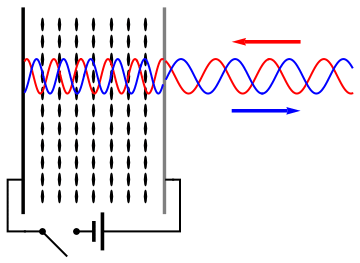
A spatial light modulator (SLM) is a device that can control the intensity, phase, or polarization of light in a spatially varying manner. A simple example is an overhead projector transparency. Usually when the term SLM is used, it means that the transparency can be controlled by a computer.

SLMs are primarily marketed for image projection, displays devices,[1] and maskless lithography.[citation needed] SLMs are also used in optical computing and holographic optical tweezers.

Usually, an SLM modulates the intensity of the light beam. However, it is also possible to produce devices that modulate the phase of the beam or both the intensity and the phase simultaneously. It is also possible to produce devices that modulate the polarization of the beam, and modulate the polarization, phase, and intensity simultaneously.[2]

SLMs are used extensively in holographic data storage setups to encode information into a laser beam similarly to the way a transparency does for an overhead projector. They can also be used as part of a holographic display technology.

In the 1980s, large SLMs were placed on overhead projectors to project computer monitor contents to the screen. Since then, more modern projectors have been developed where the SLM is built inside the projector. These are commonly used in meetings for presentations.

Liquid crystal SLMs can help solve problems related to laser microparticle manipulation. In this case spiral beam parameters can be changed dynamically.[3]

Electrically-addressed spatial light modulator (EASLM)

[edit]

As its name implies, the image on an electrically addressed spatial light modulator is created and changed electronically, as in most electronic displays. EASLMs usually receive input via a conventional interface such as VGA or DVI input. They are available at resolutions up to QXGA (2048 × 1536). Unlike ordinary displays, they are usually much smaller (having an active area of about 2 cm²) as they are not normally meant to be viewed directly. An example of an EASLM is the digital micromirror device (DMD) at the heart of DLP displays or LCoS Displays using ferroelectric liquid crystals (FLCoS) or nematic liquid crystals (electrically controlled birefringence effect).

Spatial light modulators can be either reflective or transmissive depending on their design and purpose.[4]

DMDs, short for digital micromirror devices, are spatial light modulators that specifically work with binary amplitude-only modulation.[5][6] Each pixel on the SLM can only be in one of two states: "on" or "off". The main purpose of the SLM is to control and adjust the amplitude of the light.

Phase modulation can be achieved using a DMD by using Lee holography techniques, or by using the superpixel method.[7][6]

Optically-addressed spatial light modulator (OASLM)

[edit]

The image on an optically addressed spatial light modulator, also known as a light valve, is created and changed by shining light encoded with an image on its front or back surface. A photosensor allows the OASLM to sense the brightness of each pixel and replicate the image using liquid crystals. As long as the OASLM is powered, the image is retained even after the light is extinguished. An electrical signal is used to clear the whole OASLM at once.

They are often used as the second stage of a very-high-resolution display, such as one for a computer-generated holographic display. In a process called active tiling, images displayed on an EASLM are sequentially transferred to different parts on an OASLM, before the whole image on the OASLM is presented to the viewer. As EASLMs can run as fast as 2500 frames per second, it is possible to tile around 100 copies of the image on the EASLM onto an OASLM while still displaying full-motion video on the OASLM. This potentially gives images with resolutions of above 100 megapixels.

Application in ultrafast pulse measuring and shaping

[edit]

Multiphoton intrapulse interference phase scan (MIIPS) is a technique based on the computer-controlled phase scan of a linear-array spatial light modulator. Through the phase scan to an ultrashort pulse, MIIPS can not only characterize but also manipulate the ultrashort pulse to get the needed pulse shape at target spot (such as transform-limited pulse for optimized peak power, and other specific pulse shapes). This technique features with full calibration and control of the ultrashort pulse, with no moving parts, and simple optical setup. Linear array SLMs that use nematic liquid crystal elements are available that can modulate amplitude, phase, or both simultaneously.[8][9]

See also

[edit]

References

[edit]
[edit]
Revisions and contributorsEdit on WikipediaRead on Wikipedia
from Grokipedia
A spatial light modulator (SLM) is an optical device that modulates the , phase, polarization, or a combination thereof of waves in a spatially and temporally varying manner across its surface. These devices typically feature a two-dimensional array of independently addressable pixels—often numbering in the millions—that enable precise control over incident beams, transforming static optical elements into dynamic, programmable tools for manipulation. SLMs can be broadly categorized by their addressing mechanism and optical architecture: electrically addressed SLMs respond to electrical signals for pixel control, while optically addressed variants use incident patterns; additionally, they operate in transmissive mode (light passes through) or reflective mode (light bounces off). Dominant technologies include (LCOS) SLMs, which exploit the electrically induced of liquid crystals to achieve high-resolution by altering the and within each pixel. Other implementations leverage micro-electro-mechanical systems (), such as deformable mirror arrays, for rapid surface profile adjustments that impart wavefront aberrations or corrections. The versatility of SLMs has driven their adoption across diverse fields, including for real-time 3D imaging and displays, in astronomy and to compensate for atmospheric distortions, and structured light generation for applications in , processing, and high-speed . Recent advances emphasize higher pixel densities (e.g., beyond ), faster refresh rates, and operation to support emerging needs in , laser processing, and biomedical imaging.

Overview

Definition and Basic Principles

A spatial light modulator (SLM) is an optical device that modulates the , phase, polarization, or a combination of these properties of an incident wave in a spatially varying manner across its . These devices function as programmable optical elements, enabling pixel-by-pixel control of wavefronts to shape or redirect beams dynamically. SLMs typically offer resolutions ranging from 10^5 to 10^7 , with pixel sizes on the order of 5-20 μm, allowing for fine spatial control comparable to digital displays but optimized for coherent manipulation. Key performance parameters include the fill factor, defined as the ratio of the active area to the total pixel area (ideally exceeding 90% to minimize losses), modulation depth (such as a phase shift from 0 to 2π radians for full wavefront control), response time (often in the range for common implementations), and efficiency (typically 70-90%, influenced by pixel geometry and material losses). These parameters determine the device's ability to perform high-fidelity optical transformations without significant unwanted or . At their core, SLMs rely on wavefront modulation principles rooted in , where the device is often placed in the Fourier plane of an optical system to impose a spatially varying phase or pattern on the light field. This enables the synthesis of complex beam profiles, such as focusing or steering, by altering the across the aperture. The φ(x,y) at position (x,y) is fundamentally given by ϕ(x,y)=2πλΔn(x,y)d,\phi(x,y) = \frac{2\pi}{\lambda} \Delta n(x,y) \, d, where λ is the of the , Δn(x,y) is the spatially varying change in , and d is the interaction thickness of the modulating medium. SLMs can be addressed electrically or optically to achieve this control, though detailed mechanisms vary by design.

Historical Development

The conceptual foundations of spatial light modulators (SLMs) emerged in the amid proposals for , spurred by the invention of the in 1960, which highlighted the need for devices capable of real-time spatial modulation of for applications. Early efforts focused on overcoming limitations of static optical elements like photographic slides, leading to initial explorations of dynamic modulators. Practical SLMs appeared in the , with acousto-optic devices enabling one-dimensional modulation through sound wave-induced of , commonly integrated into optical correlators and analyzers. Magneto-optic effects were also harnessed in early spatial modulators, such as those using Faraday for polarization control in two-dimensional arrays, marking the transition toward more versatile manipulation. Notable milestones included the development of the first SLM in the late 1960s as a 2 × 18 matrix device, followed by an optically addressed valve (LCLV) by Hughes Corporation in 1978, which achieved a resolution of about 40 line pairs per millimeter and operated at video rates despite its bulkiness. The 1980s and 1990s saw explosive growth, with over 50 SLM variants introduced to meet demands in optical information processing and , largely driven by U.S. military research funded by for applications in beam control and through atmospheric . Key innovations included liquid crystal-based SLMs, with advancing deformable mirror technologies as precursors to the (DMD), patented in 1987 and initially explored for coherent optical processing. In the 2000s, the focus shifted to liquid crystal on silicon (LCOS) SLMs, which offered higher resolution through silicon backplanes with finer pixel pitches, facilitating broader commercialization in digital displays and emerging holography systems. This era's market expansion was closely linked to digital projection technologies, exemplified by Texas Instruments' DLP systems, which debuted commercially in the late 1990s and dominated cinema and home theater applications by the mid-2000s. The 2010s and 2020s witnessed accelerated LC SLM progress through integration with , enabling ultrafast operation and compact designs. Significant advancements included high-refresh-rate SLMs reaching 144 Hz frame rates by 2018 for dynamic , and phase-only LCOS modulators surpassing (e.g., 3840 × 2160 pixels) by 2020, supporting applications in high-fidelity shaping. By 2025, resolutions have reached up to 10 megapixels (e.g., 4160 × 2464 pixels) in devices like the HOLOEYE GAEA-2.1, with some models supporting over 1 kW power for industrial applications. Throughout this progression, SLM technology evolved from analog mechanisms, reliant on continuous physical effects like reorientation, to digital addressing via pixelated arrays, propelled by Moore's Law-driven advances in VLSI fabrication and the imperative for precise, real-time control in adaptive systems.

Types

Electrically Addressed SLMs

Electrically addressed spatial modulators (SLMs) operate by applying electrical signals to an of pixels, each capable of independently modulating the properties of incident , such as phase, , or polarization. These devices integrate seamlessly with electronic control systems, enabling real-time reconfiguration through digital inputs. The core architecture typically consists of a pixelated backed by a substrate that facilitates precise electrical addressing, distinguishing them from other SLM variants by their direct compatibility with standard computing interfaces. The addressing mechanism relies on electrical signals delivered to individual pixel electrodes, which alter the of the active material within each . For instance, voltage gradients are applied row-by-row or via (TFT) arrays to control molecular alignment or mechanical deflection, with inputs commonly sourced from video signals or computer interfaces such as VGA or ports. This allows for dynamic pattern loading at frame rates up to several hundred hertz, supporting applications requiring rapid updates. Among the primary technologies, liquid crystal on silicon (LCOS) devices utilize a reflective silicon backplane coated with a liquid crystal layer, enabling both phase and amplitude modulation through electro-optic effects in nematic or ferroelectric liquid crystals. LCOS SLMs achieve continuous gray-scale control via analog voltage addressing or pulse-width modulation (PWM) in digital modes, with vertical alignment (VA) or twisted nematic (TN) configurations optimizing performance across visible to near-infrared wavelengths. In contrast, the digital micromirror device (DMD) employs micro-electro-mechanical systems (MEMS) where each pixel is a tiltable aluminum mirror array, providing binary amplitude modulation by directing light toward or away from the output path. Developed by Texas Instruments, DMDs use electrostatic actuation to switch mirrors, with grayscale achieved through PWM at high frequencies. Key characteristics of electrically addressed SLMs include response times ranging from 1 to 30 ms, influenced by the reorientation speed in LCOS or the mechanical settling in DMDs, allowing for video-rate operation in many setups. Resolutions extend up to 8K (e.g., 7680 × 4320 ) in advanced LCOS models, with pixel pitches as small as 3 μm, while DMDs commonly offer to 4K arrays with micromirror pitches around 5-10 μm. Power is enhanced by backplanes in LCOS, which minimize drive voltages, and DMDs benefit from low-power actuation. For DMDs, the modulation arises from mirror tilting, where the output intensity follows Icos2(θ)I \propto \cos^2(\theta), with θ\theta typically ±12° to optimize into the desired order. These SLMs offer advantages such as high integration with electronics, enabling compact designs and straightforward interfacing with standard hardware, as exemplified by ' DLP chips introduced in for projection systems. However, limitations include susceptibility to charge trapping in LCOS devices, which can cause retention and requires periodic field inversion to maintain uniformity, potentially reducing effective frame rates. DMDs, while robust, are constrained to natively, necessitating PWM for analog-like control, which may introduce temporal artifacts at high speeds.

Optically Addressed SLMs

Optically addressed spatial light modulators (OASLMs) operate by using an incident write beam, typically in the UV or visible spectrum, to induce spatial patterns of charge separation or refractive index variation within a photosensitive layer, which then modulates a separate probe beam for readout. This mechanism relies on photoexcitation creating free carriers that migrate under diffusion or an applied field, forming a space-charge distribution that alters the material's optical properties via the electro-optic effect. The resulting modulation can achieve both amplitude and phase control, enabling applications in real-time image processing. Primary technologies for OASLMs include photorefractive devices based on inorganic crystals such as bismuth silicon oxide (BSO) and (LiNbO₃), which exploit volume holographic recording for high-fidelity pattern transfer. In BSO-based systems like the (PROM), the write beam records interference gratings directly in the crystal, allowing recyclable operation without mechanical erasure. LiNbO₃ variants, often doped for enhanced sensitivity, support similar photorefractive recording but with improved thermal stability. Hybrid OASLMs incorporate a photoconductive layer, such as or , paired with an electro-optic layer like or ferroelectric material, to accelerate carrier generation and separation for faster response times compared to pure photorefractive setups. Key characteristics of these OASLMs include optical gain exceeding unity, enabling signal amplification through two-beam , with resolutions reaching approximately 1000 lines per millimeter in optimized photorefractive crystals. Response times typically range from 10 to 100 milliseconds, influenced by resistivity and illumination intensity, allowing video-rate operation in hybrid configurations. The photorefractive index modulation is governed by the relation ΔnEscL\Delta n \propto E_{sc} \cdot L, where EscE_{sc} is the space-charge field and LL is the period, highlighting the dependence on charge separation efficiency and spatial frequency. These devices offer advantages such as exceptional sensitivity to low-intensity write beams (down to microwatts per square centimeter) and inherent optical gain for noise suppression in coherent systems. However, they are limited by the need for coherent or partially coherent write illumination to form stable gratings and slower erasure compared to electrically addressed counterparts, restricting throughput in high-speed scenarios. Historically, OASLMs found prominent use in 1980s optical correlators for real-time and Fourier processing tasks.

Other Types

Other electrically addressed SLMs include deformable mirror devices, which consist of arrays utilizing electrostatic actuators to enable phase-only correction through surface deformation. These devices typically operate in or tip-tilt modes, where individual mirror segments move vertically () or angularly (tip-tilt) to adjust lengths. Actuator strokes reach up to 5 μm, providing sufficient range for correcting low-order aberrations in systems. Acousto-optic SLMs leverage sound waves propagating through a transparent medium to induce gratings, thereby modulating via . These devices, such as acousto-optic deflectors, achieve high modulation speeds with bandwidths exceeding 1 GHz, enabling rapid and scanning. Magneto-optic SLMs, in contrast, employ magnetic fields to alter the polarization or phase of through the Faraday or Kerr effects in magnetophotonic materials. Emerging hybrid SLMs incorporate ferroelectric liquid crystal (FLC) layers for enhanced performance, achieving switching times below 1 ms due to the bistable nature of FLC molecules under electric fields. Key specifications for acousto-optic hybrids include diffraction angles governed by the Bragg condition: sinθB=λ2Λ\sin \theta_B = \frac{\lambda}{2 \Lambda} where λ\lambda is the optical wavelength and Λ\Lambda is the acoustic period. These other types of SLMs are primarily suited to niche applications requiring high-speed operation or large apertures, such as ultrafast processing or astronomical , with commercial examples including Micromachines' deformable mirrors developed since the early 2000s.

Operating Principles

Modulation Mechanisms

Spatial light modulators (SLMs) achieve primarily through pixel-level absorption or of light, altering the intensity without significantly affecting the phase. A common implementation uses twisted nematic (TNLC) layers, where an electric field rotates the molecular director by up to 90 degrees, changing the polarization state of transmitted light and blocking or allowing passage through an analyzer . This rotation modulates transmission from near 0% to nearly 100%, yielding high ratios exceeding 1000:1 for precise on-off control in applications like binary . Phase modulation in SLMs relies on spatially varying the refractive index or optical path length to impart a controlled phase delay across the wavefront. In liquid crystal on silicon (LCOS) devices, an applied voltage tilts the nematic director, inducing birefringence changes that depend on the field strength; the effective birefringence is approximated as Δn=Δnmaxsin2α\Delta n = \Delta n_{\max} \sin^2 \alpha, where α\alpha relates to the director orientation under the electric field. The resulting phase shift for a reflective configuration is Γ=4πdΔnλ\Gamma = \frac{4\pi d \Delta n}{\lambda}, with dd as the liquid crystal layer thickness and λ\lambda the wavelength, enabling up to 2π2\pi retardation for wavefront shaping. Polarization modulation provides vectorial control over the light's orientation, leveraging the anisotropic properties of materials like nematic liquid crystals to rotate or retard specific polarization components. In advanced SLMs, this is achieved by configuring the device to act as a tunable retarder or rotator , often using homogeneous or twisted alignments that respond to voltage by altering the fast and slow axes. When combined with , such systems enable manipulation of all four (S0,S1,S2,S3S_0, S_1, S_2, S_3), allowing arbitrary polarization states to be synthesized across the beam for applications in vector beam generation. Multi-parameter SLMs extend functionality by enabling simultaneous and phase control, addressing limitations of single-parameter devices through cascaded or dual-layer architectures. In dual-layer designs, one layer modulates phase via while the second handles through polarization-dependent absorption, achieving complex field encoding in the target order. For phase-only SLMs approximating , a periodic phase pattern diffracts into orders, with the zeroth-order transmission given by T0=[J0(ϕ)]2T_0 = [J_0(\phi)]^2, where ϕ\phi is the peak phase depth and J0J_0 the zeroth-order of the first kind; optimizing ϕ2.405\phi \approx 2.405 (a zero of J0J_0) suppresses the undiffracted beam, directing over 90% of energy to higher orders for effective intensity control.

Materials and Technologies

materials form the basis of many spatial light modulators, particularly in electrically addressed configurations, where their enables phase or polarization modulation. Nematic s are widely employed due to their high , typically on the order of Δn ≈ 0.2, which supports efficient phase shifts but is limited by slower response times on the scale. In contrast, ferroelectric s provide faster switching speeds in the range, albeit with somewhat lower around Δn ≈ 0.1, making them suitable for dynamic applications requiring rapid reconfiguration. To achieve uniform molecular orientation, known as director control, alignment layers—such as rubbed or photoaligned polymers—are applied to the substrate surfaces, ensuring consistent pretilt angles and minimizing defects that could degrade modulation uniformity. Silicon backplanes are essential for (LCOS) devices, leveraging (CMOS) technology to drive pixel arrays with high precision. These backplanes achieve fill factors exceeding 90% by minimizing inactive areas around reflective electrodes, thereby maximizing optical efficiency and reducing losses. Fabrication employs very-large-scale integration (VLSI) processes, including and metal deposition, to create dense arrays with pixel pitches below 10 μm, enabling high-resolution modulation for applications demanding fine spatial control. Photorefractive materials underpin optically addressed spatial light modulators (OASLMs), where light-induced charge redistribution creates gratings. Inorganic crystals like bismuth silicon oxide (BSO) are favored for their and sensitivity, allowing efficient recording of holograms at low intensities. Organic polymers, such as those doped with nonlinear chromophores like 2,4,7-trinitro-9-fluorenone (TNF), offer advantages in flexibility and ease of processing for OASLM fabrication, though they generally exhibit lower sensitivity compared to inorganics but benefit from tunable electro-optic coefficients. Micro-electro-mechanical systems () in digital micromirror devices (DMDs) utilize aluminum mirrors suspended on torsion hinges to enable binary through tilting. These structures are fabricated using , involving sequential deposition and etching of aluminum layers to form the mirrors, hinges, and yokes, with defining precise features down to micrometer scales. Effective thermal management is critical for high-power operation, as DMDs can handle incident intensities exceeding 1 kW/cm² in pulsed modes, achieved through heat sinking and material choices that dissipate absorbed energy without deforming the delicate hinges.

Applications

Ultrafast Optics

Spatial light modulators (SLMs) play a crucial role in ultrafast by enabling precise control over the temporal and properties of short pulses, typically in the to regime. These devices, particularly liquid crystal-based SLMs, allow for programmable across the spectrum, facilitating both characterization and manipulation of ultrashort pulses. This capability has been foundational since the , when early demonstrations integrated SLMs into shapers to achieve dynamic synthesis. In pulse measurement, SLMs enhance techniques like () by incorporating iterative algorithms. In setups, an SLM can introduce known phase perturbations to the replicas, aiding the reconstruction of intensity and phase from the trace through generalized projections or principal component generalized projections algorithms. This SLM-assisted approach improves accuracy for complex , as demonstrated in experiments where SLM-shaped waveforms were characterized via combined and cross-correlation () traces. Similarly, spectral phase interferometry for direct electric-field reconstruction () benefits from SLM calibration, where the modulator applies reference phases to verify and correct spectral distortions in real-time, enabling self-referenced measurements of and higher-order dispersion. For , SLMs operate in a Fourier-domain configuration, commonly using a 4f zero-dispersion shaper setup that disperses the via a and lens pair, modulates the phase pixel-by-pixel on the SLM, and recombines the components. Pixelated phase masks on the SLM allow for tailored spectral phase profiles to compress ; for instance, a linear compensation introduces a quadratic phase φ(ω) = \frac{1}{2} \text{GDD} (\omega - \omega_0)^2 that counters the input dispersion, where \text{GDD} = \frac{d^2 \phi}{d \omega^2} is the group delay dispersion applied by the SLM. This enables near-transform-limited output, as shown in experiments compressing to 5 fs durations using solely SLM phase control without additional . The key benefits of SLM-based control include achieving sub-10 fs pulse durations essential for attosecond science, where shaped pulses drive high-harmonic generation and electron dynamics in atoms. In multiphoton , SLMs optimize pulse shapes to enhance nonlinear signals like , improving resolution and contrast. Coherent control applications, pioneered in the , leverage SLM shaping to selectively excite molecular pathways, such as in selective bond dissociation or preparation. Despite these advantages, SLMs face limitations in bandwidth, typically constrained to around 100 THz for visible wavelengths due to the finite pixel resolution and response time, which restricts handling of ultrabroadband spectra beyond the near-infrared.

Holography and Beam Shaping

Spatial light modulators (SLMs) play a pivotal role in by serving as displays for computer-generated holograms (CGHs), enabling the precise reconstruction of complex optical fields. In this context, SLMs modulate the phase of an incident to encode holographic , allowing for the generation of three-dimensional images or arbitrary patterns without physical recording media. A key computational method for creating these phase-only CGHs is the Gerchberg-Saxton (GS) algorithm, which iteratively retrieves the phase distribution from intensity constraints in both the object and Fourier planes, optimizing the hologram for high fidelity reconstruction. This approach, originally proposed in 1972, has become foundational for SLM-based due to its efficiency in handling problems. Beam shaping with SLMs extends this capability to engineer arbitrary intensity and phase profiles, such as non-diffracting s or arrays of focused spots, which maintain their structure over propagation distances. These profiles are achieved by designing CGHs that impose specific phase patterns on the SLM, often incorporating blazed gratings to direct into desired orders while minimizing losses to zeroth-order or unwanted modes. Blazed gratings optimize by approximating a sawtooth phase profile that matches the , enabling efficient redirection of . For instance, SLMs can generate arrays for applications requiring extended focal lines, or multi-foci arrays for parallel processing in optical systems. In practical applications, SLMs facilitate correction in systems for astronomical telescopes, where they dynamically compensate for atmospheric distortions to sharpen stellar images. By applying corrective phase patterns derived from sensors, SLMs restore the planarity of incoming , enhancing resolution in large-aperture observatories. Similarly, in optical trapping, SLMs generate multiple configurable traps through holographic techniques, allowing simultaneous manipulation of microscopic particles in three dimensions for studies in and physics. The reconstructed holographic field U(x,y)U(x,y) at the observation plane under the Fresnel approximation is given by U(x,y)=SLM(ξ,η)exp[ik(rξxrηyr)]dξdη,U(x,y) = \int \text{SLM}(\xi,\eta) \exp\left[i k \left(r - \frac{\xi x}{r} - \frac{\eta y}{r}\right)\right] d\xi \, d\eta, where k=2π/λk = 2\pi / \lambda is the wavenumber, rr is the propagation distance, and the integral approximates the diffracted field from the SLM plane. Electrical addressing enables real-time updates to these CGHs, supporting dynamic control in such systems. Phase-only holograms implemented on SLMs can achieve diffraction efficiencies exceeding 90%, particularly with optimized blazed grating designs and high-quality liquid crystal layers.

Displays and Projection

Spatial light modulators (SLMs) play a pivotal role in modern projection systems, particularly through digital light processing (DLP) technology utilizing digital micromirror devices (DMDs). In cinema applications, three-DMD configurations achieve full-on/full-off contrast ratios exceeding 1000:1, enabling film-quality images with high brightness and over 14 bits of per color. These systems support binary frame rates up to 9700 Hz for efficient light modulation, facilitating smooth playback at standard cinema refresh rates around 120 Hz while maintaining superior image uniformity and efficiency near 65%. Liquid crystal on silicon (LCOS) SLMs complement DMDs in high-brightness projectors, offering advantages in resolution and light throughput due to their constant aperture ratios approaching 93% and vertically aligned liquid crystals for faster response times. For instance, WUXGA LCOS panels (1920 × 1200 pixels, 9.5 μm pitch) deliver high contrast optimized for green wavelengths around 535 nm, supporting brighter projections without sacrificing detail in demanding environments like large-venue displays. Sequential contrast ratios in advanced LCOS variants reach 800:1 to 1400:1, enhancing black levels and color fidelity in reflective architectures. In head-mounted displays, SLMs enable compact micro-projectors for (AR) glasses by modulating coherent light directly, as seen in phase-only LCOS designs (e.g., 1080 × 1920 pixels, 6.4 μm pitch) paired with lensless holographic engines. This integration minimizes device thickness by mounting the SLM near in-coupling gratings, supporting full-color 3D imagery with see-through efficiencies up to 78.4% across RGB wavelengths (445 nm , 521 nm , 638 nm ). Holographic optical elements (HOEs), such as metasurface waveguides or volume gratings, expand the field of view (FOV) beyond 60°, achieving up to 80° diagonal in see-through near-eye systems while expanding the eye-box to 7.5 mm horizontally for comfortable viewing. Color reproduction in SLM-based displays relies on RGB modulation via sequential or spatial methods, where LCOS panels sequentially illuminate red, green, and blue channels to synthesize full-color images without color wheels, reducing artifacts and enabling high-frame-rate operation up to 24 fps in holographic setups. Spatial approaches, using multi-layer or off-axis configurations, support complex amplitude and phase modulation for vibrant holograms on single 4K SLMs (e.g., 4160 × 2464 pixels, 3.74 μm pitch), delivering resolutions suitable for immersive projection. These panels achieve wide viewing angles exceeding 60° through diffractive HOEs, maintaining uniformity across the visible spectrum. SLM technologies have dominated digital projectors since the early 2000s, with one-chip DLP systems capturing over 60% of the DLP projector market by 2024, driving adoption in home entertainment and cinema. Portable units, leveraging efficient DMD or LCOS designs, consume 50–100 watts, balancing high lumen output with battery-powered mobility for consumer applications.

Advanced Manufacturing and Sensing

Spatial light modulators (SLMs) serve as dynamic masks in maskless lithography systems, enabling direct patterning without physical photomasks for both deep ultraviolet (DUV) and extreme ultraviolet (EUV) wavelengths. This approach utilizes pixel-parallel exposure, where the SLM modulates light to project intricate patterns onto photoresist-coated substrates, significantly reducing mask fabrication costs and turnaround times compared to traditional methods. For instance, micro-electro-mechanical systems (MEMS)-based SLMs have been developed to achieve continuous vertical motion of 80 nm for DUV modulation, supporting high-resolution patterning in semiconductor manufacturing. In EUV maskless lithography, SLMs address the high expense of conventional masks, which can exceed $120,000 per unit, by enabling on-the-fly pattern generation for applications requiring multiple mask variants. In laser processing, SLMs facilitate beam homogenization and multi-spot generation, enhancing efficiency in industrial applications such as , cutting, and . By reshaping beams into uniform profiles or multiple foci, SLMs improve energy distribution, reducing thermal distortions and enabling parallel processing that accelerates throughput in metal via laser powder bed fusion (LPBF). For example, (LCoS) SLMs divide a single beam into multiple spots for efficient , as demonstrated in bio-inspired surface fabrication where seven-beam patterns were used to process materials like . Beam shaping via SLMs also supports spatially oscillating LPBF, where dynamic modulation captures melt pool dynamics to optimize in-situ imaging and spatter control. SLMs play a crucial role in sensing and through and interferometric techniques, providing real-time aberration correction and feedback for precision measurements. In , SLMs correct depth-induced spherical aberrations by modulating , enabling clearer in deep tissue samples without relying on fluorescent references. This is achieved via closed-loop systems where the SLM compensates for distortions using wavefront sensing, as seen in ophthalmic applications where a single SLM handles both sensing and correction. For , interferometric feedback with SLMs calibrates in parallel-aligned devices, using auto-referenced Michelson interferometers to quantify and compensate for surface deformations with sub-wavelength accuracy. Integration of SLMs in metal systems exemplifies their industrial impact, with devices like the Santec SLM-310 designed for high-power lasers in welding and LPBF processes, featuring for sustained operation. Seurat Technologies employs optically addressed SLMs (OASLM) for beam shaping in area , simulating effects to achieve rapid, high-resolution metal part fabrication. These systems support throughputs exceeding 10^6 patterns per second in maskless configurations, as evidenced by reflective SLM designs that double exposure rates through seamless large-area patterning. Deformable mirrors, akin to SLM variants, further aid in aberration correction for such setups.

Recent Advancements

High-Power and Spectral Extensions

Recent advancements in spatial light modulators (SLMs) have focused on enhancing their power handling capabilities to support applications with high-intensity laser sources. Modified (LC) layers in LCOS-based SLMs have achieved total power handling exceeding 1 kW (CW) at 1070 nm by incorporating robust alignments and dielectric coatings that minimize thermal degradation. Cooling systems, such as integrated water circulation or Peltier elements, further enable sustained operation with industrial lasers exceeding 1 kW at 1070 nm, preventing phase instabilities from heat buildup. These improvements allow SLMs to maintain efficiencies above 90% under prolonged high-power exposure. Spectral extensions have broadened SLM operability into (UV) and (IR) regimes, addressing limitations of traditional visible-range devices. For UV applications below 300 nm, SLMs employing aluminum mirror arrays on MEMS-based pistons, as developed in 2025, provide high-fidelity for applications including atom trapping and precise manipulation of cold atoms. In the IR domain, low-loss polymer-stabilized LC mixtures extend functionality up to 5 μm with absorption losses under 1 dB/cm, supporting mid-wave IR beam shaping in thermal imaging and . Key developments include larger-area LCOS SLMs surpassing 1 inch in active diagonal by 2023, facilitating scalable and wide-field beam control with pixel pitches below 8 μm. Complementary MEMS UV mirror arrays achieve reflectivities over 95% across 200-400 nm, enhancing efficiency in deep-UV and . These innovations stem from optimized fabrication processes that integrate high-reflectivity coatings directly onto deformable microstructures. Despite these advances, challenges persist at high intensities, where nonlinear optical effects such as self-phase modulation and two-photon absorption distort wavefronts, reducing modulation fidelity. Anti-reflective coatings on SLM surfaces mitigate these issues by suppressing unwanted reflections and laser-induced damage thresholds, achieving up to 50% improvement in peak power tolerance. Ongoing research emphasizes multilayer dielectric designs to balance broadband performance with thermal management.

Integration and Future Prospects

Spatial light modulators (SLMs) are increasingly integrated with (AI) algorithms to enable real-time optimization in dynamic optical systems, particularly in where feedback loops adjust phase patterns for enhanced image fidelity. For instance, models process distortions and iteratively refine SLM configurations, achieving sub-millisecond corrections in holographic displays. This synergy extends to hybrid architectures combining SLMs with photonic integrated circuits, allowing compact modules for on-chip shaping in platforms, which reduces system footprint while maintaining high modulation efficiency. The SLM market is projected to grow at a (CAGR) of 13.6% from 2025 to 2032, reaching approximately USD 1.68 billion, primarily driven by demand in (AR)/ (VR) headsets for precise and in for manipulating entangled photon states. Evaluation platforms, such as Fraunhofer IPMS's 2025 kits featuring 256x256 micromirror arrays with integrated control electronics, facilitate and performance testing for these applications. Looking ahead, advancements aim for sub-millisecond response times through graphene-enhanced (LC) layers, which improve conductivity and reduce switching latencies to around 0.7 ms in metasurface configurations, enabling ultrafast modulation for high-frame-rate systems. Key challenges include high production costs, currently limiting accessibility, with ongoing efforts targeting reductions below $1000 per unit through scalable fabrication techniques. In emerging applications, SLMs enhance 3D by generating structured light patterns for precise surface profiling and defect detection in optical systems. For bio-imaging, SLM-based correction enables high-throughput, diffraction-limited imaging of cellular structures, while SLM-driven printing of custom supports tailored microlens arrays for .

References

Add your contribution
Related Hubs
User Avatar
No comments yet.