

Community hub
Recent from talks
Contribute something
Nothing was collected or created yet.
TMS9918
View on WikipediaThis article needs additional citations for verification. (April 2015) |
 TMS9918A VDP | |
| Component type | video display controller |
|---|---|
| First produced | 1979 |
The TMS9918 is a video display controller (VDC) manufactured by Texas Instruments and introduced in 1979.[1] In TI's manuals it's called a "Video Display Processor" (VDP). The TMS9918 and its variants are used in the Casio PV-2000, Coleco Adam, ColecoVision, CreatiVision, Hanimex Pencil II, MSX, Memotech MTX, NABU Personal Computer, PECOS, SG-1000, SC-3000, SV-318, SV-328, Sord M5, TI-99/4, Tatung Einstein, and Tomy Tutor.
The TMS9918 was an advanced design for the era. It had four graphics modes based on an underlying 256 wide by 192 high pixel layout, which could be used as a 40 by 24 character display, a 256 by 192 pixel display, or a 64 by 48 pixel display which used less memory. It had a fixed color palette with 15 colors plus transparent. It also supported 32 single-color 8x8 or 16x16 pixel sprites, numbered 0 to 31, with lower-numbered sprites appearing on top of higher-numbered ones. This allowed for layering and perspective effects. It also featured a video input and sync pin, which allowed video from another source to appear under the graphics being created by the chip. This could be used to layer the output from multiple 9918's, or to use the 9918 as a system for titling and overlays on other video sources.
To support this advanced feature set, the 9918 required fast access to memory. To allow this, it was given a dedicated 16 KB pool of RAM that was separate from the main memory of the computer that it was part of. TI referred to this as VRAM. This meant that the CPU could only update the video display over a separate 8-bit data bus with the VDP moving data on the bus to and from its dedicated RAM. This limited the speed at which the CPU and 9918 could communicate. It also meant that the common solution of using the video chip to refresh memory could not be used and had to be implemented in separate hardware. While these represented minor complications compared to systems that shared memory in a single pool, the result was a display that was much more colorful and offered some parity with arcade game-level displays.
The Yamaha V9938 is an enhanced version of the TMS9918.
Description
[edit]General information
[edit]

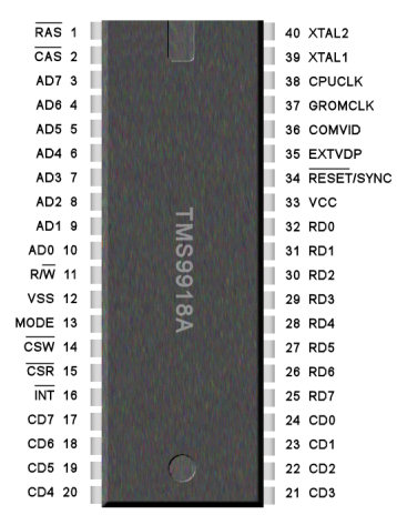
The TMS9918 was packaged in a 40-pin dual in-line package (DIP). Power was provided as +5V on pin 33, VCC, and ground on pin 12, VSS. A quartz crystal running at 10.7386 MHz, three times the NTSC colorburst frequency, was connected across pins 40, XT1, and 39, XT2. Video output was on pin 36, COMVID, and input, if used, on pin 35, EXTV, with their connector's shield connection connected to ground.[3]
In order to achieve the memory performance needed to support full-color operation, the system used a dedicated area of DRAM they referred to as VRAM. To operate this memory, the system included a separate set of pins forming an 8-bit address bus on pins 3 (AD7) through 10 (AD0) and an 8-bit data bus on pins 25 (RD7) through 32 (RD0), supported by a read/write control on pin 11, and RAS and CAS on pins 1 and 2.[3]
Communications with the host computer were through a separate 8-bit data bus on pins 17 through 24, D7 to D0. Pin 13, MODE, controls whether the data on that bus is an address or data. To write to the TMS9918, the CPU first sets the mode and writes data to an internal address register, then writes the data to the bus and changes the mode to cause the data to be deposited into that address. After the data byte is read, the TMS9918 increments the pointer in the address register, allowing a series of bytes to be written in succession.[4]
The TMS9918 logically arranges graphics in a number of layers, 32 sprite layers on top, a graphics or text layer, a "backdrop" with a single solid color filling the screen, and finally an external video layer. The backdrop plane is slightly larger than the others, so it completely fills the screen. The system uses a 15-color palette, along with color 0 which is transparent. At any pixel location on the screen, the system sees if a particular object is in that location, and whether or not it is set to transparent. If it is transparent it looks at the next object, and so on, until it reaches the external video layer (which is often not used).[5] The following descriptions are ordered in this same fashion.
Sprites
[edit]A key feature of the 9918 series was its powerful sprite support. It used a series of 8 bytes in VRAM to store patterns for 8 by 8 pixel sprites, one byte for each line of 8 pixels. It also had a second mode with 16 by 16 pixel sprites, 2 bytes per row and 16 rows.[6] Additionally, either size of sprite could be magnified two times to make the spites larger on the screen. The pattern data for the sprites, in 8 or 32 byte long entries, was held in a block of memory known as the sprite generator table (SGT).[7]
In addition to the 8 or 32 byte long entries holding the patterns, there was a separate sprite attribute table (SAT) that defined how the data was interpreted and displayed. This included 8-bit values for the horizontal and vertical position of the sprite, a pointer to the start of the data for that sprite in the SGT (which they called the name), and a color code in the lower four bits, for a total of 4 bytes per sprite for a total of 128 bytes in the SAT.[6]
To determine what color to display at any given pixel on the screen, the system looked to see which sprites were visible at that location, and then searched down the patterns until it found the first one that held a 1 in that location, then drew the color found in the SAT at that pixel. This caused the sprites to be displayed in order, such that lower numbered sprites appeared on top of higher numbered ones. That meant, for instance, that sprite 0 always appeared on top. If there was no sprite on the screen at that location with a 1, that pixel was transparent, and the background graphics would be displayed instead.[8]
As the sprites were drawn in order, it is sometimes necessary to change that order to produce the desired layering effects. This is the purpose of the "name" field entries in the SAT. For instance, if one wants to change the display so sprite 10 appears in front of 5, the values in the name field entries of the two can be swapped, avoiding the need to move the pattern data. Through careful arrangement of the sprite ordering, the system can easily produce pseudo-3D and parallax scrolling effects.[9]
Due to performance issues, only four sprites can be displayed on any one scan line. If more are specified on a given line, they will simply not be displayed. The VDP has a status register that reports the number of the first sprite that had to be dropped. It is up to the programmer to design their system to ensure this limit is not reached. One trick to emulate more sprites on a line can be achieved by changing the priorities by swapping the name values every other frame so that one set of four is displayed on one frame and then another on the next. This allows up to eight sprites on a line, but results in noticeable flickering.
The sprite collision flag is set when non-zero pattern bits of two sprites coincide, even if either sprite has transparent colour. The VDP does not indicate which sprites have collided, simply that at least two have done so. This is normally used to trigger more advanced collision detection routines inside the software, which can then determine the exact location of the collision and act upon it.
Graphics modes
[edit]The graphics of the 9918 were based on an underlying 256 wide by 192 high pixel layout.[5] These numbers are typical for systems of the era which used analog video signals for output in a progressive scan display. This is close to the maximum resolution achieved on television sets of the era, which was around 320 by 240, due to the complexity of the NTSC radio-frequency signals.[a]
There were four ways the graphics layer could be used:
Mode 0, or Text Mode, broke the screen into a 40 by 24 layout of "blocks", each 6 pixels wide and 8 high. Each block could hold a value from 0 to 255, normally representing an expanded ASCII character set. The patterns for each of the 256 characters was stored in VRAM and could be changed by loading the VRAM values using the CPU. Each line of the characters was defined as a series of "on" or "off" pixels stored in one byte per line, and 8 bytes per character. Because the blocks were 6 by 8 on the screen, it was up to the designer to lay out the characters in a 5 by 7 grid to leave space between them. The color for the "on" and "off" bits in the patterns could be any of the 15 colors available, and stored in VRAM.[3]
Mode 1, or Graphics I, was essentially a modification of Text Mode that broke the screen into a 32 by 24 layout, so that each block was 8 by 8 pixels instead of 6 by 8. The pattern for any given pixel on the screen was looked up from the same 256-entry table of bit patterns as the one holding characters in Text Mode. As there were 768 possible locations and only 256 possible patterns, this mode was limited in the sorts of displays it could produce. Graphics I also added a separate section of VRAM that held the color values for the on and off pixels for any given block, with 768 entries. This meant every block of 8 by 8 pixels could have its own two colors, but the pixels within any block all had to be the same.[7] This is not an uncommon solution for the era, and leads to a well-known problem known as attribute clash when it is not possible to choose colors that to not result in the edges of the cells being visible.
Mode 2, or Graphics II, was a further modification of Graphics I, allowing separate patterns for all 768 blocks, as well as separate color settings for each line within the blocks. This meant any block could use all 15 colors, although only two per line. This display allows any image to be drawn and more colors to be displayed, producing a display that is pixel-addressable and suitable for high-resolution drawing of arbitrary images. The cost is that it requires 32 color entries for each of the 192 lines, as well as an extended pattern map with 768 separate entries, increasing the VRAM needed to hold all of the data to about 12 KB.[10]
Mode 3, or Multicolor Mode, broke the screen into 64 by 48 blocks, for a total of 3072 blocks. There were no patterns in this mode, the entire cell was either on or off. There was a color table entry for each block, so every block could select its own color. This produced a low-resolution but high-color display using less than 3 KB of VRAM.[11]
One limitation of the system is that it did not include hardware fine scrolling support, and could only scroll along cell boundaries, normally 8 lines high. Scrolling was accomplished by moving the pattern already stored in VRAM and then adding data for the new line or column, which took some time to perform. Additionally, as all of the graphics modes were essentially character modes with custom characters in each cell, patterns that spanned cells, like lines or circles, had to calculate the pixels for each line of any given cell and upload those values into the character sets.
Screen Mode 2 details
[edit]Technically, mode 2 is a character mode with a colorful character set. The screen is horizontally divided into three 256×64 pixel areas, each of which gets its own character set. By sequentially printing the characters 0 through 255 in all three areas, the program can simulate a graphics mode where each pixel can be set individually. However, the resulting framebuffer is non-linear.
The program can also use three identical character sets, and then deal with the screen like a text mode with a colorful character set. Background patterns and sprites then consist of colorful characters. This was commonly used in games, because only 32×24 bytes would have to be moved to fill and scroll the entire screen.
The challenge of using TMS9918 mode 2 was that every 8×1 pixel area could have only two colors, foreground and background. They could be freely picked out of the 16 color palette, but for each 8×1 area, only two colors could exist. When rendering a straight line diagonally, one easily could exceed the maximum 2 colors per 8×1 area and end up with "color spill".
Undocumented modes
[edit]Texas Instruments originally only documented the four modes listed above. However, the bit that enables mode 2 is actually a modifier bit for the other modes. Enabling it does three things:[12]
- Expands the color table size to hold entries for each cell.
- Divides the screen horizontally into thirds.
- Changes two address bits of the pattern and color tables into mask bits, which controls whether each third of the screen has its own pattern and color table (mode 2) or not (mode 1).
By toggling this bit in code, three additional modes are possible. Note that although genuine TMS9918A chips support these modes, clones and emulators may not.
- Mode 0 (Text) + Mode 2 (Graphic 2): Known as Bitmap Text Mode. This mode allows for two-color bitmap images, with no color table. This saves memory, at the expense of a slightly reduced horizontal resolution (text mode has a horizontal resolution of 240 pixels instead of 256 pixels like the graphic modes do).
- Mode 1 (Graphic 1) + Mode 2 (Graphic 2): Known as Half-Bitmap Mode. Texas Instruments actually documented this "undocumented" screen mode in their manual titled "Video Display Processors Programmers Guide SPPU004".[13] In section 8.4.2, "Playing Games with VRAM Addressing",[13] they discuss how this mode combines the memory savings of mode 1 with the color detail of mode 2. However, as they go on to say this mode limits the number of sprites that can be displayed to 8 instead of 32. Therefore, the term "undocumented" used to describe this mode is a misnomer. However, because this manual was not widely known, this mode is generally considered to be one of the undocumented modes. Generally, the only reason to use this mode over Mode 2 is to reduce memory consumption.
- Mode 3 (Multicolor) + Mode 2 (Graphic 2): Known as Bitmap Multicolor Mode. This mode is more of a novelty, as it offers nothing beyond what the standard Multicolor mode can already do.
External video
[edit]Another key feature of the 9918 series was its ability to read an external video source and pass that signal through to the output assuming all of the objects above it are transparent. This allows the system to produce graphics which could then be overlaid on an analog source like a video camera or videotape. To make sure the two displays line up properly, the clock from the external source needs to be fed in as well, replacing the clock signal that would normally be generated by a quartz crystal. Some system to match the output strength of the input signal to the output also needs to be provided so one signal does not overwhelm the other.[14]
Colors
[edit]The TMS9918 family chips used a composite video palette. Colors were generated based on a combination of luminance and chrominance values for the TMS9918A and Y, and R-Y (Pr) and B-Y (Pb)values are for the TMS9928A/9929A.[15]
Datasheet values
[edit]The TMS9918 has a fixed 16-color palette, composed of 15 displayed colors and a "transparent" color, color 0.
- When "transparent" is used for sprites, it will show the graphics plane.
- When "transparent" is used for the text/graphics plane, it will show the backdrop.
- When "transparent" is used for the backdrop, it will show the external video signal (if enabled) otherwise black.
According to "Table 2.3 - Color Assignments" on the datasheet outputs levels are the following:[15]
| Color code | Color | TMS9918A | TMS9928A/9929A | |||
|---|---|---|---|---|---|---|
| Luminance | Chrominance | Y | R-Y (Pr) | B-Y (Pb) | ||
| 0 | transparent | 0% | - | - | - | - |
| 1 | black | 0% | - | 0% | 47% | 47% |
| 2 | medium green | 53% | 53% | 53% | 7% | 20% |
| 3 | light green | 67% | 40% | 67% | 17% | 27% |
| 4 | dark blue | 40% | 60% | 40% | 40% | 100% |
| 5 | light blue | 53% | 53% | 53% | 43% | 93% |
| 6 | dark red | 47% | 47% | 47% | 83% | 30% |
| 7 | cyan | 67% | 60% | 73% | 0% | 70% |
| 8 | medium red | 53% | 60% | 53% | 93% | 27% |
| 9 | light red | 67% | 60% | 67% | 93% | 27% |
| 10 | dark yellow | 73% | 47% | 73% | 57% | 7% |
| 11 | light yellow | 80% | 33% | 80% | 57% | 17% |
| 12 | dark green | 46% | 47% | 47% | 13% | 23% |
| 13 | magenta | 53% | 40% | 53% | 73% | 67% |
| 14 | gray | 80% | - | 80% | 47% | 47% |
| 15 | white | 100% | - | 100% | 47% | 47% |
Notes: Colors are merely illustrative, using automated YPbPr to sRGB conversion assuming SMPTE C colorimetry - see the next section for alternate color conversions.
Product family
[edit]All of the ICs in this family are usually referred to by the TMS9918 name, sometimes with an "A" postfix. The "A" indicates a second version of the chip which added new features, most prominently the addition of a bitmap mode (Graphic II).
| Chip Variant | Video Out | Video In | Video Frequency | Mode 2 Support |
|---|---|---|---|---|
| 9918 | Composite | Composite | 60 Hz | No |
| 9918A / 9118 | Composite | Composite | 60 Hz | Yes |
| 9928A / 9128 | YPbPr | (None) | 60 Hz | Yes |
| 9929A / 9129 | YPbPr | (None) | 50 Hz | Yes |
The key features of this chip are, as highlighted in a 1980 presentation by Karl Guttag (one of the designers):[1]
- 256 by 192 full color pixels per screen
- 15 different colors and/or shades
- Non-interlaced color composite video output
- Direct wiring to RAS/CAS type dynamic RAMs
- Automatic refresh of dynamic RAMs
- General 8-bit memory mapped type CPU interface
- CPU accesses RAM via VDP (no need for DMA)
- 32 dynamic characters per screen
- Thirty-two 8×8 patterns per row, 24 rows per screen
- Text mode with forty 6×8 patterns per row
- Multicolor mode with 64 by 48 memory mappable color squares
- External video input and control
- Single supply +5 volt operation
- Standard N-Channel silicon gate technology
TMS9918
[edit]The TMS9918 was only used in the TI-99/4; the TI-99/4A and the other computers had the A version VDC.
TMS9918A, TMS9928A and TMS9929A
[edit]
The TMS9918A and TMS9928A output a 60 Hz video signal, while the TMS9929A outputs 50 Hz. The difference between "1" and the "2" in "TMS9918A" and "TMS9928A" is that the "1" version outputs composite NTSC video, while the "2" versions (including the TMS9929A) outputs analog Y luminance and R-Y and B-Y colour difference signals. The need for the latter was predominant in the 50 Hz world, including Europe, due to the different video signal standards PAL and SECAM. It was more cost-effective to output Y, R-Y and B-Y and encode them into PAL or SECAM in the RF modulator, than to try to have a different console for every different color standard. The "1" version also features an external composite video input which made it a handy chip to use in video "titlers" that could overlay text or graphics on video, while the "2" version does not.
The original variants of the TMS9918 were depletion-load NMOS and manufactured on a 4.5 μm process; it was one of the first depletion load NMOS chips Texas Instruments manufactured in contrast to the TMS9900 microprocessor which used the older enhancement load NMOS process that required three supply voltages. Due to the large die size and relatively high internal speed, the TMS9918 ran warm enough to necessitate a heat sink; some devices such as the Taiwanese DINA console (a hybrid Colecovision/SG-1000) neglected to install sinks and suffered from malfunctions of the chip. By 1983 Texas Instruments had shrunk the die size to 3 μm which ran cooler and no longer required a sink; MSX machines and the Sega SG-1000 used the newer 3 μm TMS9918 while most Colecovisions had the original 4.5 μm variant (the final run of the consoles produced in 1985 had the newer model TMS9918).
TMS9118, TMS9128 and TMS9129
[edit]
A later variant of the TMS9918 series chips, the TMS9118, TMS9128, and TMS9129, were released in the mid-late 1980s, but were never very popular. The function of one pin is changed, and the mapping of the video memory allows two 16K×4-bit chips to be used instead of the eight 16K×1-bit chips the TMS99xx needs. Otherwise the chips are completely identical to the TMS9918A, TMS9928A and TMS9929A respectively.
CRT display
[edit]Converting Y, R-Y and B-Y to RGB requires considering how Y originated:
Y = R * 0.30 + G * 0.59 + B * 0.11
This leads to the following formulas:
 R = R-Y + Y
 B = B-Y + Y
 G = (Y - 0.30 * R - 0.11 * B) / 0.59
But for all colors that have no chrominance - thus black, gray and white - R-Y and B-Y are not 0% but all have an offset of 47%. So this offset has to be subtracted from all R-Y and B-Y values at first. Due to the fact that in practice this one step will never be done alone, it's no problem that some results will be negative:
| Color code | Color | Y | R-Y | B-Y |
|---|---|---|---|---|
| 1 | black | 0% | 0% | 0% |
| 2 | medium green | 53% | -40% | -27% |
| 3 | light green | 67% | -30% | -20% |
| 4 | dark blue | 40% | -7% | 53% |
| 5 | light blue | 53% | -4% | 46% |
| 6 | dark red | 47% | 36% | -17% |
| 7 | cyan | 73% | -47% | 23% |
| 8 | medium red | 53% | 46% | -20% |
| 9 | light red | 67% | 46% | -20% |
| 10 | dark yellow | 73% | 10% | -40% |
| 11 | light yellow | 80% | 10% | -30% |
| 12 | dark green | 47% | -34% | -24% |
| 13 | magenta | 53% | 26% | 20% |
| 14 | gray | 80% | 0% | 0% |
| 15 | white | 100% | 0% | 0% |
Next comes the conversion to RGB. All results must be in the range from 0% to 100%:
| Color code | Color | R | G | B |
|---|---|---|---|---|
| 1 | black | 0% | 0.0000% | 0% |
| 2 | medium green | 13% | 78.3729% | 26% |
| 3 | light green | 37% | 85.9831% | 47% |
| 4 | dark blue | 33% | 33.6780% | 93% |
| 5 | light blue | 49% | 46.4576% | 99% |
| 6 | dark red | 83% | 31.8644% | 30% |
| 7 | cyan | 26% | 92.6102% | 96% |
| 8 | medium red | 99% | 33.3390% | 33% |
| 9 | light red | 113% | 53.9492% | 47% |
| 10 | dark yellow | 83% | 75.3729% | 33% |
| 11 | light yellow | 90% | 80.5085% | 50% |
| 12 | dark green | 13% | 68.7627% | 23% |
| 13 | magenta | 79% | 36.0508% | 73% |
| 14 | gray | 80% | 80.0000% | 80% |
| 15 | white | 100% | 100.0000% | 100% |
The erroneous value of 113% for R of color "light red" might seem to come from a typo within the datasheet and there R-Y must not be greater than 80%. But measuring the output signals of the chip with an oscilloscope shows that all values in the table are correct. So the error is inside the chip and drives the red signal into saturation. For this reason this value is to be corrected to 100%.
Up to that time only cathode ray tubes had been available for computer monitors as well as for televisions, and that these CRTs had a gamma. The TMS9918 series chips had been designed to work with televisions and their CRTs had a gamma of 1.6 (remark: CRTs of Macintosh monitors had 1.8 and the CRTs of PC monitors had 2.2). Digital flat panels do not have gamma. For this reason the colors of the TMS9918 look somewhat pale here as in the first table above. The below table uses the gamma-corrected values, which are (written in hexadecimal):
| Color code | Color | R | G | B |
|---|---|---|---|---|
| 1 | black | 00 | 00 | 00 |
| 2 | medium green | 0A | AD | 1E |
| 3 | light green | 34 | C8 | 4C |
| 4 | dark blue | 2B | 2D | E3 |
| 5 | light blue | 51 | 4B | FB |
| 6 | dark red | BD | 29 | 25 |
| 7 | cyan | 1E | E2 | EF |
| 8 | medium red | FB | 2C | 2B |
| 9 | light red | FF | 5F | 4C |
| 10 | dark yellow | BD | A2 | 2B |
| 11 | light yellow | D7 | B4 | 54 |
| 12 | dark green | 0A | 8C | 18 |
| 13 | magenta | AF | 32 | 9A |
| 14 | gray | B2 | B2 | B2 |
| 15 | white | FF | FF | FF |
The used steps are: Round all values to two decimal places, then raise to the power of 1.6 for gamma correction and finally transform the range of values from 0...100 to 0...255.
Specifications
[edit]- Video RAM: direct wiring to 4, 8, or 16 KB
- Text modes: 40 × 24 and 32 × 24
- Resolution: 256 × 192
- Colours: 15 colours + transparent
- Sprites: 32, 1 colour, max 4 per horizontal line
Legacy
[edit]Texas Instruments' TMS9918A was succeeded by the Yamaha V9938, which added additional bitmap modes, more colorful sprites, a vertical full-screen scroll register, vertical and horizontal offset registers, a hardware blitter and a customizable palette. The V9938 was designed for the MSX2 standard of computers, and later used in a third-party upgrade to the TI-99/4A: the Geneve 9640 "computer-on-a-card".
The V9938, in turn, was succeeded by the V9958 which added some additional high-colour modes and a horizontal two-page scroll register. These chips were used in the MSX2+/turboR systems.
Toshiba made a clone called the T6950 which does not support the undocumented pattern / color table masking feature in graphics 2 mode.[16][better source needed] Later, Toshiba released the T7937A MSX-Engine with a built-in VDP with working masking features. Both VDPs by Toshiba feature a palette which is slightly different (more vivid colors) from the TI VDPs.
The VDP of the Master System game console is an evolution of the TMS9918. This was further evolved into the VDP of the Genesis/Mega Drive game console, which replaces most of the graphics modes from the Master System VDP with more capable versions.
See also
[edit]- TMS34010, a 1986 microprocessor with dedicated graphics instructions
- Atari 8-bit computers have comparable graphics hardware introduced the same year
- Motorola 6845, a display controller widely used in 8-bit computers
- Motorola 6847
- Yamaha V9938
- Yamaha V9958
- List of 8-bit computer hardware graphics
Notes
[edit]References
[edit]Citations
[edit]- ^ a b "TMS9918 Arizona Technical Symposium Draft - Development - SMS Power!". www.smspower.org.
- ^ Page 65 of http://cini.classiccmp.org/pdf/byte/Hi-Res%20Graphics%20TMS9918%20BYTE%200882.pdf.pdf and http://mainbyte.com/ti99/hardware/chips/tms9918a_pins.jpg
- ^ a b c Ciarcia 1982, p. 65.
- ^ Ciarcia 1982, p. 66.
- ^ a b Ciarcia 1982, p. 58.
- ^ a b Ciarcia 1982, p. 62.
- ^ a b Ciarcia 1982, p. 63.
- ^ Ciarcia 1982, pp. 59–60.
- ^ Ciarcia 1982, p. 60.
- ^ Ciarcia 1982, pp. 63–64.
- ^ Ciarcia 1982, p. 64.
- ^ Video Display Processor / Hybrid Modes., which is also put to use.
- ^ a b Video Display Processors - Programmer's Guide (PDF). Texas Instruments.
- ^ Ciarcia 1982, p. 57.
- ^ a b TMS9918A/TMS9928A/TMS9929A Video Display Processors Data Manual (PDF). Texas Instruments. November 1982. pp. 2–17.
- ^ "Undocumented Mode 1 + 2 : Poll/Discussion | MSX Resource Center (Page 2/4)".
Bibliography
[edit]- Ciarcia, Steve (August 1982). "High-Resolution Sprite-Oriented Color Graphics" (PDF). Byte. pp. 57–67, 80.
External links
[edit]TMS9918
View on GrokipediaIntroduction
History and Development
The TMS9918 video display processor (VDP) was introduced by Texas Instruments in 1979 as a dedicated chip to enable cost-effective color graphics in 8-bit home computers and game consoles.[4] Developed in the late 1970s, it addressed the need for an affordable solution that could interface a general-purpose microprocessor with a raster-scanned color television, generating all necessary video signals, timing, and synchronization while managing display data stored in dynamic RAM.[5] The core architecture, including sprite handling and character-based rendering, was formalized in a key patent filed in 1979 and issued in 1981 to inventors at Texas Instruments.[4] Fabricated as an N-channel metal-oxide-semiconductor (MOS) large-scale integration (LSI) device, the TMS9918 was among the first consumer video chips to directly connect to dynamic RAM, eliminating the need for complex external memory controllers and supporting up to 16 KB of video RAM.[5] This design choice optimized bandwidth for both CPU access and video refresh, making it suitable for resource-constrained 8-bit systems of the era. In the early 1980s, Texas Instruments iterated on the original design with variants like the TMS9918A (NTSC composite output), TMS9928A (NTSC component outputs), and TMS9929A (PAL component outputs), which offered pin compatibility where possible and supported evolving memory standards such as 16K DRAM.[5] These updates reduced power requirements and thermal output compared to the initial model, while shifting from composite to separate luminance and color-difference signals for improved video quality in compatible displays. Production of the TMS9918 family persisted through the 1980s to meet demand in systems like the TI-99/4A and ColecoVision, but tapered off in the early 1990s as microprocessor advancements enabled integrated graphics processors, rendering dedicated VDPs less necessary.[5]Key Features
The TMS9918 video display processor supports a resolution of 256×192 pixels in its graphics modes, enabling detailed bitmap-like rendering through 8×8 pixel pattern tiles arranged in a 32×24 grid.[6] This configuration provides a balance of visual fidelity and memory efficiency suitable for early home computing and gaming applications.[2] It features a 16-color palette, comprising 15 visible colors plus a transparent option, which allows for flexible overlay effects particularly in sprite rendering.[6] The colors are generated from three primary signals (luminance and two color differences) that can be combined to produce the full set, ensuring compatibility with standard color displays.[2] The processor requires 16 KB of external video RAM (VRAM) to store pattern definitions, name tables for screen layout, and attribute data for colors and sprites, with allocations such as up to 6 KB for patterns in high-detail modes and 768 bytes for name tables.[6] This dedicated memory architecture offloads graphics handling from the host CPU, supporting efficient real-time updates.[2] The TMS9918 provides composite video output compatible with NTSC standards, while variants such as the TMS9929A support PAL, facilitating direct connection to consumer televisions without additional encoding in many setups.[2] Additionally, it includes a genlock input via an external video plane, allowing synchronization with external video sources for overlay applications.[6] Hardware sprite processing includes built-in collision detection, where overlapping sprite pixels set a coincidence flag to alert the CPU, and overflow handling that limits display to four sprites per scanline, triggering a fifth sprite flag if exceeded to prevent visual artifacts.[6] These mechanisms enable smooth animation of up to 32 sprites without software intervention for basic conflict resolution.[2]Product Variants
Original TMS9918
The original TMS9918, introduced by Texas Instruments in 1979, served as the foundational video display processor (VDP) in the company's early graphics hardware lineup, specifically optimized for 60 Hz NTSC television systems prevalent in North America.[7] This chip enabled basic raster-scan video generation for home computers and consoles, but it imposed notable constraints on graphical flexibility, lacking a true bitmap mode where Mode 2 was limited exclusively to tile-based rendering without pixel-level addressing.[7] Additionally, its video output was restricted to composite signals only, without support for separate RGB or other advanced interfaces that would emerge later.[7] A distinctive feature of the original TMS9918 was its inclusion of a video input pin, allowing genlocking to external synchronization sources such as color burst signals from broadcast equipment, which facilitated integration into video production or overlay applications.[7] Manufactured using a 4.5 μm depletion-load NMOS process, the chip exhibited higher power demands compared to subsequent iterations, typically consuming around 1 W at a 5 V supply due to the less efficient fabrication technology.[7] Early adoption of the TMS9918 occurred in systems like the Texas Instruments TI-99/4 home computer, released the same year, which leveraged the chip for its display capabilities.[7] These implementations highlighted the chip's role in pioneering affordable sprite and character graphics, though its limitations spurred the development of enhanced variants like the A-series for broader compatibility.[7]TMS9918A, TMS9928A, and TMS9929A
The TMS9918A, TMS9928A, and TMS9929A represent enhanced variants of the original TMS9918 video display processor, introduced by Texas Instruments in the early 1980s to address limitations in video output quality and international compatibility while maintaining software and interface compatibility with prior models.[2] These "A-series" chips added support for a bitmap graphics mode (Graphics II, or Mode 2), enabling 6×8 pixel patterns for more flexible screen rendering without relying solely on character tiles, which expanded creative possibilities for developers in systems like the MSX standard.[8] All variants operate on N-channel MOS LSI technology, with a typical power dissipation of around 1.25 W at 5 V and 250 mA, facilitating integration into consumer electronics.[2][8] The TMS9918A builds directly on the original design by incorporating Mode 2 bitmap capabilities and retaining the composite video output for NTSC compatibility, producing a 525-line, 60 Hz signal suitable for North American televisions.[2] It supports external video input mixing but lacks advanced component outputs, making it a cost-effective upgrade for existing NTSC-based systems.[8] In contrast, the TMS9928A improves video quality by replacing the composite output with separate Y (luminance), R-Y, and B-Y (color difference) signals, allowing external encoding to RGB or higher-fidelity composite for sharper images without the artifacts common in direct composite generation.[2] This variant also operates at 60 Hz NTSC but omits the external video input pin, shifting mixing responsibilities externally to simplify the chip while prioritizing output clarity.[8] The TMS9929A extends the TMS9928A's design for European markets, delivering the same Y, R-Y, and B-Y outputs but at 50 Hz with 625-line PAL timing to align with broadcast standards in PAL/SECAM regions.[2] Like its sibling, it excludes video input and fully supports Mode 2, enabling bitmap graphics in international applications.[8]| Variant | Output Type | Video Frequency | Mode 2 (Bitmap) Support |
|---|---|---|---|
| TMS9918A | Composite NTSC | 60 Hz (525 lines) | Yes |
| TMS9928A | Y, R-Y, B-Y (NTSC) | 60 Hz (525 lines) | Yes |
| TMS9929A | Y, R-Y, B-Y (PAL) | 50 Hz (625 lines) | Yes |
TMS9118, TMS9128, and TMS9129
In the mid-1980s, Texas Instruments introduced the TMS9118, TMS9128, and TMS9129 as specialized variants of the TMS9918A video display processor family, primarily targeting embedded systems and custom applications. Released around 1984, these chips featured modifications to the video RAM (VRAM) interface to simplify integration in resource-constrained designs. Unlike the earlier TMS99xx series, which required eight 16K×1-bit DRAM chips for VRAM, these variants supported a configuration using just two 16K×4-bit DRAMs (such as the 4416), reducing pin count and board complexity for easier CPU access to the 16 KB VRAM space.[6] The TMS9118 provided composite video output at 60 Hz for NTSC systems, while the TMS9128 offered Y, R-Y, B-Y (component) video at 60 Hz, and the TMS9129 delivered Y, R-Y, B-Y at 50 Hz for PAL compatibility. These output options catered to professional or industrial video requirements, with the Y, R-Y, B-Y signals enabling higher-quality separation of luminance (Y) and chrominance (R-Y, B-Y) compared to composite. The VRAM addressing was altered to a 14-bit scheme optimized for dynamic RAMs, assuming a fixed 16 KB capacity without the selectable 4/16 KB mode of prior variants, and the register configuration treated the size-selection bit as a "don't care." Graphics capabilities remained similar to the A-series, supporting character and sprite modes up to 256×192 resolution, with bitmap mode in Graphics II retained.[9][6] Despite these enhancements for niche uses, the TMS9118, TMS9128, and TMS9129 saw limited adoption due to compatibility challenges with software developed for the original TMS9918 or A-series chips, particularly in systems expecting standard DRAM configurations. Bitmap mode in Graphics II was retained but restricted in some setups by the fixed VRAM assumptions, potentially complicating porting from broader-market VDPs. Production was brief, confined mostly to industrial boards and custom embedded devices like graphing calculators, with few mainstream consumer systems incorporating them.[6][10]Interfaces
Video RAM Interface
The TMS9918 video display processor (VDP) interfaces with 16 KB of external Video RAM (VRAM) to store display data, typically implemented using eight dynamic RAM (DRAM) chips such as 4K×1 (TMS4027), 8K×1 (TMS4108), or 16K×1 (TMS4116) devices wired directly to the VDP.[2] This configuration provides a total addressable space of 16,384 bytes via a 14-bit internal address counter in the VDP.[2] The VRAM organization divides this space into dedicated tables for graphics elements, with fixed sizes and alignment boundaries set by VDP registers (2 through 6) to ensure non-overlapping regions without dynamic allocation.[2] Key tables include the Pattern Name Table (768 bytes, aligned to 1 KB boundaries, containing indices for screen positions in graphics modes), Pattern Generator Table (2,048 bytes, aligned to 2 KB boundaries, storing 256 8×8 pixel patterns), Color Table (32 bytes, aligned to 64-byte boundaries, defining foreground and background colors per pattern in basic modes), Sprite Attribute Table (128 bytes, aligned to 128-byte boundaries, holding attributes for up to 32 sprites), and Sprite Pattern Generator Table (2,048 bytes, aligned to 2 KB boundaries, defining sprite patterns).[2] Table sizes remain fixed across modes, though usage varies (e.g., the Name Table expands to 960 bytes in text mode for 40×24 positions).[2] The VDP automatically manages refresh for these DRAMs using row address strobe (RAS) and column address strobe (CAS) signals, with no CPU involvement required.[2] Access to VRAM occurs through separate buses: an 8-bit multiplexed address/data bus (AD0–AD7) for row and column addressing via RAS/CAS multiplexing, and an 8-bit dedicated read data bus (RD0–RD7) for output.[2] The CPU does not directly connect to VRAM; instead, it commands the VDP via registers, and the VDP performs all read/write operations using its internal autoincrementing 14-bit address register.[2] During active display, the CPU must yield the bus to the VDP for refresh and video fetch cycles, with access windows available every 16 VRAM cycles; this results in mode-dependent delays, such as up to 8 μs in Graphics I and II modes.[2] VRAM read and write cycles operate at approximately 2.7 MHz (372 ns cycle time), driven by the VDP's internal timing derived from a 10.738635 MHz master clock.[2] Each CPU-initiated VRAM access involves a 2-byte address setup followed by 1-byte data transfer, incurring about 2 μs for the VDP to fetch or store the byte, plus synchronization wait states to align with available windows.[2] The interface ensures reliable operation by requiring DRAMs to meet specific timing, such as 200 ns for the write strobe (CSW) pulse width and 60 ns data setup before CAS high.[2]CPU Interface
The TMS9918 communicates with the host CPU through an 8-bit bidirectional data bus, designated as pins CD0 through CD7, which serves as the primary pathway for transferring commands, data, and status information.[2] This bus operates in conjunction with dedicated control signals: CSW (pin 14, active-low write strobe from CPU to VDP), CSR (pin 15, active-low read strobe from VDP to CPU), and MODE (pin 13, a select line typically tied to a CPU address bit to distinguish between data/VRAM operations and command/register operations).[2] The R/W line (pin 11) is not directly part of the CPU interface but relates to internal VRAM write control, while the INT pin (pin 16, active-low output) signals interrupts to the CPU.[2] Register access and VRAM operations are performed using a two-port protocol, where the CPU writes commands or addresses to one port and data to another, with the exact port addresses varying by system implementation. In many systems, such as the MSX standard, these are mapped to I/O ports 0x98 (data port for VRAM read/write and register data writes) and 0x99 (control port for address setup, register selection, and status reads).[11] To write to one of the eight write-only registers (0 through 7), the CPU first outputs the register value to the data port, followed by a command byte to the control port with the most significant bit set to 1, the next four bits as 0, and the lower three bits indicating the register number (e.g., 0x80 for register 0).[2] The single read-only status register is accessed by reading from the control port, which also clears pending interrupt flags; this register provides bits for vertical blank detection (bit 7) and sprite overflow (bit 6, set if a fifth or subsequent sprite is present on a scanline (4-sprite limit per scanline)).[2] VRAM addressing follows a similar indirect protocol via the control port, using two bytes to set a 14-bit address (low byte first, then high byte with appropriate mode bits), after which data transfers occur via the data port with auto-increment.[2] Interrupt handling is managed through the INT pin, which asserts low at the end of each active display scan (vertical blanking interval, approximately every 1/60 second for NTSC systems) if the interrupt enable bit is set in register 1.[2] This provides a periodic signal for the CPU to synchronize operations, such as updating graphics registers. Sprite overflow does not generate a separate interrupt but sets the corresponding flag in the status register, which the CPU can poll during vertical blank interrupt service routines to detect and handle line collisions (e.g., truncating excess sprites).[2] Reading the status register acknowledges and clears both the vertical blank and overflow flags.[2] To prevent contention on the internal VRAM bus, the TMS9918 employs time-division multiplexing, allocating specific access windows to the CPU during non-critical periods like horizontal or vertical blanking.[2] When the CPU requests VRAM access, the VDP may impose a delay of up to 8 microseconds (depending on the display mode, such as 2-3.1 μs in text mode or up to 8 μs in Graphics I and II modes) before completing the transfer, as the VDP prioritizes display refresh and rendering.[2] System designs typically incorporate wait-state logic or CPU halting mechanisms to accommodate these delays, ensuring reliable data integrity without shared bus conflicts, since the VRAM interface remains dedicated to the VDP.[2]Graphics Capabilities
Character-Based Graphics
The TMS9918 video display processor employs tile-based rendering for its character graphics, utilizing a pattern generator table to define bitmap tiles that form the screen background. These modes prioritize efficient memory usage within the 16 KB video RAM, enabling text display and low-resolution graphics suitable for early home computers and consoles. The core structure involves a name table that maps tile indices to screen positions, with optional color tables for attribute assignment per tile block. This approach allows for flexible screen composition without direct pixel addressing, distinguishing it from later bitmap-centric systems. In Text Mode (Mode 0), the display consists of 40 columns by 24 rows of characters, each rendered as a 6×8 pixel pattern, resulting in an effective resolution of 240×192 pixels. The pattern generator table, occupying 2048 bytes, supports 256 unique 6×8 patterns, where each pattern is defined by 8 bytes (one per scanline, with the leftmost pixel unused). The name table spans 960 bytes, assigning one of the 256 pattern indices to each position. Colors are applied globally across the screen using two values set in Register 7: a background color and a foreground color, with pattern bits determining which color is used (0 for background, 1 for foreground).[2] Graphics I Mode (Mode 1) expands to 32×24 character positions, each an 8×8 pixel tile, yielding a full 256×192 pixel resolution. It retains the 2048-byte pattern generator table for 256 unique patterns, but the name table is reduced to 768 bytes to accommodate the grid. A 32-byte color table provides foreground and background color pairs for groups of eight patterns, allowing localized two-color rendering per 8×8 block while reusing the limited pattern set efficiently. This mode balances detail and memory, suitable for simple illustrations or extended text layouts.[2] Graphics II Mode (Mode 2), enhanced in the A-variants for fuller bitmap capability, also uses a 32×24 grid of 8×8 tiles at 256×192 pixels but supports up to 768 unique patterns across three segmented sets in the pattern generator table (6144 bytes total, with each set 2048 bytes for 256 patterns). The name table remains 768 bytes, with indices wrapping across the three sets to enable distinct tiles for every screen position. A larger 6144-byte color table assigns two colors per scanline byte within each pattern, facilitating fine-grained control equivalent to a full bitmap display. This configuration allows for 768 distinct 8×8 tiles, maximizing visual variety without exceeding VRAM limits.[2] Multicolor Mode (Mode 3) uses a 32×24 character grid to provide 64×48 blocks of 4×4 pixels each at 256×192 resolution. The name table (768 bytes) indexes one of 256 patterns from the 2048-byte pattern generator table. Each pattern consists of 8 bytes (one per scanline within the character), where each byte has two 4-bit fields assigning a color (0-15, 0=transparent) to the left 4 pixels and right 4 pixels of that scanline. This enables coloring of 64×192 strips of 4×1 pixels, allowing solid 4×4 blocks if colors are uniform over 4 scanlines, prioritizing vibrant, blocky graphics over fine detail.[2] Pattern generation across modes relies on the pattern generator table, which stores bitmaps for tiles: each 8×8 pattern comprises eight bytes, with bits indicating shape (1 for foreground, 0 for background in monochrome modes). In Graphics II, the three sets expand this to 768 unique tiles, selected via name table indices that incorporate set numbering (e.g., indices 0–255 for set 1, 256–511 for set 2, 512–767 for set 3). The screen layout centers on the name table, which directly points to pattern indices for each 8×8 (or 6×8) block, while the color table overlays attributes: global in Text Mode, per-block in Graphics I, per-line in Graphics II, and per-quadrant in Multicolor.[2] Horizontal and vertical scrolling in these modes is facilitated via the name table offset in Register 2, which sets the base address (multiples of 1024 bytes) to shift the starting position of the name table readout, enabling line-level adjustments. For 1-pixel granularity, software manipulates pattern data in the generator table to create shifted variants, combining register offsets with tile recombination for smooth movement across the 256×192 canvas. Sprites can overlay these backgrounds without interfering with the fixed tile layout.[2]Sprite Graphics
The TMS9918 includes a hardware sprite system designed for rendering up to 32 movable foreground objects, each capable of independent positioning across the display. Sprites are defined in one of two global sizes—8×8 pixels or 16×16 pixels—set via a control register, with each sprite employing a single non-transparent color and transparency for background pixels in its pattern.[2] This monochromatic approach per sprite, combined with hardware compositing, enables efficient overlay of dynamic elements atop character-based backgrounds.[2] To prevent display overload, the system enforces a limit of four sprites per horizontal scanline; exceeding this threshold triggers an overflow condition, setting the fifth sprite flag in the status register and rendering subsequent sprites on that line invisible.[2] The sprite attribute table, a 128-byte structure in Video RAM addressed by register 5, configures all 32 sprites with four bytes each: byte 0 specifies the vertical position (Y-coordinate, range 0–255, where values above the visible screen height place the sprite off-screen); byte 1 sets the horizontal position (X-coordinate, range 0–255); byte 2 holds the pattern index (0–255, selecting from the sprite generator table in Video RAM); and byte 3 encodes the color code (lower four bits, selecting from 15 available colors) along with an early clock bit (most significant bit set to 1, advancing the horizontal position left by 32 pixels for extended range).[2] Hardware collision detection monitors sprite overlaps, setting the coincidence flag in the status register whenever two or more sprites share the same pixel location during rendering.[2] This flag, readable by the CPU, facilitates software responses to interactions without per-frame pixel checks.[2]Color System
The TMS9918 employs a fixed palette of 16 colors, comprising 15 distinct hues plus a transparent index (color 0) that reveals underlying content such as the background or other layers when used in sprites or patterns. This palette is defined in the device's technical specifications using luminance (Y) and color-difference signals (R-Y and B-Y), normalized to a range of 0 to 1, to facilitate composite video generation or RGB matrix conversion. These values represent ideal signal levels, but actual displayed colors on CRT monitors vary due to phosphor responses and display calibration, often requiring gamma correction (typically around 2.5 for period-accurate reproduction). Common RGB approximations, derived from standard BT.601 conversion matrices applied to the datasheet signals, are used in modern emulations and reproductions to approximate the perceptual output.[2] The following table summarizes the palette from the TMS9918A datasheet, with Y, R-Y, and B-Y values (applicable across variants with minor luminance differences for the TMS9918A's composite output; table uses TMS9928A/TMS9929A values for consistency); approximate 8-bit RGB values (0-255) are included for reference, computed via YPbPr-to-RGB transformation.[2]| Color Code (Hex) | Name | Luminance (Y) | R-Y | B-Y | Approximate RGB (R, G, B) |
|---|---|---|---|---|---|
| 00 | Transparent | - | - | - | - |
| 01 | Black | 0.00 | 0.47 | 0.47 | (0, 0, 0) |
| 02 | Medium Green | 0.30 | 0.07 | 0.20 | (0, 136, 0) |
| 03 | Light Green | 0.50 | 0.17 | 0.27 | (0, 200, 104) |
| 04 | Dark Blue | 0.25 | 0.60 | 0.87 | (80, 0, 184) |
| 05 | Light Blue | 0.40 | 0.43 | 0.80 | (80, 104, 184) |
| 06 | Dark Red | 0.25 | 0.80 | 0.47 | (184, 0, 0) |
| 07 | Cyan | 0.50 | 0.00 | 0.53 | (0, 200, 200) |
| 08 | Medium Red | 0.40 | 0.93 | 0.27 | (184, 80, 0) |
| 09 | Light Red | 0.50 | 0.93 | 0.27 | (184, 136, 80) |
| 0A | Dark Yellow | 0.50 | 0.57 | 0.07 | (184, 184, 0) |
| 0B | Light Yellow | 0.70 | 0.57 | 0.17 | (184, 184, 104) |
| 0C | Dark Green | 0.25 | 0.13 | 0.23 | (0, 104, 0) |
| 0D | Magenta | 0.40 | 0.73 | 0.67 | (184, 0, 136) |
| 0E | Gray | 0.50 | 0.47 | 0.47 | (136, 136, 136) |
| 0F | White | 1.00 | 0.47 | 0.47 | (255, 255, 255) |
Technical Specifications
Electrical and Timing Parameters
The TMS9918 video display processor requires a single 5 V DC power supply with a tolerance of ±5%, corresponding to an operating range of 4.75 V to 5.25 V. The typical supply current draw ranges from 200 mA to 250 mA at 25°C, varying based on operating conditions and variant, with a maximum power dissipation of 1.3 W under absolute ratings. The operating temperature range is 0°C to 70°C, ensuring reliable performance in standard consumer electronics environments. Power dissipation can be calculated as , where is the supply voltage and is the supply current. The device uses an external crystal oscillator input at a nominal frequency of 10.738635 MHz (±0.005 MHz), which serves as the master clock; this derives the pixel clock at approximately 5.369 MHz for NTSC systems. Timing for video output adheres to NTSC standards at 60 Hz, with a vertical frame period of 16.68 ms. The horizontal sync pulse has an active width of 4.84 μs within a line period of 63.695 μs (corresponding to 342 pixel clocks), while the vertical sync pulse width is 191.1 μs over 262 total lines. VRAM access operates on a fixed cycle time of 372 ns per memory operation, enabling efficient data transfers between the CPU interface and the 16 KB video RAM. This cycle supports read/write commands with address setup times of 25 ns (minimum) to RAS and data setup times of 60 ns (minimum) before CAS high, ensuring compatibility with contemporary microprocessor speeds of the era.[2]Pinout and Signal Descriptions
The TMS9918 video display processor is housed in a 40-pin dual in-line package (DIP), with signals designed for TTL-level compatibility across inputs, outputs, and bidirectional lines.[2] The pin assignments support interfaces for power, clock generation, video output, video RAM (VRAM) access, CPU communication, and control functions, enabling the chip's role in generating sprite- and character-based graphics for early home computers and consoles.[2] Variants such as the TMS9918A maintain pin compatibility with the TMS9928A and TMS9929A, though pins 35, 36, and 38 differ in video signal roles: EXTVDP/COMVID/CPUCLK on the TMS9918A versus B-Y/Y/R-Y component outputs on the TMS9928A/TMS9929A.[2] The following table presents the pinout grouped by function, including pin numbers, signal names, directions (I for input, O for output, I/O for bidirectional), and brief descriptions. All control and interface signals operate at TTL levels (0-0.8 V low, 2-5 V high), with active-low signals denoted by an asterisk (*).[2][8]Power and Ground
| Pin | Name | Direction | Description |
|---|---|---|---|
| 12 | VSS | - | Ground reference for all signals.[2] |
| 33 | VCC | I | +5 V power supply.[2] |
Clock and Timing
| Pin | Name | Direction | Description |
|---|---|---|---|
| 39 | XTAL1 | I | Input for 10.738635 MHz crystal or external clock oscillator.[2] |
| 40 | XTAL2 | I | Input for 10.738635 MHz crystal or external clock oscillator (inverted phase).[2] |
| 37 | GROMCLK | O | Derived output clock (XTAL frequency divided by 24, approximately 0.448 MHz); often unused or pulled high.[2] |
| 38 | CPUCLK | O | Color burst clock output (approximately 3.579545 MHz on NTSC); repurposed as R-Y video on TMS9928A/TMS9929A.[2] |
Video Interface
| Pin | Name | Direction | Description |
|---|---|---|---|
| 35 | EXTVDP | I | External video input for overlay or synchronization; requires pull-down resistor (e.g., 560 Ω to ground); B-Y output on TMS9928A/TMS9929A.[2][8] |
| 36 | COMVID | O | Composite video output (NTSC or PAL, 1 V peak-to-peak); requires 470 Ω pull-down to ground for level adjustment; Y (luminance) on TMS9928A/TMS9929A.[2][8] |
VRAM Interface
The VRAM interface uses a multiplexed 8-bit address/data bus (AD0-AD7) for writing and a separate 8-bit read data bus (RD0-RD7), supporting 16 KB of video RAM using eight 16Kx1 dynamic RAMs (such as the TMS4116) in parallel.[2]| Pin | Name | Direction | Description |
|---|---|---|---|
| 1 | RAS* | O | Row address strobe (active low) for VRAM row selection.[2] |
| 2 | CAS* | O | Column address strobe (active low) for VRAM column selection.[2] |
| 3 | AD7 | I/O | Multiplexed address/data bus least significant bit (connected to RAM A0 and D0).[2][8] |
| 4 | AD6 | I/O | Multiplexed address/data bus bit (connected to RAM A1 and D1).[8] |
| 5 | AD5 | I/O | Multiplexed address/data bus bit (connected to RAM A2 and D2).[8] |
| 6 | AD4 | I/O | Multiplexed address/data bus bit (connected to RAM A3 and D3).[8] |
| 7 | AD3 | I/O | Multiplexed address/data bus bit (connected to RAM A4 and D4).[8] |
| 8 | AD2 | I/O | Multiplexed address/data bus bit (connected to RAM A5 and D5).[8] |
| 9 | AD1 | I/O | Multiplexed address/data bus bit (connected to RAM A6 and D6).[8] |
| 10 | AD0 | I/O | Multiplexed address/data bus most significant bit (connected to RAM A7 during address phase and D7 during data phase).[2][8] |
| 11 | R/W* | O | Read/write control (high for read, low for write to VRAM).[2] |
| 25 | RD7 | I | VRAM read data bus least significant bit (bit 0, from RAM DOUT LSB).[8] |
| 26 | RD6 | I | VRAM read data bus bit 1.[8] |
| 27 | RD5 | I | VRAM read data bus bit 2.[8] |
| 28 | RD4 | I | VRAM read data bus bit 3.[8] |
| 29 | RD3 | I | VRAM read data bus bit 4.[8] |
| 30 | RD2 | I | VRAM read data bus bit 5.[8] |
| 31 | RD1 | I | VRAM read data bus bit 6.[8] |
| 32 | RD0 | I | VRAM read data bus most significant bit (bit 7, from RAM DOUT MSB).[8] |
CPU Interface
The 8-bit bidirectional CPU data bus (CD0-CD7) connects to the host processor, with control signals enabling read/write access similar to memory-mapped I/O.[2]| Pin | Name | Direction | Description |
|---|---|---|---|
| 13 | MODE | I | Mode select for CPU/VRAM data routing (typically tied to an address line like A14).[2] |
| 14 | CSW* | I | Chip select for write (active low).[2] |
| 15 | CSR* | I | Chip select for read (active low).[2] |
| 17 | CD7 | I/O | CPU data bus bit 7 (MSB).[8] |
| 18 | CD6 | I/O | CPU data bus bit 6.[8] |
| 19 | CD5 | I/O | CPU data bus bit 5.[8] |
| 20 | CD4 | I/O | CPU data bus bit 4.[8] |
| 21 | CD3 | I/O | CPU data bus bit 3.[8] |
| 22 | CD2 | I/O | CPU data bus bit 2.[8] |
| 23 | CD1 | I/O | CPU data bus bit 1.[8] |
| 24 | CD0 | I/O | CPU data bus bit 0 (LSB).[8] |
Control Signals
| Pin | Name | Direction | Description |
|---|---|---|---|
| 16 | INT* | O | Interrupt output (active low), asserted at the end of each vertical blanking interval to signal frame completion.[2] |
| 34 | RESET*/SYNC | I | Tri-level reset input (low <0.8 V for at least 3 μs to initialize registers; high >9 V for external sync input); active low for reset.[2][8] |