Effective mass (solid-state physics)
Main page

Effective mass (solid-state physics)

logo
Community Hub0 subscribers
Read side by side
from Wikipedia

In solid state physics, a particle's effective mass (often denoted ) is the mass that it seems to have when responding to forces, or the mass that it seems to have when interacting with other identical particles in a thermal distribution. One of the results from the band theory of solids is that the movement of particles in a periodic potential, over long distances larger than the lattice spacing, can be very different from their motion in a vacuum. The effective mass is a quantity that is used to simplify band structures by modeling the behavior of a free particle with that mass. For some purposes and some materials, the effective mass can be considered to be a simple constant of a material. In general, however, the value of effective mass depends on the purpose for which it is used, and can vary depending on a number of factors.

For electrons or electron holes in a solid, the effective mass is usually stated as a factor multiplying the rest mass of an electron, me (9.11 × 10⁻³¹ kg). This factor is usually in the range 0.01 to 10, but can be lower or higher—for example, reaching 1,000 in exotic heavy fermion materials, or anywhere from zero to infinity (depending on definition) in graphene. As it simplifies the more general band theory, the electronic effective mass can be seen as an important basic parameter that influences measurable properties of a solid, including everything from the efficiency of a solar cell to the speed of an integrated circuit.

Simple case: parabolic, isotropic dispersion relation

[edit]

At the highest energies of the valence band in many semiconductors (Ge, Si, GaAs, ...), and the lowest energies of the conduction band in some semiconductors (GaAs, ...), the band structure E(k) can be locally approximated as
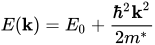
where E(k) is the energy of an electron at wavevector k in that band, E0 is a constant giving the edge of energy of that band, and m* is a constant (the effective mass).

It can be shown that the electrons placed in these bands behave as free electrons except with a different mass, as long as their energy stays within the range of validity of the approximation above. As a result, the electron mass in models such as the Drude model must be replaced with the effective mass.

One remarkable property is that the effective mass can become negative, when the band curves downwards away from a maximum. As a result of the negative mass, the electrons respond to electric and magnetic forces by gaining velocity in the opposite direction compared to normal; even though these electrons have negative charge, they move in trajectories as if they had positive charge (and positive mass). This explains the existence of valence-band holes, the positive-charge, positive-mass quasiparticles that can be found in semiconductors.[1]

In any case, if the band structure has the simple parabolic form described above, then the value of effective mass is unambiguous. Unfortunately, this parabolic form is not valid for describing most materials. In such complex materials there is no single definition of "effective mass" but instead multiple definitions, each suited to a particular purpose. The rest of the article describes these effective masses in detail.

Intermediate case: parabolic, anisotropic dispersion relation

[edit]
Constant energy ellipsoids in silicon near the six conduction band minima. For each valley (band minimum), the effective masses are m = 0.92me ("longitudinal"; along one axis) and mt = 0.19me ("transverse"; along two axes).[2]

In some important semiconductors (notably, silicon) the lowest energies of the conduction band are not symmetrical, as the constant-energy surfaces are now ellipsoids, rather than the spheres in the isotropic case. Each conduction band minimum can be approximated only by

where x, y, and z axes are aligned to the principal axes of the ellipsoids, and m*
x
, m*
y
and m*
z
are the inertial effective masses along these different axes. The offsets k0,x, k0,y, and k0,z reflect that the conduction band minimum is no longer centered at zero wavevector. (These effective masses correspond to the principal components of the inertial effective mass tensor, described later.[3])

In this case, the electron motion is no longer directly comparable to a free electron; the speed of an electron will depend on its direction, and it will accelerate to a different degree depending on the direction of the force. Still, in crystals such as silicon the overall properties such as conductivity appear to be isotropic. This is because there are multiple valleys (conduction-band minima), each with effective masses rearranged along different axes. The valleys collectively act together to give an isotropic conductivity. It is possible to average the different axes' effective masses together in some way, to regain the free electron picture. However, the averaging method turns out to depend on the purpose:[4]

  • For calculation of the total density of states and the total carrier density, via the geometric mean combined with a degeneracy factor g which counts the number of valleys (in silicon g = 6):[3]

    (This effective mass corresponds to the density of states effective mass, described later.)

    For the per-valley density of states and per-valley carrier density, the degeneracy factor is left out.
  • For the purposes of calculating conductivity as in the Drude model, via the harmonic mean
    Since the Drude law also depends on scattering time, which varies greatly, this effective mass is rarely used; conductivity is instead usually expressed in terms of carrier density and an empirically measured parameter, carrier mobility.

General case

[edit]

In general the dispersion relation cannot be approximated as parabolic, and in such cases the effective mass should be precisely defined if it is to be used at all. Here a commonly stated definition of effective mass is the inertial effective mass tensor defined below; however, in general it is a matrix-valued function of the wavevector, and even more complex than the band structure. Other effective masses are more relevant to directly measurable phenomena.

Inertial effective mass tensor

[edit]

A classical particle under the influence of a force accelerates according to Newton's second law, a = m−1F, or alternatively, the momentum changes according to d/dtp = F. This intuitive principle appears identically in semiclassical approximations derived from band structure when interband transitions can be ignored for sufficiently weak external fields.[5][6] The force gives a rate of change in crystal momentum pcrystal:
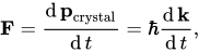
where ħ = h/2π is the reduced Planck constant.

Acceleration for a wave-like particle becomes the rate of change in group velocity:

where k is the del operator in reciprocal space. The last step follows from using the chain rule for a total derivative for a quantity with indirect dependencies, because the direct result of the force is the change in k(t) given above, which indirectly results in a change in E(k)=ħω(k). Combining these two equations yields

using the dot product rule with a uniform force (kF=0). is the Hessian matrix of E(k) in reciprocal space. We see that the equivalent of the Newtonian reciprocal inertial mass for a free particle defined by a = m−1F has become a tensor quantity
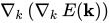
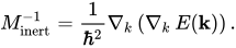
whose elements are

This tensor allows the acceleration and force to be in different directions, and for the magnitude of the acceleration to depend on the direction of the force.

  • For parabolic bands, the off-diagonal elements of Minert−1 are zero, and the diagonal elements are constants
  • For isotropic bands the diagonal elements must all be equal and the off-diagonal elements must all be equal.
  • For parabolic isotropic bands, Minert−1 = 1/m*I, where m* is a scalar effective mass and I is the identity.
  • In general, the elements of Minert−1 are functions of k.
  • The inverse, Minert = (Minert−1)−1, is known as the effective mass tensor. Note that it is not always possible to invert Minert−1


For bands with linear dispersion such as with photons or electrons in graphene, the group velocity is fixed, i.e. electrons travelling with parallel with k to the force direction F cannot be accelerated and the diagonal elements of Minert−1 are obviously zero. However, electrons travelling with a component perpendicular to the force can be accelerated in the direction of the force, and the off-diagonal elements of Minert−1 are non-zero. In fact the off-diagonal elements scale inversely with k, i.e. they diverge (become infinite) for small k. This is why the electrons in graphene are sometimes said to have infinite mass (due to the zeros on the diagonal of Minert−1) and sometimes said to be massless (due to the divergence on the off-diagonals).[7]

Cyclotron effective mass

[edit]

Classically, a charged particle in a magnetic field moves in a helix along the magnetic field axis. The period T of its motion depends on its mass m and charge e,

where B is the magnetic flux density.

For particles in asymmetrical band structures, the particle no longer moves exactly in a helix, however its motion transverse to the magnetic field still moves in a closed loop (not necessarily a circle). Moreover, the time to complete one of these loops still varies inversely with magnetic field, and so it is possible to define a cyclotron effective mass from the measured period, using the above equation.

The semiclassical motion of the particle can be described by a closed loop in k-space. Throughout this loop, the particle maintains a constant energy, as well as a constant momentum along the magnetic field axis. By defining A to be the k-space area enclosed by this loop (this area depends on the energy E, the direction of the magnetic field, and the on-axis wavevector kB), then it can be shown that the cyclotron effective mass depends on the band structure via the derivative of this area in energy:

Typically, experiments that measure cyclotron motion (cyclotron resonance, De Haas–Van Alphen effect, etc.) are restricted to only probe motion for energies near the Fermi level.

In two-dimensional electron gases, the cyclotron effective mass is defined only for one magnetic field direction (perpendicular) and the out-of-plane wavevector drops out. The cyclotron effective mass therefore is only a function of energy, and it turns out to be exactly related to the density of states at that energy via the relation , where gv is the valley degeneracy. Such a simple relationship does not apply in three-dimensional materials.

Density of states effective masses (lightly doped semiconductors)

[edit]
Density of states effective mass in various semiconductors[8][9][10][11]
Group Material Electron Hole
IV Si (4 K) 1.06 0.59
Si (300 K) 1.09 1.15
Ge 0.55 0.37
III–V GaAs 0.067 0.45
InSb 0.013 0.6
II–VI ZnO 0.29 1.21
ZnSe 0.17 1.44

In semiconductors with low levels of doping, the electron concentration in the conduction band is in general given by
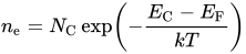
where EF is the Fermi level, EC is the minimum energy of the conduction band, and NC is a concentration coefficient that depends on temperature. The above relationship for ne can be shown to apply for any conduction band shape (including non-parabolic, asymmetric bands), provided the doping is weak (ECEFkT); this is a consequence of Fermi–Dirac statistics limiting towards Maxwell–Boltzmann statistics.

The concept of effective mass is useful to model the temperature dependence of NC, thereby allowing the above relationship to be used over a range of temperatures. In an idealized three-dimensional material with a parabolic band, the concentration coefficient is given by
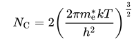
In semiconductors with non-simple band structures, this relationship is used to define an effective mass, known as the density of states effective mass of electrons. The name "density of states effective mass" is used since the above expression for NC is derived via the density of states for a parabolic band.

In practice, the effective mass extracted in this way is not quite constant in temperature (NC does not exactly vary as T3/2). In silicon, for example, this effective mass varies by a few percent between absolute zero and room temperature because the band structure itself slightly changes in shape. These band structure distortions are a result of changes in electron–phonon interaction energies, with the lattice's thermal expansion playing a minor role.[8]

Similarly, the number of holes in the valence band, and the density of states effective mass of holes are defined by:

where EV is the maximum energy of the valence band. Practically, this effective mass tends to vary greatly between absolute zero and room temperature in many materials (e.g., a factor of two in silicon), as there are multiple valence bands with distinct and significantly non-parabolic character, all peaking near the same energy.[8]

Determination

[edit]

Experimental

[edit]

Traditionally effective masses were measured using cyclotron resonance, a method in which microwave absorption of a semiconductor immersed in a magnetic field goes through a sharp peak when the microwave frequency equals the cyclotron frequency . In recent years effective masses have more commonly been determined through measurement of band structures using techniques such as angle-resolved photoemission spectroscopy (ARPES) or, most directly, the de Haas–van Alphen effect. Effective masses can also be estimated using the coefficient γ of the linear term in the low-temperature electronic specific heat at constant volume . The specific heat depends on the effective mass through the density of states at the Fermi level and as such is a measure of degeneracy as well as band curvature. Very large estimates of carrier mass from specific heat measurements have given rise to the concept of heavy fermion materials. Since carrier mobility depends on the ratio of carrier collision lifetime to effective mass, masses can in principle be determined from transport measurements, but this method is not practical since carrier collision probabilities are typically not known a priori. The optical Hall effect is an emerging technique for measuring the free charge carrier density, effective mass and mobility parameters in semiconductors. The optical Hall effect measures the analogue of the quasi-static electric-field-induced electrical Hall effect at optical frequencies in conductive and complex layered materials. The optical Hall effect also permits characterization of the anisotropy (tensor character) of the effective mass and mobility parameters.[12][13]

Theoretical

[edit]

A variety of theoretical methods including density functional theory, k·p perturbation theory, and others are used to supplement and support the various experimental measurements described in the previous section, including interpreting, fitting, and extrapolating these measurements. Some of these theoretical methods can also be used for ab initio predictions of effective mass in the absence of any experimental data, for example to study materials that have not yet been created in the laboratory.

Significance

[edit]

The effective mass is used in transport calculations, such as transport of electrons under the influence of fields or carrier gradients, but it also is used to calculate the carrier density and density of states in semiconductors. These masses are related but, as explained in the previous sections, are not the same because the weightings of various directions and wavevectors are different. These differences are important, for example in thermoelectric materials, where high conductivity, generally associated with light mass, is desired at the same time as high Seebeck coefficient, generally associated with heavy mass. Methods for assessing the electronic structures of different materials in this context have been developed.[14]

Certain group IIIV compounds such as gallium arsenide (GaAs) and indium antimonide (InSb) have far smaller effective masses than tetrahedral group IV materials like silicon and germanium. In the simplest Drude picture of electronic transport, the maximum obtainable charge carrier velocity is inversely proportional to the effective mass: , where with being the electronic charge. The ultimate speed of integrated circuits depends on the carrier velocity, so the low effective mass is the fundamental reason that GaAs and its derivatives are used instead of Si in high-bandwidth applications like cellular telephony.[15]


In April 2017, researchers at Washington State University claimed to have created a fluid with negative effective mass inside a Bose–Einstein condensate, by engineering the dispersion relation.[16]

See also

[edit]

Footnotes

[edit]

References

[edit]
[edit]
Revisions and contributorsEdit on WikipediaRead on Wikipedia
from Grokipedia
In solid-state physics, the effective mass (mm^*) is a fundamental quasiparticle parameter that characterizes the dynamical behavior of charge carriers, such as electrons and holes, in crystalline materials by quantifying their response to applied forces as if they were free particles with a modified mass distinct from the bare electron mass (m0m_0).[1][2] This concept emerges from the band structure of solids, where the periodic lattice potential alters the energy-momentum dispersion relation E(k)E(\mathbf{k}), allowing carriers near band extrema to be approximated by parabolic bands akin to free-particle motion but with an effective mass determined by the curvature of the energy surface: $ m^* = \hbar^2 \left( \frac{d^2 E}{dk^2} \right)^{-1} $.[3][2] The effective mass approximation simplifies the analysis of carrier transport and quantum mechanics in solids by replacing the complex Schrödinger equation in a periodic potential with an effective Hamiltonian that incorporates mm^*, enabling the use of semiclassical equations of motion such as F=mdvdt\mathbf{F} = m^* \frac{d\mathbf{v}}{dt}.[1] Derived from perturbation theory or the k·p method applied to Bloch waves near high-symmetry points in the Brillouin zone, mm^* can be positive, negative, greater than or less than m0m_0, and often anisotropic, manifesting as a tensor with components like longitudinal (mlm_l^*) and transverse (mtm_t^*) masses in materials with non-spherical constant-energy surfaces.[2][3] For instance, in silicon, the conduction band electrons have ml0.98m0m_l^* \approx 0.98 m_0 and mt0.19m0m_t^* \approx 0.19 m_0, while in gallium arsenide, m0.067m0m^* \approx 0.067 m_0 near the Γ-point, reflecting flatter bands and lighter carriers that enhance mobility.[3] This parameter is crucial for understanding and engineering semiconductor devices, as it directly influences key properties including electrical conductivity (σ=ne2τm\sigma = \frac{ne^2 \tau}{m^*}), carrier mobility (μ1m\mu \propto \frac{1}{m^*}), and the density of states (g(E)(m)3/2Eg(E) \propto (m^*)^{3/2} \sqrt{E}), which govern phenomena like doping effects, optical absorption, and quantum confinement in nanostructures.[1][2] In metals and insulators, mm^* explains deviations from free-electron behavior, while in semiconductors, it underpins the design of transistors, lasers, and solar cells by predicting how band engineering—via strain, alloying, or heterostructures—can tune carrier dynamics.[3] The approximation holds best for shallow impurities and low-energy excitations but breaks down for deep levels or strong fields, necessitating more advanced models like multiband or non-parabolic treatments.[2]

Fundamentals

Definition and motivation

In solid-state physics, the effective mass $ m^* $ characterizes the inertial response of an electron to external forces within a crystalline lattice, differing from the free-electron mass $ m_e $ due to the influence of the periodic potential created by the ion cores.[4] This concept arises because electrons in solids do not propagate as free particles but as extended Bloch waves, whose energy dispersion relation $ E(\mathbf{k}) $ near band extrema deviates from the parabolic form $ E = \frac{\hbar^2 k^2}{2m_e} $, leading to a renormalized mass that simplifies the description of their dynamics.[4] The motivation for introducing the effective mass lies in the need to model electron transport in crystals using semiclassical approximations, avoiding the full solution of the Schrödinger equation for complex band structures. By treating electrons as quasi-particles with mass $ m^* $, phenomena such as electrical conductivity and response to electric or magnetic fields can be analyzed analogously to free particles, capturing the curvature of the energy bands without detailed quantum calculations.[5] This approximation is particularly useful for understanding charge carrier mobility in materials where the lattice potential significantly alters electron behavior. The concept was pioneered by Felix Bloch in his 1928 doctoral thesis, which established the band theory of solids and laid the foundation for describing electron motion in periodic potentials through Bloch's theorem.[6] It became central to semiclassical transport theory, enabling predictions of material properties like semiconductors and metals. A key manifestation appears in the semiclassical equation of motion for Bloch electrons in the effective mass approximation:
mv˙=e(E+v×B), m^* \dot{\mathbf{v}} = -e \left( \mathbf{E} + \mathbf{v} \times \mathbf{B} \right),
where $ \mathbf{v} $ is the group velocity, $ \mathbf{B} $ is the magnetic field, $ e $ is the electron charge (positive), $ \mathbf{E} $ is the electric field, and $ m^* $ governs the response to the Lorentz force, encapsulating the band's curvature effects.[7] For example, in simple metals like copper, $ m^* \approx m_e $, reflecting nearly free-electron-like behavior, whereas in semiconductors such as gallium arsenide (GaAs), the conduction-band electron effective mass is much smaller at $ m^* = 0.067 m_e $, enhancing carrier mobility.[8]

Band structure prerequisites

In solid-state physics, the behavior of electrons in crystalline materials is fundamentally described by the Bloch theorem, which states that the wavefunctions of electrons in a periodic potential can be expressed as plane waves modulated by a periodic function. Specifically, the electron wavefunction takes the form ψ(r)=uk(r)eikr\psi(\mathbf{r}) = u_{\mathbf{k}}(\mathbf{r}) e^{i \mathbf{k} \cdot \mathbf{r}}, where uk(r)u_{\mathbf{k}}(\mathbf{r}) has the same periodicity as the crystal lattice, and k\mathbf{k} is the wavevector.[9] This representation arises from the translational symmetry of the lattice, allowing the Schrödinger equation to be solved by separating the rapidly varying plane-wave part from the lattice-periodic part.[9] The energy eigenvalues derived from these wavefunctions yield the dispersion relation E([k](/page/K))E(\mathbf{[k](/page/K)}), which maps the energy of electron states as a function of the wavevector [k](/page/K)\mathbf{[k](/page/K)} within the first Brillouin zone—a primitive cell in reciprocal space defined by the reciprocal lattice vectors. The Brillouin zone encapsulates the unique [k](/page/K)\mathbf{[k](/page/K)}-space for the crystal's periodic boundary conditions, and E([k](/page/K))E(\mathbf{[k](/page/K)}) forms continuous energy bands separated by band gaps. Near the extrema (minima or maxima) of these bands, the dispersion is approximately parabolic, resembling the free-electron parabola but modified by the lattice. The periodic lattice potential plays a crucial role by scattering electrons, which folds the extended free-electron energy parabola into the reduced zone scheme of the Brillouin zone, creating band gaps at zone boundaries due to Bragg-like reflections. This scattering alters the curvature of E(k)E(\mathbf{k}) at band edges, where the effective mass emerges as a measure of that curvature, influencing electron transport without explicit parabolic formulas here. Key concepts in band theory include the conduction band, the lowest-energy band above the band gap where electrons can move freely as charge carriers, and the valence band, the highest filled band below the gap containing bound electrons.[10] Band gaps are classified as direct if the conduction band minimum and valence band maximum occur at the same k\mathbf{k} (enabling efficient optical transitions) or indirect if they occur at different k\mathbf{k} points (requiring phonon assistance for momentum conservation).[10] The $ \mathbf{k} \cdot \mathbf{p} $ perturbation theory provides a foundational method to approximate band structures near high-symmetry points like k=0\mathbf{k}=0, treating the linear-in-k\mathbf{k} term as a perturbation on degenerate states to capture interband couplings that determine band curvatures.[11] In metals, the Fermi surface—defined by states at the Fermi energy within the Brillouin zone—exhibits complex geometry that influences effective mass via its curvature, but in semiconductors, the focus shifts to band edges where low carrier densities make the parabolic approximation near extrema particularly relevant for understanding transport and optical properties.

Parabolic Dispersion Cases

Isotropic case

In the isotropic case, the energy dispersion relation near a band extremum, such as the conduction band minimum at k=0\mathbf{k} = 0, is approximated by a parabolic form:
E(k)=E0+2k22m, E(\mathbf{k}) = E_0 + \frac{\hbar^2 k^2}{2 m^*},
where E0E_0 is the energy at the extremum, k=kk = |\mathbf{k}| is the magnitude of the wavevector, \hbar is the reduced Planck's constant, and mm^* is the scalar effective mass.[2] This approximation assumes spherical symmetry in k-space, simplifying the band structure to a form analogous to a free particle but with a modified mass that accounts for the lattice's influence on carrier motion.[2] The effective mass mm^* is derived from the curvature of the energy band at the extremum, specifically through the second derivative of the energy with respect to the wavevector:
m=2(d2Edk2)1, m^* = \hbar^2 \left( \frac{d^2 E}{dk^2} \right)^{-1},
evaluated at the band edge.[2] For a conduction band minimum, the upward curvature (concave up) yields a positive mm^*, reflecting the inertial response of electrons to external forces. In contrast, for a valence band maximum, the downward curvature (concave down) results in a negative mm^* for electrons, but this is conventionally interpreted as a positive effective mass m|m^*| for holes, which behave as positively charged carriers with opposite velocity relative to their wavevector.[1][2] In the free electron limit, where lattice effects are negligible, the dispersion reduces to the classical parabolic form with m=mem^* = m_e, the bare electron mass of approximately 9.11×10319.11 \times 10^{-31} kg. In semiconductors like silicon, the isotropic approximation for the conduction band electron effective mass is m0.26mem^* \approx 0.26 m_e, derived as an average over anisotropic valleys but useful for simplified models assuming spherical constancy.[12] The group velocity of carriers in this isotropic parabolic band is given by the gradient of the energy:
vg=1kE=km, \mathbf{v}_g = \frac{1}{\hbar} \nabla_{\mathbf{k}} E = \frac{\hbar \mathbf{k}}{m^*},
which parallels the free particle relation v=p/m\mathbf{v} = \mathbf{p}/m but with mm^* replacing mem_e. Under an applied electric field E\mathbf{E}, the semiclassical equation of motion for the crystal momentum is k˙=eE\hbar \dot{\mathbf{k}} = -e \mathbf{E} (for electrons), leading to an acceleration a=(eE)/m\mathbf{a} = - (e \mathbf{E})/m^* and enabling the effective mass to quantify the carrier's dynamical response in devices.[2][2]

Anisotropic case

In the anisotropic case, the effective mass approximation extends the isotropic parabolic dispersion to account for direction-dependent curvature in the band structure near extremal points, particularly along the principal crystal axes. This occurs when the second derivatives of the energy E(k)E(\mathbf{k}) with respect to wavevector components differ along orthogonal directions, leading to a diagonal effective mass tensor in the principal coordinate system.[13] The dispersion relation takes the form
E(k)=E0+22(kx2mx+ky2my+kz2mz), E(\mathbf{k}) = E_0 + \frac{\hbar^2}{2} \left( \frac{k_x^2}{m_x^*} + \frac{k_y^2}{m_y^*} + \frac{k_z^2}{m_z^*} \right),
where mxm_x^*, mym_y^*, and mzm_z^* are the principal effective masses along the respective axes, derived from the diagonal elements of the inverse effective mass tensor (m)ii1=122Eki2(\mathbf{m}^*)^{-1}_{ii} = \frac{1}{\hbar^2} \frac{\partial^2 E}{\partial k_i^2} evaluated at the band extremum in these coordinates.[14][13] This anisotropy results in ellipsoidal constant-energy surfaces in k\mathbf{k}-space, elongated along directions of heavier effective mass, which influences carrier transport properties. For instance, electron mobility is higher in directions aligned with lighter effective masses due to reduced inertial response to scattering.[14][15] A representative example is the conduction band of silicon, where each of the six equivalent valleys exhibits ellipsoidal geometry with a longitudinal effective mass ml0.98mem_l^* \approx 0.98 m_e along the 100\langle 100 \rangle direction and transverse effective masses mt0.19mem_t^* \approx 0.19 m_e in the perpendicular plane, reflecting the material's cubic symmetry.[16] To approximate isotropic behavior for certain calculations, such as density of states, an effective mass can be defined as the geometric mean (mxmymz)1/3(m_x^* m_y^* m_z^*)^{1/3}, though this serves only as an introductory setup for more general tensor treatments.[17]

General Effective Mass Tensor

Inertial effective mass

The inertial effective mass tensor describes the response of charge carriers to external forces in a crystal lattice, effectively capturing the curvature of the energy dispersion relation E(k)E(\mathbf{k}) near band extrema. Its inverse is defined as
(m)ij1=122Ekikj, \left( m^* \right)_{ij}^{-1} = \frac{1}{\hbar^2} \frac{\partial^2 E}{\partial k_i \partial k_j},
evaluated at the wavevector k0\mathbf{k}_0 corresponding to the band minimum or maximum, with the full tensor mm^* obtained by matrix inversion. This formulation arises from semiclassical dynamics, where the acceleration of an electron wavepacket under an applied force mimics that of a free particle but with a modified mass dictated by the band structure. In the equation of motion for Bloch electrons, the inertial effective mass tensor governs the time evolution of the crystal momentum and velocity, yielding
mv˙=e(E+v×B), m^* \dot{\mathbf{v}} = -e (\mathbf{E} + \mathbf{v} \times \mathbf{B}),
where v=1kE(k)\mathbf{v} = \frac{1}{\hbar} \nabla_{\mathbf{k}} E(\mathbf{k}) is the group velocity, E\mathbf{E} is the electric field, and B\mathbf{B} is the magnetic field. The tensor mm^* is symmetric due to the equality of mixed partial derivatives, rendering it Hermitian for real-valued energy bands, and it is positive definite near conduction band minima (where the dispersion curves upward) to reflect enhanced or reduced inertia compared to the free electron mass. In a coordinate system aligned with the principal axes of the tensor—determined by diagonalizing mm^*—the off-diagonal elements vanish, simplifying calculations to scalar effective masses along those directions. This tensor generalizes the anisotropic parabolic dispersion case, where E(k)E0+ij22mij(kik0i)(kjk0j)E(\mathbf{k}) \approx E_0 + \sum_{ij} \frac{\hbar^2}{2 m^*_{ij}} (k_i - k_{0i})(k_j - k_{0j}) yields a constant diagonal form in principal coordinates. However, the quadratic approximation holds only for small deviations from the extremum; farther from k0\mathbf{k}_0, non-parabolic effects cause the effective mass to become energy-dependent, invalidating the constant tensor for strongly curved, flat, or linear bands—such as Dirac cones in topological materials, where the second derivative vanishes at the conical apex, leading to massless-like behavior. In crystals with cubic symmetry, like silicon or gallium arsenide, point group symmetries impose constraints that eliminate off-diagonal tensor elements in high-symmetry coordinate systems (e.g., along 100\langle 100 \rangle directions), often resulting in a nearly isotropic tensor at the Γ\Gamma point for direct-bandgap materials. This symmetry-driven diagonality facilitates experimental interpretation and device modeling, though valley degeneracy in indirect-bandgap cubic semiconductors like silicon introduces overall anisotropy when averaging over multiple equivalent minima.

Cyclotron effective mass

The cyclotron effective mass $ m_c $ characterizes the orbital motion of charge carriers in a magnetic field and is defined as
mc=22πdAdE, m_c = \frac{\hbar^2}{2\pi} \frac{dA}{dE},
where $ A(E) $ is the cross-sectional area in k-space of the Fermi surface or constant-energy contour perpendicular to the magnetic field direction $ \mathbf{B} $. This definition emerges from the semiclassical quantization of electron orbits, where the phase space area enclosed by the orbit in a magnetic field leads to discrete Landau levels via the Bohr-Sommerfeld condition adapted to solids. The resulting cyclotron frequency is $ \omega_c = eB / m_c $, which determines the energy spacing $ \hbar \omega_c $ between Landau levels for parabolic bands. In anisotropic parabolic bands, the cyclotron effective mass relates to the principal components of the effective mass tensor as $ m_c = \sqrt{m_x^* m_y^*} $ when $ \mathbf{B} $ is applied along the z-direction, reflecting the geometry of the elliptical orbits in k-space. This contrasts with the inertial effective mass, which governs acceleration under electric fields and derives directly from the band curvature tensor. In non-parabolic bands, where the energy dispersion deviates from quadratic form, $ m_c $ at the Fermi energy differs from the inertial mass near the band edge due to energy-dependent curvature. The cyclotron effective mass is commonly measured through cyclotron resonance, where microwaves excite transitions between Landau levels at frequency $ \omega_c $. For example, in gallium arsenide (GaAs), cyclotron resonance yields an electron $ m_c \approx 0.067 m_e $, where $ m_e $ is the free-electron mass; in this nearly isotropic case, it coincides with the density-of-states effective mass.[18]

Density of states effective mass

The density of states effective mass, denoted $ m_{\rm dos}^* $, is employed in the calculation of the electronic density of states $ g(E) $ near band extrema in semiconductors, especially under lightly doped conditions where the Fermi level lies close to the band edge and contributions from a single parabolic energy pocket predominate.[19] This parameter effectively captures the influence of band curvature on the number of available states, enabling simplified statistical mechanics treatments for carrier concentrations. In multi-valley materials, such as silicon with its six equivalent conduction band minima along the 100\langle 100 \rangle directions, averaging over the valley degeneracy $ N_v = 6 $ is incorporated to yield the overall $ m_{\rm dos}^* $. For the isotropic case, where the energy dispersion is parabolic and symmetric, $ m_{\rm dos}^* = m^* $, the single effective mass parameter describing the band curvature.[20] In anisotropic parabolic bands, the dispersion relation takes an ellipsoidal form, and $ m_{\rm dos}^* = (m_x^* m_y^* m_z^)^{1/3} $, with $ m_x^ $, $ m_y^* $, and $ m_z^* $ as the principal components of the effective mass tensor along the crystal axes.[21] This geometric mean ensures the density of states reflects the volume scaling of the constant-energy surface in k-space. The resulting conduction band density of states above the edge energy $ E_c $ is then
g(E)=(2mdos)3/22π23EEc,EEc, g(E) = \frac{(2 m_{\rm dos}^*)^{3/2}}{2 \pi^2 \hbar^3} \sqrt{E - E_c}, \quad E \geq E_c,
which includes a factor of 2 for spin degeneracy and assumes free-electron-like phase space integration adjusted for the effective mass.[20] In the valence band, distinct light-hole ($ m_{\rm lh}^* )andheavyhole() and heavy-hole ( m_{\rm hh}^* $) bands arise due to spin-orbit coupling and crystal symmetry, contributing separately to the total density of states. The effective $ m_{\rm dos}^* $ for holes is $ ( (m_{\rm lh}^)^{3/2} + (m_{\rm hh}^)^{3/2} )^{2/3} $, weighting each band's contribution by the $ (m^)^{3/2} $ factor inherent to three-dimensional parabolic statistics.[22] For transport phenomena, a related conductivity effective mass $ m_{\rm cond}^ = \frac{\sum_i (m_i^)^{3/2}}{\sum_i (m_i^)^{1/2}} $ is used, where the sum runs over multiple bands or valleys; this arises from the parallel addition of conductivities, assuming equal relaxation times, and differs from $ m_{\rm dos}^* $ by emphasizing mobility contributions.[17] These formulations rely on the parabolic band approximation, valid near extrema but limited for higher energies or narrower-gap materials where non-parabolicity distorts the dispersion; in such cases, direct numerical integration over the full band structure is required to compute $ g(E) $.[19] In isotropic parabolic systems, $ m_{\rm dos}^* $ equals the cyclotron effective mass derived from orbital motion in magnetic fields.[23]

Determination Methods

Experimental approaches

Cyclotron resonance is a primary experimental technique for determining the cyclotron effective mass $ m_c^* $ in semiconductors and metals. In this method, charge carriers in a magnetic field absorb microwave radiation at the cyclotron frequency $ \omega_c = eB / m_c^* $, where $ e $ is the electron charge and $ B $ is the magnetic field strength. By measuring the resonance frequency as a function of $ B $, $ m_c^* $ is directly obtained from the slope of the linear relation $ \omega_c $ versus $ B .Seminalexperimentsinthe1950songermaniumandsiliconbyLaxandcollaboratorsat[microwave](/page/Microwave)frequencies(e.g.,24GHz)revealedanisotropiceffectivemassesfor[electron](/page/Electron)sandholes,withvaluesaround0.12. Seminal experiments in the 1950s on germanium and silicon by Lax and collaborators at [microwave](/page/Microwave) frequencies (e.g., 24 GHz) revealed anisotropic effective masses for [electron](/page/Electron)s and holes, with values around 0.12 m_e $ to 0.82$ m_e $ depending on orientation, establishing the technique's precision for band structure characterization.[24] Shubnikov-de Haas (SdH) oscillations in magnetoresistance provide another key approach to extract the effective mass through quantum transport measurements. These oscillations arise from Landau level quantization in high magnetic fields at low temperatures, manifesting as periodic variations in resistivity with inverse magnetic field $ 1/B $. The oscillation frequency relates to the Fermi surface cross-section, and the effective mass $ m^* $ is determined from the temperature-dependent amplitude damping of the oscillations, following the Lifshitz-Kosevich formula. For instance, in n-type GaAs, SdH analysis yields electron effective masses near 0.067$ m_e $, consistent with band theory. The period $ \Delta(1/B) = e \hbar / (m^* E_F) $ further links the data to the Fermi energy $ E_F $, enabling comprehensive Fermi surface mapping.[25] Optical methods, such as modulation spectroscopy, infer effective mass from perturbations to interband transitions that reveal band curvature. In electroreflectance or photoreflectance, electric fields modulate the dielectric function, sharpening excitonic features whose energies depend on reduced effective masses via the exciton binding energy $ E_b = \mu e^4 / (2 \hbar^2 \epsilon^2) $, where $ \mu $ is the reduced mass. Excitonic shifts in magnetic fields (magneto-optics) also probe dispersion, as the diamagnetic shift scales with $ (m_e^*)^{-1} .Forexample,inCdTequantumwells,thesetechniquesmeasureheavyholeeffectivemassesaround0.27. For example, in CdTe quantum wells, these techniques measure heavy-hole effective masses around 0.27 m_e $, providing insights into valence band structure without magnetic fields.[26] Angle-resolved photoemission spectroscopy (ARPES) directly visualizes the band dispersion $ E(\mathbf{k}) $ near the Fermi level, allowing computation of effective mass from the second derivative $ m^* = \hbar^2 / (\partial^2 E / \partial k^2) .HighresolutionARPESoncleavedsinglecrystalsmapsthefull[Brillouinzone](/page/Brillouinzone),yieldinganisotropicmasses;intopologicalinsulatorslikeBi2Se3,surfacestateeffectivemassesareextractedas 0.3. High-resolution ARPES on cleaved single crystals maps the full [Brillouin zone](/page/Brillouin_zone), yielding anisotropic masses; in topological insulators like Bi₂Se₃, surface state effective masses are extracted as ~0.3 m_e $ from parabolic fits to Dirac cones. This momentum-resolved technique excels for complex materials, though surface sensitivity limits bulk access.[27] As of 2025, advanced techniques extend effective mass measurements to non-equilibrium and local regimes. Time-resolved ARPES (TR-ARPES) captures ultrafast changes in dispersion following photoexcitation, revealing transient effective masses altered by carrier heating or many-body interactions; in graphene, pump-probe ARPES shows mass enhancements up to 20% on femtosecond timescales. Scanning tunneling microscopy (STM) provides spatially resolved effective masses in 2D materials via differential conductance $ dI/dV $ spectra, which reflect local density of states curvature; in silicene-like Ga layers on Si(111), STM yields conduction band masses of ~0.2$ m_e $, highlighting nanoscale variations due to substrate effects.[28][29]

Theoretical calculations

Theoretical calculations of the effective mass in solid-state physics rely on computational methods that predict band structures from first principles or semi-empirical approximations, enabling the extraction of the effective mass tensor through analysis of energy dispersion relations E(k).[13] The k·p method employs perturbation theory to approximate band dispersions near high-symmetry points, such as k=0 at the Γ point, by treating the crystal momentum operator as a perturbation on the unperturbed Bloch states. In the two-band model for non-degenerate conduction and valence bands, the inverse effective mass is given by
1m=1me(1+2mevcpv2EcEv), \frac{1}{m^*} = \frac{1}{m_e} \left(1 + \frac{2}{m_e} \sum_{v} \frac{| \langle c | \mathbf{p} | v \rangle |^2}{E_c - E_v} \right),
where $ m_e $ is the free electron mass, $ |p_{cv}|^2 $ is the squared momentum matrix element between conduction (|c⟩) and valence (|v⟩) states, and $ E_c - E_v $ is the band gap energy; this formulation arises from second-order perturbation theory and is particularly useful for semiconductors with small band gaps. The method requires inputs like band energies and matrix elements, often obtained from experiments or ab initio calculations, and has been extended to multi-band Hamiltonians for more complex systems. Ab initio approaches, such as density functional theory (DFT), compute the full band structure by solving the Kohn-Sham equations self-consistently, after which the effective mass tensor is derived numerically from the second derivatives of E(k) along principal directions, $ m_{ij}^{*-1} = \frac{1}{\hbar^2} \frac{\partial^2 E}{\partial k_i \partial k_j} $.[13] These calculations use plane-wave or pseudopotential bases to handle periodic solids and provide parameter-free predictions, though standard local-density approximations often underestimate band curvatures and thus overestimate effective masses in semiconductors.[30] Density functional perturbation theory enhances accuracy by directly computing response functions for the Hessian without finite differences, reducing numerical errors in anisotropic cases.[13] Tight-binding models approximate the band structure by expanding wavefunctions in atomic orbitals with parameterized hopping integrals between nearest neighbors, yielding an E(k) dispersion from which the effective mass is obtained via curvature analysis, similar to the ab initio case but with fewer computational demands. Parameters are fitted to reproduce experimental band structures or derived from Slater-Koster integrals, making the approach ideal for large systems like nanostructures where full DFT is prohibitive; for instance, in silicon, the model captures valence band warping and derives anisotropic masses near the Γ point.[31] The GW approximation improves upon DFT by accounting for many-body electron-electron interactions through the self-energy operator, yielding quasiparticle energies whose dispersions provide corrected effective masses, often increasing them by 10-20% in semiconductors like GaN due to better band gap descriptions.228:2%3C567::AID-PSSB567%3E3.0.CO;2-Z) This method involves computing the screened Coulomb interaction W and Green's function G perturbatively, with implementations like G₀W₀ starting from a DFT wavefunction; it is computationally intensive but essential for accurate curvatures in wide-band-gap materials.[32] Modern extensions leverage machine learning interatomic potentials or surrogate models trained on DFT datasets to enable high-throughput screening of effective masses in two-dimensional materials, such as transition metal dichalcogenides (TMDs) like MoS₂, where predictions of conductivity effective masses guide the discovery of candidates with low m* for high-mobility devices.[33] These models, often using graph neural networks or kernel ridge regression, extrapolate band curvatures from bulk prototypes to 2D limits, achieving errors below 10% relative to DFT while scaling to thousands of compositions.[34]

Applications and Significance

In semiconductors and devices

In semiconductor band engineering, the effective mass plays a crucial role in optimizing carrier mobility for high-performance devices, where lighter effective masses enable faster electron transport and reduced inertial response to electric fields. For instance, indium antimonide (InSb) exhibits an electron effective mass of approximately 0.014 times the free electron mass ($ m_e $), facilitating exceptionally high electron mobilities exceeding 70,000 cm²/V·s at room temperature, which is leveraged in ultrafast transistor designs for terahertz applications.[35] This light effective mass arises from the narrow bandgap and small curvature of the conduction band minimum in InSb, allowing band structure tailoring through alloying or heterostructures to enhance device speed without excessive power dissipation.[35] Doping significantly influences the effective mass in semiconductors, particularly through non-parabolic band effects in heavily doped regimes. In degenerate n-type semiconductors like gallium nitride (GaN), the Burstein-Moss shift elevates the Fermi level into the conduction band, leading to band filling and increased non-parabolicity that raises the electron effective mass from its intrinsic value, altering optical absorption and carrier dynamics. In multi-valley semiconductors such as silicon, valley degeneracy—typically six equivalent conduction band minima—further modifies the density of states effective mass as $ m_{dos}^* = (g_v)^{2/3} m_t^{2/3} m_l^{1/3} $, where $ g_v = 6 $, $ m_t^ $ is the transverse mass, and $ m_l^ $ is the longitudinal mass, enhancing carrier concentration capacity in doped channels for robust device operation.[36] Reduced dimensionality in quantum wells and two-dimensional (2D) systems profoundly alters the effective mass, often enhancing the density of states mass due to confinement-induced modifications in band dispersion. In GaAs quantum wells, for example, the in-plane effective mass remains similar to the bulk value at low densities, but interactions in denser 2D electron gases can increase it, impacting carrier localization and optical properties. Similarly, in quantum dots like InAs/GaAs structures, three-dimensional confinement leads to discrete energy levels that enhance exciton binding energies compared to bulk, enabling higher exciton binding and improved light emission efficiency in nanoscale optoelectronics. In metal-oxide-semiconductor field-effect transistors (MOSFETs), a low effective mass minimizes intervalley scattering and enhances channel mobility, directly improving switching speeds and reducing energy loss. Silicon-based MOSFETs benefit from strain-induced reductions in hole effective mass, which lessen phonon scattering rates and boost drive currents by up to 20-30% in p-channel devices.[37] For light-emitting diodes (LEDs), the hole effective mass critically influences radiative recombination rates, as heavier holes in GaN-based structures (around 1.0-2.0 $ m_e $) limit hole injection and distribution across the active region, contributing to efficiency droop under high currents; optimizing this through polarization engineering enhances carrier balance and output power.[38] Recent advancements highlight the effective mass's role in emerging semiconductors for photovoltaics and flexible electronics. In halide perovskites like methylammonium lead iodide (MAPbI₃), the light electron and hole effective masses (0.1-0.3 $ m_e $) promote long carrier diffusion lengths exceeding 1 μm, enabling high power conversion efficiencies over 20% in solar cells by facilitating efficient charge separation at interfaces.[39] Strain engineering in III-V semiconductors, such as InGaAs, allows tunable effective masses through lattice mismatch in epitaxial layers, reducing electron mass by up to 20% under tensile strain to improve mobility in high-electron-mobility transistors (HEMTs) for 5G and beyond applications.[40]

In transport properties

In solid-state physics, the effective mass $ m^* $ plays a crucial role in determining charge carrier mobility, defined as $ \mu = \frac{e \tau}{m^} $, where $ e $ is the elementary charge and $ \tau $ is the relaxation time.[41] A smaller $ m^ $ enhances mobility by allowing carriers to accelerate more readily under an electric field, which is vital for high-speed electronics. For instance, in gallium arsenide (GaAs), the electron effective mass is approximately $ 0.067 m_e $ (where $ m_e $ is the free electron mass), contributing to an electron mobility of about 9000 cm²/V·s at 300 K, enabling applications in fast-switching transistors.[42] Electrical conductivity $ \sigma $ in semiconductors follows the Drude model expression $ \sigma = \frac{n e^2 \tau}{m^} $, where $ n $ is the carrier density, highlighting the inverse dependence on $ m^ $.[41] In anisotropic materials, such as layered semiconductors, the conductivity becomes tensorial, relying on a conductivity effective mass $ m_{\text{cond}} $ derived from the inverse mass tensor components, which accounts for directional variations in carrier response.[43] This anisotropy can lead to highly directional transport properties, as observed in two-dimensional quantum wires where effective mass differences along principal axes significantly alter current flow.[44] The Hall effect provides insights into effective mass through carrier dynamics, with the classical Hall coefficient $ R_H = \frac{1}{n e} $ independent of $ m^* $, but mobility (and thus scattering influenced by $ m^* $) modulates the measured Hall voltage.[45] In the quantum Hall regime, the cyclotron effective mass $ m_c = \frac{e B}{\omega_c} $ (where $ B $ is the magnetic field and $ \omega_c $ the cyclotron frequency) directly governs Landau level formation and quantized conductance plateaus.[46] Thermoelectric transport properties are also modulated by effective mass, particularly the density-of-states effective mass $ m_{\text{dos}} $, which enters the Seebeck coefficient $ S \propto \frac{m_{\text{dos}}}{n^{2/3}} $.[47] Optimizing $ m^* $ balances high $ S $ (from larger $ m_{\text{dos}} $) with sufficient mobility, enhancing the figure of merit $ ZT = \frac{S^2 \sigma T}{\kappa} $ (where $ T $ is temperature and $ \kappa $ thermal conductivity), as low $ m^* $ reduces lattice scattering while avoiding excessive carrier velocities that diminish $ S $.[48] However, the standard effective mass concept has limitations in certain systems. In disordered solids, scattering mechanisms can invalidate the parabolic band approximation underlying $ m^* $, leading to non-Drude transport. In topological materials like graphene, charge carriers behave as massless Dirac fermions with linear dispersion $ E = \hbar v_F |k| $ (where $ v_F $ is the Fermi velocity), resulting in an effective mass approaching zero and relativistic-like dynamics rather than classical massive particle behavior.

References

User Avatar
No comments yet.