

Community hub
Recent from talks
Contribute something
Nothing was collected or created yet.
NXP LPC
View on WikipediaThis article may rely excessively on sources too closely associated with the subject, potentially preventing the article from being verifiable and neutral. (December 2018) |
LPC (Low Pin Count) is a family of 32-bit microcontroller integrated circuits by NXP Semiconductors (formerly Philips Semiconductors).[1] The LPC chips are grouped into related series that are based around the same 32-bit ARM processor core, such as the Cortex-M4F, Cortex-M3, Cortex-M0+, or Cortex-M0. Internally, each microcontroller consists of the processor core, static RAM memory, flash memory, debugging interface, and various peripherals. The earliest LPC series were based on the Intel 8-bit 80C51 core.[2] As of February 2011, NXP had shipped over one billion ARM processor-based chips.[3]

Overview
[edit]All recent LPC families are based on ARM cores, which NXP Semiconductors licenses from ARM Holdings, then adds their own peripherals before converting the design into a silicon die. NXP is the only vendor shipping an ARM Cortex-M core in a dual in-line package: LPC810 in DIP8 (0.3-inch width) and LPC1114 in DIP28 (0.6-inch width). The following tables summarize the NXP LPC microcontroller families.
History
[edit]- In 1982, Philips Semiconductors invented the I²C-bus, and is currently the top supplier of I²C solutions in the world.[11]
- In January 2005, Philips Semiconductors launched the PNX4008 'Nexperia™ Mobile Multimedia Processor', featuring an ARM9 processor and including PowerVR MBX graphics IP from Imagination Technologies.
- In February 2005, Philips Semiconductors announces the LPC3000 ARM9 series, based on the Nexperia platform.[12]
- In September 2006, Philips Semiconductors was spun off to a consortium of private equity investors and changed its name to NXP.[1] As part of this spin off, NXP acquired the older Philips LPC microcontroller families.
- In September 2006, NXP announced the LPC2300 and LPC2400 ARM7 series.[13]
- In September 2007, NXP announced the LPC2900 series.[14]
- In February 2008, NXP announced the licensing of the ARM Cortex-M3 core from ARM Holdings.[15]
- In March 2008, NXP announced the LPC3200 ARM9 series.[16]
- In October 2008, NXP announced the LPC1700 series.[17]
- In February 2009, NXP announced the licensing of the ARM Cortex-M0 core from ARM Holdings.[18]
- In May 2009, NXP announced the LPC1300 series.[19]
- In January 2010, NXP launched the LPCXpresso Toolchain for NXP ARM processors.[20]
- In February 2010, NXP announced the licensing of the ARM Cortex-M4F core from ARM Holdings.[21]
- In April 2010, NXP announced the LPC1102, the world’s smallest ARM microcontroller at 2.17 mm x 2.32 mm size.[22]
- In September 2010, NXP announced the LPC1800 series.[23]
- In February 2011, NXP announced the LPC1200 series.[24]
- In April 2011, NXP announced the LPC11U00 series with USB.[25]
- In September 2011, NXP announced the LPC11D00 series with a LCD controller.[26]
- In December 2011, NXP announced the LPC4300 series, the first dual-core chip with an ARM Cortex-M4F and ARM Cortex-M0.[27]
- In February 2012, NXP announced the LPC1100LV series with dual supply voltage to allow interfacing to both 1.8 V and 3.3 V peripherals.[28]
- In March 2012, NXP announced the LPC1100XL series for extra low-power and LPC11E00 series with EEPROM.[29]
- In March 2012, NXP announced the licensing of the ARM Cortex-M0+ core from ARM Holdings.[30]
- In March 2012, NXP introduced a "longevity program" to promise availability of IC chips from select ARM families for 10 or more years.[31]
- In March 2012, NXP announced the LPC11A00 series with flexible analog subsystem.[32]
- In April 2012, NXP announced the LPC11C00 series with a CAN bus controller.[33]
- In September 2012, NXP announced the LPC4000 series based on ARM Cortex-M4F.[34]
- In November 2012, NXP announced the LPC800 series based on the ARM Cortex-M0+ core, and the first ARM Cortex-M in a DIP8 package.[35]
- In April 2013, NXP announced the LPC-Link 2 JTAG / SWD debug adapter. Multiple firmware versions are available to emulate popular debug adapters.[36][37]
- In May 2013, NXP announced that it acquired Code Red Technologies, an embedded software development tools provider, such as the LPCXpresso IDE and Red Suite.[38][39]
- In October 2013, NXP announced the LPC4370 microcontroller.[40]
- In December 2013, NXP announced the LPC11E37H and the LPC11U37H microcontrollers.[41]
- In January 2017, NXP announced LPC54000 MCU series along with a refresh of the LPC800 series.[42]
LPC4000 series
[edit]| General information | |
|---|---|
| Launched | Current |
| Performance | |
| Max. CPU clock rate | 120 to 204 MHz |
| Architecture and classification | |
| Microarchitecture | ARM Cortex-M4F[4] ARM Cortex-M0[6] |
| Instruction set | Thumb, Thumb-2, Sat Math, DSP, FPU |
.jpg)
The LPC4xxx series are based on the ARM Cortex-M4F core.
LPC4300
[edit]The LPC4300 series have two or three ARM cores, one ARM Cortex-M4F and one or two ARM Cortex-M0. The LPC4350 chips are pin-compatible with the LPC1850 chips. The LPC4330-Xplorer development board is available from NXP. The summary for this series is:[27][44][45]
- Core:
- ARM Cortex-M4F and one or two ARM Cortex-M0 core at a maximum clock rate of 204 MHz.
- Debug interface is JTAG or SWD with SWO "Serial Trace", eight breakpoints and four watch points. JTAG supports both cores, but SWD only supports Cortex-M4F core.
- Memory:
- Static RAM sizes of 104 / 136 / 168 / 200 / 264 KB.
- Flash sizes of 0 / 512 / 768 / 1024 KB.
- EEPROM size of 16 KB.
- ROM size of 64 KB, which contains a boot loader with optional booting from USART0 / USART3, USB0 / USB1, SPI Flash, Quad SPI Flash, external 8 / 16/ 32-bit NOR flash. The ROM also contains an API for in-system programming, in-application programming, OTP programming, USB device stack for HID / MSC / DFU.
- OTP size of 64 bits.
- Each chip has a factory-programmed 128-bit unique device identifier number.
- Peripherals:
- Oscillators consists of optional external 1 to 25 MHz crystal or oscillator, external 32.768 kHz crystal for RTC, internal 12 MHz oscillator, and three internal PLLs for CPU / USB / Audio.
- IC packages: LQFP100, TFBGA100, LQFP144, TFBGA180, LQFP208, LBGA256.
- Operating voltage range is 2.2 to 3.6 volt.
LPC4000
[edit]The LPC4000 series are based on the single ARM Cortex-M4F processor core. The LPC408x chips are pin-compatible with the LPC178x chips. The summary for this series is:[34][46]
- Core:
- ARM Cortex-M4F core at a maximum clock rate of 120 MHz.
- Debug interface is JTAG or SWD with SWO "Serial Trace", eight breakpoints and four watch points.
- Memory:
- Static RAM sizes of 24 / 40 / 80 / 96 KB.
- Flash sizes of 64 / 128 / 256 / 512 KB.
- EEPROM sizes of 2 / 4 KB.
- ROM boot loader.
- Each chip has a factory-programmed 128-bit unique device identifier number.
- Peripherals:
- Oscillators consists of optional external 1 to 25 MHz crystal or oscillator, external 32.768 kHz crystal for RTC, internal 12 MHz oscillator, and two internal PLLs for CPU and USB.
- IC packages: LQFP80, LQFP144, TFBGA180, LQFP208, TFBGA208.
- Operating voltage range is 2.4 to 3.6 volt.
LPC3000 series
[edit]| General information | |
|---|---|
| Launched | Current |
| Max. CPU clock rate | to 266 MHz |
| Architecture and classification | |
| Microarchitecture | ARM9 |
| Instruction set | Thumb, ARM |
The LPC3xxx series use the ARM926EJ-S core, and were based on the Nexperia SoC platform. Was the first 90 nm ARM9 MCU processor family.[48]
LPC3200
[edit]The LPC3200 series are based on the ARM926EJ-S processor core.[16][49]
LPC3100
[edit]The LPC3100 series are based on the ARM926EJ-S processor core.[50] The LPC3154 is used by NXP to implement the LPC-Link debugger on all LPCXpresso boards.[51][52] The LPC3180 core operates up to 208 MHz, and features interfaces for SDRAM, USB 2.0 full-speed, NAND flash, Secure Digital (SD) and I²C.[citation needed]
LPC2000 series
[edit]| General information | |
|---|---|
| Launched | Current |
| Max. CPU clock rate | to 72 MHz |
| Architecture and classification | |
| Microarchitecture | ARM7, ARM9 |
| Instruction set | Thumb, ARM |
LPC2000 is a series based on a 1.8-volt ARM7TDMI-S core operating at up to 80 MHz together with a variety of peripherals including serial interfaces, 10-bit ADC/DAC, timers, capture compare, PWM, USB interface, and external bus options. Flash memory ranges from 32 kB to 512 kB; RAM ranges from 4 kB to 96 kB.[citation needed]
NXP has two related series without the LPC name, the LH7 series are based on the ARM7TDMI-S and ARM720T cores,[54] and the LH7A series are based on the ARM9TDMI core.[55]
LPC2900
[edit]The LPC2900 series are based on the ARM968E-S processor core.[14][56]
LPC2400
[edit]The LPC2400 series are based on the ARM7TDMI-S processor core.[13][57]
LPC2300
[edit]The LPC2300 series are based on the ARM7TDMI-S processor core.[13][58] The LPC2364/66/68 and the LPC2378 are full-speed USB 2.0 devices with 2 CAN interfaces and 10/100 Ethernet MAC in LQFP100 and LQFP144 packages. Multiple peripherals are supported including a 10-bit 8-channel ADC and a 10-bit DAC.[citation needed]
LPC2200
[edit]The LPC2200 series are based on the ARM7TDMI-S processor core.[59]
LPC2100
[edit]The LPC2100 series are based on the ARM7TDMI-S processor core.[60] The LPC2141, LPC2142, LPC2144, LPC2146, and LPC2148 are full-speed USB 2.0 devices in LQFP64 packages. Multiple peripherals are supported including one or two 10-bit ADCs and an optional 10-bit DAC.[citation needed]
LPC1000 series
[edit]| General information | |
|---|---|
| Launched | Current |
| Performance | |
| Max. CPU clock rate | 30 to 180 MHz |
| Architecture and classification | |
| Microarchitecture | ARM Cortex-M3[5] ARM Cortex-M0[6] |
| Instruction set | Thumb, Thumb-2 |
_MCU.jpg)
The NXP LPC1000 family consists of six series of microcontrollers: LPC1800, LPC1700, LPC1500, LPC1300, LPC1200, LPC1100. The LPC1800, LPC1700, LPC1500, LPC1300 series are based on the Cortex-M3 ARM processor core.[61] The LPC1200 and LPC1100 are based on the Cortex-M0 ARM processor core.[62]
LPC1800
[edit]The NXP LPC1800-series are based on the ARM Cortex-M3 core.[23][63] The LPC1850 is pin-compatible with the LPC4350 parts. The available packages are TBGA100, LQFP144, BGA180, LQFP208, BGA256. The LPC4330-Xplorer development board is available from NXP.
The Apple M7 and M8 motion co-processor chips are most likely based on the LPC1800 series, as LPC18A1 and LPC18B1.
LPC1700
[edit]The NXP LPC1700-series are based on the ARM Cortex-M3 core.[17][64] The LPC178x is pin-compatible with the LPC408x parts. The available packages are LQFP80, LQFP100, TFBGA100, LQFP144, TFBGA180, LQFP208, TFBGA208. The LPC1769-LPCXpresso development board is available from NXP. The mbed LPC1768 board is also available. With EmCrafts LPC-LNX-EVB a LPC1788 based board with μClinux is available.[65]
LPC1500
[edit]The NXP LPC1500-series are based on the ARM Cortex-M3 core.[66] The available packages are LQFP48, LQFP64, LQFP100. The LPC1549-LPCXpresso development board is available from NXP along with a motor control kit.
LPC1300
[edit]The NXP LPC1300-series are based on the ARM Cortex-M3 core.[19][67] The available packages are HVQFN33, LQFP48, LQFP64. The LPC1343-LPCXpresso and LPC1347-LPCXpresso development board are available from NXP.
LPC1200
[edit]The NXP LPC1200-family are based on the ARM Cortex-M0 core. It consists of 2 series: LPC1200, LPC12D00.[24][68][69] The available packages are LQFP48, LQFP64, LQFP100. The LPC1227-LPCXpresso development board is available from NXP.
LPC1100
[edit]The NXP LPC1100-family are based on the ARM Cortex-M0 core. It consists of 8 series: LPC1100 Miniature, LPC1100(X)L, LPC1100LV, LPC11A00, LPC11C00, LPC11D00, LPC11E00, LPC11U00.
LPC1100 Miniature
[edit]The LPC1100 series primarily targets an ultra tiny footprint. The available package is WLCSP16 (2.17 mm x 2.32 mm).[22][70] The LPC1104-LPCXpresso development board is available from NXP.
LPC1100(X)L
[edit]The LPC1100(X)L-series consists of three subseries: LPC111x, LPC111xL, and LPC111xXL. The LPC111xL and LPC111xXL include the power profiles, a windowed watchdog timer, and a configurable open-drain mode. The LPC1110XL adds a Non-Maskable Interrupt (NMI) and 256-byte page flash erase function. The LPC1114-LPCXpresso and LPC1115-LPCXpresso development board are available from NXP. The summary for these series are:[29][71]
- Core:
- ARM Cortex-M0 core at a maximum clock rate of 50 MHz.
- Includes 24-bit SysTick Timer.
- Debug interface is SWD with four breakpoints and two watchpoints. JTAG debugging is not supported.
- Memory:
- Static RAM sizes of 1 / 2 / 4 / 8 KB general purpose.
- Flash sizes of 4 / 8 / 16 / 24 / 32 / 64 KB general purpose.
- ROM boot loader.
- Each chip has a factory-programmed 128-bit unique device identifier number.
- Peripherals:
- LPC111x has one UART, one I²C, one or two SPI, two 16-bit timers, two 32-bit timers, watch dog timer, five to eight multiplexed 10-bit ADC, 14 to 42 GPIO.
- I²C supports standard mode (100 kHz) / fast-mode (400 kHz) / fast-mode Plus (1 MHz) speeds, master / slave / snooping modes, multiple slave addresses.
- LPC111xL consists of LPC111x features, plus low power profile in active and sleep modes, internal pull-up resistors to pull-up pins to full VDD level, programmable pseudo open-drain mode for GPIO pins, upgraded to windowed watch dog timer with clock source lock capability.
- LPC111xXL consists of LPC1110L features, plus flash page erase In-Application Programming (IAP) function, timers / UART / SSP peripherals available on more pins, one capture feature added to each timer, capture-clear feature on 16-bit and 32-bit timers for pulse-width measurements.
- LPC111x has one UART, one I²C, one or two SPI, two 16-bit timers, two 32-bit timers, watch dog timer, five to eight multiplexed 10-bit ADC, 14 to 42 GPIO.
- Oscillators consists of optional external 1 to 25 MHz crystal or oscillator, internal 12 MHz oscillator, internal programmable 9.3 kHz to 2.3 MHz watchdog oscillator, and one internal PLL for CPU.
- IC packages:
- Operating voltage range is 1.8 to 3.6 volt.
LPC1100LV
[edit]The LPC1100LV series primarily targets a low operating voltage range of 1.65 to 1.95 volt power. Its I²C is limited to 400 kHz. It is available in two power supply options: A 1.8 volt single power supply (WLCSP25 and HVQFN24 packages), or 1.8 volt (core) / 3.3 volt (IO/analog) dual power supply with 5 volt tolerant I/O (HVQFN33 package). The available packages are WLCSP25 (2.17 mm × 2.32 mm), HVQFN24 and HVQFN33.[28][72]
LPC11A00
[edit]The LPC11A00 series primarily targets analog features, such as: 10-bit ADC, 10-bit DAC, analog comparators, analog voltage reference, temperature sensor, EEPROM memory. The available packages are WLCSP20 (2.5 mm x 2.5 mm), HVQFN33 (5 mm x 5 mm), HVQFN33 (7 mm x 7 mm), LQFP48.[32][73]
LPC11C00
[edit]The LPC11C00 series primarily targets CAN bus features, such as: one MCAN controller, and the LPC11C22 and LPC11C24 parts include an on-chip high-speed CAN transceiver. The available package is LQFP48.[33][74] The LPC11C24-LPCXpresso development board is available from NXP.
LPC11D00
[edit]The LPC11D00 series primarily targets LCD display features, such as: 4 x 40 segment LCD driver. The available package is LQFP100.[26][75]
LPC11E00
[edit]The LPC11E00 series primarily targets EEPROM memory and Smart Card features.[29][76]
LPC11U00
[edit]The LPC11U00 series primarily targets USB features, such as: USB 2.0 full-speed controller. It's the first Cortex-M0 with integrated drivers in ROM. This series is pin-compatible with the LPC134x series.[25][77] The LPC11U14-LPCXpresso development board is available from NXP. The mbed LPC11U24 board is also available.
LPC800 series
[edit]| General information | |
|---|---|
| Launched | 2012 |
| Discontinued | Current |
| Performance | |
| Max. CPU clock rate | 30 MHz |
| Architecture and classification | |
| Microarchitecture | ARM Cortex-M0+[7] |
| Instruction set | Thumb subset, Thumb-2 subset |
LPC800
[edit]The NXP LPC800 microcontroller family are based on the Cortex-M0+ ARM processor core. Unique features include a pin switch matrix, state configurable timer, clockless wake-up controller, single-cycle GPIO, DIP8 package. The LPC812-LPCXpresso development board is available from NXP. The summary for this series is:[35][79][80]
- Core:
- ARM Cortex-M0+ core at a maximum clock rate of 30 MHz.
- Includes a single-cycle 32x32 bit multiplier, 24-bit SysTick Timer, Vector Table Relocation, full NVIC with 32 interrupts and four levels of priorities, single-cycle GPIO.
- Doesn't include a memory protection unit (MPU), nor a wake-up interrupt controller (WIC). Instead NXP added their own clockless wake-up controller to lower power usage.
- The debug interface is SWD with four breakpoints, two watchpoints, 1 KB Micro Trace Buffer (MTB). JTAG debugging is not supported.
- Memory:
- Static RAM sizes of 1 / 2 / 4 KB general purpose.
- Flash sizes of 4 / 8 / 16 KB general purpose, zero wait-state up to 20 MHz, one wait-state up to 30 MHz.
- ROM size of 8 KB, which contains a boot loader with optional booting from USART. The ROM also contains an API for USART communication, I²C communication, flash programming, in-system programming, and power profile.
- Each chip has a factory-programmed 128-bit unique device identifier number.
- Peripherals:
- One to three USARTs, one I²C, one or two SPI, one analog comparator, four interrupt timers, state configurable timer, wake-up timer, windowed watchdog timer, 6 to 18 single-cycle GPIOs, cyclic redundancy check (CRC) engine, pin switch matrix, four low-power modes, brownout detect.
- I²C supports standard mode (100 kHz) / fast-mode (400 kHz) / fast-mode Plus (1 MHz) speeds, master / slave / snooping modes, multiple slave addresses.
- Oscillators consists of optional external 1 to 25 MHz crystal or oscillator, internal 12 MHz oscillator, internal programmable 9.3 kHz to 2.3 MHz watchdog oscillator, and one internal PLL for CPU.
- IC packages are DIP8 (0.3-inch width), TSSOP16, TSSOP20, SO20. NXP is the only vendor shipping ARM Cortex-M cores in DIP packages.
- Operating voltage range is 1.8 to 3.6 volt.
Legacy series
[edit]LPC900
[edit]The LPC900 series are legacy devices based on the 8-bit 80C51 processor core.[81]
LPC700
[edit]The LPC700 series are legacy devices based on the 8-bit 80C51 processor core.[82]
Development boards
[edit]LPCXpresso boards
[edit]_MCU.jpg)
LPCXpresso boards are sold by NXP to provide a quick and easy way for engineers to evaluate their microcontroller chips.[83][84] The LPCXpresso boards are jointly developed by NXP, Code Red Technologies,[38] and Embedded Artists.[20]
Each LPCXpresso board has the following common features:
- On-board LPC-LINK for programming and debugging via a MiniUSB connector.
- Board can be cut into two separate boards: LPC-LINK board and target microcontroller board.
- Power input from 5 V via the USB cable or 5 V external power. If boards are separated, then 3.3 V external power is required for the target microcontroller board.
- Target microcontroller side:
|
The following LPCXpresso boards exist:[51]
|
The following mbed boards exist:[97]
The following BaseBoards are compatible with LPCXpresso and mbed boards:
|
Development tools
[edit]Cortex-M
[edit]LPC
[edit]- Flash programming via UART
All LPC microcontrollers have a ROM'ed bootloader that supports loading a binary image into its flash memory using one or more peripherals (varies by family). Since all LPC bootloaders support loading from the UART peripheral and most boards connect a UART to RS-232 or a USB-to-UART adapter IC, thus it's a universal method to program the LPC microcontrollers. Some microcontrollers requires the target board to have a way to enable/disable booting from the ROM'ed bootloader (i.e. jumper / switch / button).
- lpc21isp A multi-platform open-source tool to flash LPC microcontrollers over the UART.
- Flash Magic, a commercial program for Windows and macOS to perform in-system programming of the LPC flash via its UART.
- nxp_isp_loader, an open-source tool to flash LPC microcontrollers over the UART.
- Debugging tools (JTAG / SWD)
- OpenOCD, an open source software package for JTAG access using a wide variety of hardware adapters.
- LPC-Link 2, by NXP, a JTAG / SWD debug adapter that has multiple firmware releases available to emulate popular debug adapter protocols, such as: J-Link by Segger, CMSIS-DAP by ARM, Redlink by Code Red Technologies. All connectors are 1.27 mm (0.05-inch) pitch.[36][37]
Documentation
[edit]The amount of documentation for all ARM chips is daunting, especially for newcomers. The documentation for microcontrollers from past decades would easily be inclusive in a single document, but as chips have evolved so has the documentation grown. The total documentation is especially hard to grasp for all ARM chips since it consists of documents from the IC manufacturer (NXP Semiconductors) and documents from CPU core vendor (ARM Holdings).
A typical top-down documentation tree is: manufacturer website, manufacturer marketing slides, manufacturer datasheet for the exact physical chip, manufacturer detailed reference manual that describes common peripherals and aspects of a physical chip family, ARM core generic user guide, ARM core technical reference manual, ARM architecture reference manual that describes the instruction set(s).
- NXP documentation tree (top to bottom)
- NXP website.
- NXP marketing slides.
- NXP datasheet.
- NXP reference manual.
- ARM core website.
- ARM core generic user guide.
- ARM core technical reference manual.
- ARM architecture reference manual.
NXP has additional documents, such as: evaluation board user manuals, application notes, getting started guides, software library documents, errata, and more. See External Links section for links to official NXP and ARM documents.
See also
[edit]References
[edit]- ^ a b Press Release; NXP; September 1, 2006.
- ^ LPC900 series; NXP Semiconductors
- ^ "NXP, ARM sign long term Cortex-M processor deal", New Electronics, February 28, 2011. Retrieved November 12, 2011.
- ^ a b Cortex-M4F Specification Summary; ARM Holdings.
- ^ a b Cortex-M3 Specification Summary; ARM Holdings.
- ^ a b c Cortex-M0 Specification Summary; ARM Holdings.
- ^ a b Cortex-M0+ Specification Summary; ARM Holdings.
- ^ ARM926EJ-S Specification Summary; ARM Holdings.
- ^ ARM968E-S Specification Summary; ARM Holdings.
- ^ ARM7TDMI-S Specification Summary; ARM Holdings.
- ^ "NXP unveils UCODE I2C RFID chip", PC's Semiconductors Blog, April 5, 2011. Retrieved February 2, 2013.
- ^ "Philips Takes Lead in ARM9 Family-Based Microcontrollers with First 90nm MCU Family | Business Wire". Business Wire. 26 February 2018. Archived from the original on 2018-02-26. Retrieved 1 May 2023.
- ^ a b c Press Release; NXP; September 25, 2006.
- ^ a b Press Release; NXP; September 17, 2007.
- ^ Press Release; NXP; February 5, 2008.
- ^ a b Press Release; NXP; March 26, 2008.
- ^ a b Press Release; NXP; October 6, 2008.
- ^ Press Release; NXP; February 23, 2009.
- ^ a b Press Release; NXP; May 26, 2009.
- ^ a b Press Release; NXP; January 25, 2010.
- ^ Press Release; NXP; February 22, 2010.
- ^ a b Press Release; NXP; April 20, 2010.
- ^ a b Press Release; NXP; September 20, 2010.
- ^ a b Press Release; NXP; February 22, 2011.
- ^ a b Press Release; NXP; April 11, 2011.
- ^ a b Press Release; NXP; September 26, 2011.
- ^ a b Press Release; NXP; December 5, 2011.
- ^ a b Press Release; NXP; February 14, 2012.
- ^ a b c Press Release; NXP; March 1, 2012.
- ^ Press Release; NXP; March 13, 2012.
- ^ Press Release; NXP; March 27, 2012.
- ^ a b Press Release; NXP; March 27, 2012.
- ^ a b Press Release; NXP; April 26, 2012.
- ^ a b Press Release; NXP; September 19, 2012.
- ^ a b Press Release; NXP; November 13, 2012.
- ^ a b Press Release; NXP; April 24, 2013.
- ^ a b LPC-Link 2; NXP.
- ^ a b Press Release; NXP; May 1, 2013.
- ^ Code Red Technologies.
- ^ Press Release; NXP; October 21, 2013.
- ^ Press Release; NXP; December 5, 2013.
- ^ "NXP Strengthens Its MCU Leadership with a Strong Pipeline of Innovative LPC Microcontrollers". nxp.com. NXP self-published press release. 4 January 2017. Retrieved 21 September 2020.
- ^ Cortex-M4F Microcontrollers; NXP Semiconductors.
- ^ LPC4300 Series; NXP Semiconductors.
- ^ LPC4300 Block Diagram; NXP Semiconductors.
- ^ LPC4000 Series; NXP Semiconductors.
- ^ a b ARM9 Microcontrollers; NXP Semiconductors.
- ^ "Philips Takes Lead in ARM9 Family-Based Microcontrollers with First 90nm MCU Family". Retrieved 2018-02-25.
- ^ LPC3200 Series; NXP Semiconductors.
- ^ LPC3100 Series; NXP Semiconductors.
- ^ a b Getting started with NXP LPCXpresso; NXP.com
- ^ LPC3152/LPC3154 Datasheet; NXP.com
- ^ ARM7 Microcontrollers; NXP Semiconductors.
- ^ LH7 Series; NXP Semiconductors.
- ^ LH7A Series; NXP Semiconductors.
- ^ LPC2900 Series; NXP Semiconductors.
- ^ LPC2400 Series; NXP Semiconductors.
- ^ LPC2300 Series; NXP Semiconductors.
- ^ LPC2200 Series; NXP Semiconductors.
- ^ LPC2100 Series; NXP Semiconductors.
- ^ a b Cortex-M3 Microcontrollers; NXP Semiconductors.
- ^ a b Cortex-M0 Microcontrollers; NXP Semiconductors.
- ^ LPC1800 Series; NXP Semiconductors.
- ^ LPC1700 Series; NXP Semiconductors.
- ^ EmCraft: Linux LPC1788 Evaluation Kit.
- ^ LPC1500 Series; NXP Semiconductors.
- ^ LPC1300 Series; NXP Semiconductors.
- ^ LPC1200 Series; NXP Semiconductors.
- ^ LPC12D00 Series; NXP Semiconductors.
- ^ LPC1100 Miniature Series; NXP Semiconductors.
- ^ LPC1100(X)L Series; NXP Semiconductors.
- ^ LPC1100LV Series; NXP Semiconductors.
- ^ LPC11A00 Series; NXP Semiconductors.
- ^ LPC11C00 Series; NXP Semiconductors.
- ^ LPC11D00 Series; NXP Semiconductors.
- ^ LPC11E00 Series; NXP Semiconductors.
- ^ LPC11U00 Series; NXP Semiconductors.
- ^ Cortex-M0+ Microcontrollers; NXP Semiconductors.
- ^ LPC800 Series; NXP Semiconductors.
- ^ LPC800 Block Diagram; NXp Semiconductors.
- ^ LPC900 Series; NXP Semiconductors.
- ^ LPC700 Series; NXP Semiconductors.
- ^ LPCXpresso Boards; NXP Semiconductors.
- ^ LPCXpresso Board Support; NXP Semiconductors.
- ^ LPC1769 LPCXpresso Board (part#OM13000); NXP Semiconductors.
- ^ LPC1549 LPCXpresso Board (part#OM13056); NXP Semiconductors.
- ^ LPC1347 LPCXpresso Board (part#OM13045); NXP Semiconductors.
- ^ LPC1343 LPCXpresso Board (part#OM11048); NXP Semiconductors.
- ^ LPC1127 LPCXpresso Board (part#OM13008); NXP Semiconductors.
- ^ OM13065 LPCXpresso Board (part#OM13065); NXP Semiconductors.
- ^ LPC11U14 LPCXpresso Board (part#OM13014); NXP Semiconductors.
- ^ LPC11C24 LPCXpresso Board (part#OM13012); NXP Semiconductors.
- ^ LPC1114 LPCXpresso Board (part#OM11049); NXP Semiconductors.
- ^ Microcontrollers: GPIO/Timers/Interrupts example and LPCXpresso LPC1114 review; June 20, 2012.
- ^ LPC1104 LPCXpresso Board (part#OM13047); NXP Semiconductors.
- ^ LPC812 LPCXpresso Board (part#OM13053); NXP Semiconductors.
- ^ mbed Microcontroller Variants; mbed.
- ^ NGX LPCXpresso BaseBoard (part#OM13016); NXP Semiconductors.
- ^ EA LPCXpresso BaseBoard (part#OM11083); NXP Semiconductors.
Further reading
[edit]External links
[edit]NXP LPC
View on GrokipediaOverview
The LPC family originated with Philips Semiconductors in the early 2000s, with the LPC2000 series introduced in 2004 as one of the first integrated flash-based ARM microcontrollers using the ARM7TDMI core.[2] In 2006, Philips Semiconductors was spun off to form NXP Semiconductors, which continued expanding the line.[3] Key milestones include the 2010 launch of the dual-core LPC4300 series, the 2011 introduction of the Cortex-M4-based LPC4000 series, and the 2012 debut of the low-cost LPC800 series with Cortex-M0+ cores.[1] The portfolio grew further with the LPC54000 series in 2017 for high-performance IoT applications and the LPC5500 series in 2018, featuring secure Cortex-M33 cores.[1] [5] By 2018, the family encompassed over 400 devices, supported by a 10-year longevity program.[1]LPC5500 Series
Architecture and Core
The LPC5500 series utilizes the Arm Cortex-M33 core, operating at up to 150 MHz, based on the Armv8-M architecture with integrated TrustZone for secure processing. Some variants, such as the LPC55S6x family, feature an optional second Cortex-M33 core for enhanced performance and power efficiency in multi-tasking scenarios. The core includes a single-precision floating-point unit (FPU), digital signal processing (DSP) extensions, and a memory protection unit (MPU) for reliable operation in embedded systems. In high-end models like the LPC55S6x, a dedicated DSP accelerator (PowerQuad) provides up to 10x improvement in signal processing tasks.[6][7] Memory options scale across families, with up to 640 KB of on-chip flash (supporting PRINCE encryption for secure code execution) and 320 KB of SRAM, including dedicated banks for code, system, and USB operations. Error correction and secure partitioning are enabled via TrustZone and MPU, allowing flexible allocation while preventing unauthorized access. The system employs a multi-layer AHB matrix bus for high-bandwidth concurrent access by the core(s) and peripherals, supported by two DMA controllers offering up to 32 channels for efficient data transfers and offloading CPU tasks.[7][6] Clocking is managed through independent PLLs (PLL0 and PLL1), sourcing from an internal free-running oscillator (FRO) at 96 MHz (or 12 MHz/1 MHz variants) or external crystals up to 25 MHz, enabling core frequencies up to 150 MHz. Low-power modes include sleep (with RTC active at ~1 µA), deep-sleep (~100 nA), power-down, and deep power-down (~475 nA without RTC), facilitated by an integrated power management unit (PMU) with DC-DC converter support for single-supply operation at 1.8-3.6 V. Wake-up sources such as the 32 kHz RTC ensure always-on functionality for battery-powered applications.[7]Features and Applications
The LPC5500 series integrates peripherals optimized for secure, connected embedded systems. Connectivity includes full-speed (FS) and high-speed (HS) USB 2.0 interfaces with on-chip PHY (crystal-less FS option), supporting host/device modes up to 480 Mbps; up to nine FlexComm interfaces configurable as UART, SPI (up to 50 MHz HS SPI), I²C, or I²S; and SDIO for dual-card support. Analog features comprise a 16-bit ADC (up to 2 MSPS, 10 channels) with threshold comparison, alongside comparators and DACs in select models. Timers include five 32-bit counter/timers (CTIMER), a state-configurable timer/PWM (SCTimer), RTC, watchdog (WWDT), and multi-rate timer (MRT) for precise control. Security is a core strength, with hardware accelerators for AES-256, SHA-2, PRINCE, true random number generator (TRNG), and SRAM physically unclonable function (PUF) for root-of-trust generation, enabling secure boot, debug authentication, and real-time decryption.[7][6] The series encompasses scalable families: the baseline LPC551x/S1x with up to 256 KB flash and 96 KB SRAM for cost-sensitive designs; LPC552x/S2x with enhanced connectivity; and performance-oriented LPC55S6x with dual cores, up to 640 KB flash/320 KB SRAM, and DSP for compute-intensive tasks. Automotive-grade variants in some families meet AEC-Q100 standards. Packages range from compact VFBGA59 (5x5 mm) to HLQFP100 (14x14 mm), including HTQFP64 and VFBGA98 for space-constrained integrations.[4][6] Applications target secure IoT gateways, industrial control, consumer electronics, building automation, diagnostic equipment, and machine learning edge nodes, leveraging the series' balance of performance, security, and low power. The Cortex-M33 delivers up to 1.5 DMIPS/MHz, supporting responsive real-time operation while enabling energy-efficient designs for always-connected devices.[7][6]LPC54000 Series
Architecture and Core
The LPC54000 Series utilizes an Arm Cortex-M4 main processor operating at up to 180 MHz, with an optional Arm Cortex-M0+ coprocessor in select variants to support asynchronous operation and independent task execution via a multi-layer AHB matrix interconnect. The Cortex-M4 core incorporates a single-precision floating-point unit (FPU) compliant with IEEE 754-2008, enabling efficient handling of floating-point computations for performance-critical applications, while the M0+ core manages lower-power, real-time tasks at comparable frequencies in dual-core variants like select LPC541xx models. This setup allows the M4 core to be powered down while the M0+ maintains essential functions, optimizing energy use in tiered processing scenarios.[8][9][10] The memory system provides scalable storage with up to 512 KB of on-chip flash in standard models or up to 4 MB of integrated Quad SPI serial flash in variants like the LPC54S018, and 360 KB of SRAM configured as 160 KB contiguous main SRAM plus 192 KB on instruction and data buses, plus an 8 KB USB-dedicated bank. Error correction code (ECC) is supported on SRAM for enhanced data integrity, and memory allocation is flexible between cores where applicable, managed through the Cortex-M4's Memory Protection Unit (MPU) to enable secure partitioning and efficient sharing without contention. This configuration supports high-throughput access via separate bus masters for each core, with individual power domains for granular control.[11][12][13] The system bus employs a multi-layer AHB matrix with an integrated crossbar switch to facilitate concurrent access by multiple masters, delivering high bandwidth for core-to-memory and core-to-peripheral transfers. Dual DMA controllers, providing up to 32 channels total, enable efficient inter-core communication through memory-to-memory transfers and peripheral offloading, reducing CPU overhead in data-intensive operations.[11][9][14] Clocking flexibility is achieved via independent phase-locked loops (PLLs), including a system PLL (PLL0) that generates core clocks up to 180 MHz from sources like the 12/48/96 MHz free-running oscillator (FRO) or external crystals, with separate configurations possible for each core in dual-core models. Low-power states include deep-sleep mode at ~54 µA (SRAM retained, 25°C) and deep power-down at ~1 µA (RTC enabled, 25°C), supporting always-on functionality through wake-up sources like the 32 kHz RTC. The integrated power management unit (PMU) oversees these modes, with programmable scaling of core and peripheral voltages to minimize consumption during idle or reduced-frequency operation, making the architecture suitable for battery-powered, always-on IoT devices.[11][15][10]Features and Applications
The LPC54000 series microcontrollers integrate a range of peripherals tailored for embedded applications requiring efficient processing and interface capabilities. Key among these is the LCD controller, which supports high-resolution graphics on STN and TFT displays up to 1024x768 pixels in 24-bit color depth, augmented by SmartDMA for offloading data transfers to LCD/TFT panels and enabling hardware cursor functionality.[11] Advanced audio features include the Inter-IC Sound (I²S) interface for stereo or mono audio with time-division multiplexing (TDM) support, SPDIF for digital audio transmission, and a digital microphone (DMIC) subsystem for PDM microphone inputs.[11] Connectivity options encompass a Quad SPI Flash Interface (SPIFI) enabling execute-in-place (XIP) operation from external flash at speeds up to 52 MB/s, as well as a 10/100 Mbps Ethernet MAC with DMA and Audio Video Bridging (AVB) support for networked applications.[11] Analog peripherals feature two 12-bit ADCs, one offering up to 5 MSamples/sec across 12 channels with threshold comparison and integrated temperature sensor, suitable for precise signal acquisition.[11] The series comprises several model variants optimized for different performance and environmental needs. The LPC541xx models include single- and dual-core configurations with up to 512 KB on-chip flash and 192 KB SRAM (including 160 KB main and 32 KB on instruction/data buses), providing cost-effective options for general-purpose use.[9] The flagship LPC546xx models feature a single-core architecture with up to 512 KB flash and 200 KB SRAM (160 KB main plus additional banks), supporting partitioned processing for complex tasks.[16] For automotive applications, the LPC54S0xx variants are qualified to AEC-Q100 standards with ASIL-B functional safety compliance, incorporating enhanced security features like AES-256 and SHA acceleration while featuring up to 360 KB SRAM, with flash via external SPIFI or integrated up to 4 MB QSPI serial flash in select configurations.[11] These microcontrollers are available in compact packages ranging from 100 to 208 pins, including TFBGA (100, 144, 180 pins) and LQFP (100, 208 pins) types, which facilitate integration into space-constrained designs such as portable devices and control modules.[11] Primary applications leverage the series' real-time capabilities and peripheral richness for human-machine interfaces (HMIs) in industrial panels, multimedia devices like audio players and displays, motor control systems in appliances, and connected gateways for IoT edge processing.[13] The hardware acceleration provided by SmartDMA and cryptographic engines enhances efficiency in graphics rendering and signal processing tasks.[11] Performance is characterized by up to 1.25 DMIPS/MHz on the Cortex-M4 core, enabling responsive operation at clock speeds to 180 MHz while maintaining low power consumption for battery-operated or always-on scenarios.[11]LPC4000 Series
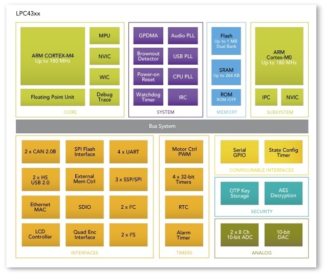
LPC43xx
The LPC43xx series represents a pivotal advancement in the LPC4000 family, introducing a dual-core architecture that combines an ARM Cortex-M4 processor with a Cortex-M0 coprocessor to enable efficient multitasking in embedded systems. This design allows the Cortex-M4, operating at up to 204 MHz with a floating-point unit (FPU), to manage computationally intensive tasks such as signal processing and control algorithms, while the Cortex-M0, also capable of up to 204 MHz, handles real-time input/output operations and peripheral management to ensure low-latency responses.[17] The series supports inter-core communication through shared SRAM acting as a mailbox mechanism and an event router for interrupt-based signaling, facilitating seamless code partitioning where complex application logic runs on the M4 and deterministic tasks on the M0. Memory resources in the LPC43xx are optimized for dual-core operation, featuring up to 1 MB of dual-bank flash memory that permits simultaneous read/write operations across banks, alongside up to 264 kB of SRAM distributed in multiple power-domain blocks for flexible allocation between cores. An external memory controller (EMC) further extends capabilities by interfacing with SDRAM, NAND flash, NOR flash, and static RAM, supporting bus widths up to 32 bits depending on the package.[17] This configuration bridges legacy systems requiring robust I/O handling with modern demands for higher performance, as evidenced by the series' integration of connectivity features like a high-speed USB 2.0 interface (480 Mbps) supporting host, device, and OTG modes with DMA, a 10/100 Mbps Ethernet MAC compliant with IEEE 1588 for precise timing, and up to two CAN 2.0B controllers for automotive and industrial networking.[17][18] Clocking in the LPC43xx is managed by an advanced phase-locked loop (PLL) system, including PLL0 for USB synchronization (14 kHz to 25 MHz input), PLL1 for main system clocks (up to 320 MHz internally before division to 204 MHz), and an audio-dedicated PLL, all fed by a 1-25 MHz crystal oscillator or a 12 MHz internal RC oscillator. This multi-domain clocking architecture allows independent frequency scaling for peripherals and cores, enhancing power efficiency in applications like motor control, industrial automation, and consumer electronics.[17] Introduced in 2011, the LPC43xx targeted scenarios needing partitioned code execution to optimize resource use without compromising real-time performance.[18]LPC40xx
The LPC40xx family consists of single-core Arm Cortex-M4-based microcontrollers developed by NXP Semiconductors for embedded applications emphasizing high integration, signal processing capabilities, and efficient power usage. These devices target general-purpose control, human-machine interfaces, and industrial automation, offering a balance of performance and peripheral support without the complexity of dual-core architectures. Introduced in 2012, the LPC40xx series provides scalable options for developers, with flash memory ranging from 64 KB to 512 KB and SRAM from 16 KB to 96 KB, enabling flexible code and data storage for real-time systems.[19][20] At the heart of the LPC40xx is a 32-bit Arm Cortex-M4 processor core operating at up to 120 MHz, incorporating digital signal processing instructions and, on select models, a single-precision floating-point unit (FPU) compliant with IEEE 754-2008 for accelerated mathematical operations in applications like motor control and sensor processing. Memory configuration supports in-system programming (ISP) and in-application programming (IAP) through UART0 or SPIFI interfaces, allowing field updates without specialized hardware. The family distinguishes itself through integrated peripherals tailored for display and analog interfacing, including a motor control PWM unit capable of generating precise waveforms for three-phase motor drives and a 12-bit successive approximation ADC with 8 multiplexed channels, achieving conversion rates up to 400 kSamples/s at full resolution. Higher-end variants also feature an LCD controller supporting STN and TFT panels up to 1024 × 768 resolution with 24-bit color depth.[19] Power efficiency is achieved via dynamic scaling across multiple modes—active, sleep, deep-sleep, power-down, and deep power-down—operating on a single 3.3 V supply (2.4 V to 3.6 V range). Typical active-mode current draw is approximately 56 mA at 120 MHz with peripherals enabled, equating to about 467 µA/MHz, while power-down mode reduces consumption to 280–600 µA, supporting battery-powered or energy-constrained designs. The LPC407x variants serve general-purpose needs with USB device/host support and up to 512 KB flash but lack Ethernet and LCD on lower models, whereas the LPC408x extends functionality with an integrated Ethernet MAC for networked applications, external memory controller (EMC), and FPU across the lineup, making it suitable for connectivity-focused prototyping and development.[19]LPC3000 Series
LPC32xx
The LPC32xx series, specifically the LPC32x0 family, represents NXP Semiconductors' early ARM9-based microcontrollers designed for embedded applications requiring a balance of high performance and low power consumption. These devices feature the ARM926EJ-S core, a 16/32-bit RISC processor with a 5-stage pipeline, Harvard architecture, Memory Management Unit (MMU), and DSP extensions for enhanced signal processing tasks. The core supports operation at frequencies up to 266 MHz, delivering approximately 220 MIPS of performance, and includes hardware-based Jazelle technology for direct execution of Java byte-code, enabling efficient Java applications without interpretation overhead. Additionally, an integrated Vector Floating Point (VFP) coprocessor accelerates floating-point computations, making it suitable for graphics and signal processing workloads.[21] Memory architecture in the LPC32xx emphasizes flexibility for multimedia and storage-intensive uses, with 32 kB of instruction cache and 32 kB of data cache to optimize core performance by reducing external memory access latency. The series provides a dedicated interface for SDR or DDR SDRAM, supporting 16- or 32-bit wide buses and capacities up to 512 Mbit (64 MB) per bank at speeds up to 133 MHz, allowing seamless integration of large dynamic memory pools. For non-volatile storage, dual NAND flash controllers—one for single-level cell (SLC) and one for multi-level cell (MLC) devices—enable direct connection to various flash sizes and configurations, with built-in error correction via Reed-Solomon encoding/decoding and DMA support to minimize CPU intervention during data transfers. On-chip SRAM ranges from 128 kB to 256 kB across variants, providing fast access for code and data.[21] Peripherals in the LPC32xx are oriented toward multimedia and connectivity, including a versatile LCD controller that drives STN or TFT panels with resolutions up to 1024 × 768 pixels, palette or direct color modes (up to 24-bit), and dedicated DMA for efficient frame buffer handling, ideal for display-intensive applications. A USB 2.0 full-speed OTG interface supports host, device, or OTG modes with an integrated OHCI-compliant host controller and dedicated PLL for 48 MHz operation, facilitating peripherals like storage devices or human-interface inputs. Other notable integrations include a 10/100 Ethernet MAC with DMA and hardware acceleration for checksums and frame filtering on select models (LPC3240/3250), multiple I²C, SPI, and UART interfaces, as well as a 10-bit ADC with touchscreen support. These features position the LPC32xx for consumer electronics, industrial controls, and medical devices requiring graphical interfaces and networked connectivity.[21][22] Clocking and power management employ a multi-PLL system, including a 397x PLL for precise RTC derivation, a USB PLL for stable 48 MHz, and an HCLK PLL for scalable peripheral clocks, allowing independent domain control to optimize power in dynamic workloads. The core operates at a supply voltage of 0.9 V to 1.39 V (typically 1.35 V for full speed), while I/O pads support 1.8 V, 3.0 V, or 3.3 V levels for broad compatibility, and EMC interfaces (for memory) range from 1.7 V to 3.6 V. Released around 2008, the LPC32xx series has become a legacy platform but remains relevant in legacy systems for its robust multimedia capabilities and Linux support via provided board support packages. As of 2025, the series is discontinued with limited availability under NXP's product longevity program.[21][22][23]LPC31xx
The LPC31xx series, part of NXP's LPC3000 family, consists of low-cost, power-efficient ARM9-based microcontrollers optimized for applications needing high-speed USB connectivity, external memory support, and battery-powered operation. Introduced in 2009 as a more energy-efficient alternative to the higher-performance LPC32xx series, these devices target industrial, consumer, and portable systems where compact design and low power are critical.[24] At the heart of the LPC31xx is the ARM926EJ-S processor core, operating at clock speeds of 180 MHz in base models like the LPC3130/3131 and up to 270 MHz in variants such as the LPC3141/3143, with support for dynamic voltage and frequency scaling to balance performance and energy use. The core includes a Memory Management Unit (MMU) for multitasking, along with separate 16 kB instruction and 16 kB data caches featuring 8-word line lengths to enhance execution efficiency from external memory.[25][26] Memory architecture emphasizes flexibility for storage-intensive tasks, with up to 192 kB of on-chip SRAM and a multi-port memory controller (MPMC) supporting up to 128 MB of external SDRAM or SRAM via an 8/16-bit interface. A dedicated NAND flash controller handles 8/16-bit devices with hardware 8-bit ECC for reliable data storage, commonly used in industrial firmware applications.[25][26] Key integrated peripherals include a secure digital host controller compatible with SD/MMC, SDHC, SDIO, and CE-ATA cards for removable storage, alongside two I²S interfaces for audio codec connectivity in portable devices. A battery-backed real-time clock (RTC) ensures timekeeping in low-power states, supporting applications like data logging.[25][27] Power management is a standout feature, with a 1.2 V core supply enabling ultra-low consumption: typical standby mode draws 1.75 mW, while deep sleep can reach as low as 50 µA, making the LPC31xx suitable for battery-operated industrial controls and consumer gadgets. Variants like the LPC313x focus on general industrial use, the LPC314x adds AES decryption and one-time programmable (OTP) memory for security, and the LPC315x incorporates a stereo audio codec with headphone amplifier for multimedia peripherals. As of 2025, the series is discontinued with limited availability under NXP's product longevity program.[25][27][23]LPC2000 Series
The LPC2000 series, introduced in the mid-2000s, is now considered legacy by NXP as of 2025, with varying availability across devices.[28]LPC24xx and LPC23xx
The LPC24xx and LPC23xx series represent higher-end models within the LPC2000 family of microcontrollers, designed for demanding embedded applications requiring advanced connectivity and integration. These devices are built around the ARM7TDMI-S 16-bit/32-bit RISC processor core, which operates at speeds up to 72 MHz, providing efficient performance for real-time tasks while maintaining low power consumption.[29][30] The architecture supports real-time emulation and debugging interfaces, such as EmbeddedICE, enabling seamless development for complex systems.[29] Memory configurations in the LPC23xx series typically include 128 kB to 512 kB of on-chip flash memory for program storage, paired with 16 kB to 64 kB of SRAM for data handling, including dedicated portions for peripherals like Ethernet and USB.[29] The LPC24xx series extends this with 256 kB to 512 kB flash and up to 96 kB total SRAM, incorporating additional general-purpose and DMA-accessible RAM blocks to support more intensive multitasking.[30] Both series feature In-System Programming (ISP) and In-Application Programming (IAP) capabilities for the flash, allowing field updates without specialized hardware.[29][30] Key peripherals emphasize connectivity and interface versatility. Select models in the LPC23xx series integrate a 10/100 Ethernet MAC with DMA support for networked applications, two CAN 2.0B controllers for robust industrial communication, and a full-speed USB 2.0 device controller with 4 kB of dedicated endpoint RAM.[29] Building on this, the LPC24xx adds an LCD controller capable of driving STN and TFT panels up to 1024 × 768 resolution, an external memory controller for interfacing with SDRAM or other devices, and enhanced motor control timers with up to 10 compare outputs for PWM generation in automation tasks.[30] Both series include four 32-bit timers with capture/compare functions, multiple UARTs, SSP/SPI, I²C, and I²S interfaces, along with a 10-bit ADC and DAC for analog signal processing.[29][30] Clocking is managed via an on-chip PLL that multiplies the input oscillator frequency (from 32 kHz to 25 MHz) to achieve the full 72 MHz CPU speed, with options for USB and Ethernet clocking derived from the same source.[29][30] Brown-out detection circuitry monitors supply voltage with configurable thresholds—typically 2.95 V for interrupt and 2.65 V for reset—ensuring reliable operation in power-unstable environments.[30] Introduced in 2006–2007, these series gained popularity in USB-intensive applications such as printers, point-of-sale terminals, and industrial controllers due to their balanced integration of host/device USB functionality with networking capabilities.[31][32]LPC21xx and LPC22xx
The LPC21xx and LPC22xx series represent early members of NXP's LPC2000 family of ARM-based microcontrollers, designed for cost-effective embedded applications requiring moderate processing power. These devices are built around the ARM7TDMI-S core, a 16/32-bit RISC processor operating at up to 60 MHz for flash-based variants or 75 MHz for flashless models.[33] The LPC21xx subfamily targets simpler designs with on-chip flash memory ranging from 32 kB to 256 kB and SRAM from 8 kB to 32 kB, while the LPC22xx extends this with support for external memory interfaces, offering up to 256 kB flash or flashless configurations paired with 16 kB to 64 kB SRAM.[33] Both support In-System Programming (ISP) and In-Application Programming (IAP) via a built-in bootloader, enabling field updates without specialized hardware.[34] Key integrated peripherals emphasize versatile I/O for control tasks, including two UARTs for serial communication, one I²C interface operating up to 400 kbit/s in master/slave modes, and two SPI ports for 8- to 16-bit data transfers.[33] A 10-bit ADC with up to 8 channels (depending on package) handles analog inputs, complemented by a PWM unit providing six outputs suitable for motor control and timing applications.[34] These features make the series ideal for foundational embedded systems without needing external components for basic interfacing. Power management is optimized for low-energy operation at 3.3 V nominal supply (3.0 V to 3.6 V for I/O, 1.8 V core), with active-mode consumption around 40 mA at 60 MHz—equating to less than 1 mA/MHz—and power-down mode drawing under 10 µA at room temperature.[34] Reliability is enhanced by an integrated watchdog timer for system monitoring and brown-out detection to prevent operation during voltage dips.[33] Introduced between 2004 and 2005, the LPC21xx and LPC22xx series gained popularity in educational settings, such as with the LPC2103-based development boards for teaching ARM architecture and peripherals, and in simple control applications like industrial sensors and consumer devices.[35][36]LPC1000 Series
LPC18xx and LPC17xx
The LPC17xx series represents NXP's high-performance ARM Cortex-M3-based microcontrollers designed for embedded applications requiring robust connectivity and processing capabilities. These devices feature a 32-bit ARM Cortex-M3 core operating at up to 100 MHz for most variants (LPC176x) or 120 MHz for the LPC1769, enabling efficient execution of complex control algorithms.[37] Memory configurations include 128 KB to 512 KB of on-chip flash and 32 KB to 64 KB of SRAM, with some models supporting an external memory bus for additional expansion.[37] Key integrated peripherals emphasize industrial and networking demands, such as two CAN 2.0B controllers for automotive and control networks, USB 2.0 OTG/full-speed host/device interfaces for connectivity, and Ethernet MAC (10/100 Mbps) on select models like the LPC1768 for networked applications.[37] Clocking is managed via a high-frequency PLL supporting up to 120 MHz from a 1-25 MHz crystal oscillator or 4 MHz internal RC, ensuring stable operation in demanding environments.[37] Introduced in 2008, the LPC17xx series targets applications like motor control, eMetering, and industrial networking.[38] These devices are included in NXP's 15-year product longevity program, ensuring availability until at least 2038.[39] Building on the LPC17xx foundation, the LPC18xx series advances performance with enhanced speed and memory for more intensive tasks such as robotics and advanced networking. The ARM Cortex-M3 core runs at up to 180 MHz, providing superior computational throughput compared to earlier models.[40] Memory options scale to 256 KB–1 MB of dual-bank flash, 64–136 KB of SRAM, and 16 KB of EEPROM, complemented by an external bus interface (EBI) supporting up to 1 GB of external memory for flexible system expansion.[40] Peripherals are optimized for high-speed integration, including 10/100 Ethernet MAC with IEEE 1588 timing support, two high-speed USB 2.0 interfaces (one OTG), two CAN 2.0B controllers, and a Quad SPI Flash Interface (SPIFI) enabling up to 52 MB/s data rates for rapid code execution from external storage.[40] Clock generation utilizes three PLLs and a 1–25 MHz crystal oscillator to achieve the 180 MHz system clock, with a 12 MHz internal RC for initialization.[40] Announced in 2010, the LPC18xx series suits high-demand control systems in industrial automation, RFID readers, and networked consumer devices.[41] These devices are included in NXP's product longevity program.[23]| Feature | LPC17xx | LPC18xx |
|---|---|---|
| Core Clock | Up to 120 MHz | Up to 180 MHz |
| Flash Memory | 128–512 KB | 256 KB–1 MB |
| SRAM | 32–64 KB | 64–136 KB |
| Key Peripherals | 2x CAN, USB OTG, Ethernet (select) | 2x CAN, 2x HS USB, Ethernet, Quad SPI |
| External Bus | Limited (select models) | EBI up to 1 GB |
| Target Applications | Motor control, eMetering | Robotics, advanced networking |