
Community hub
Recent from talks
Contribute something
Nothing was collected or created yet.
Transputer
View on WikipediaThis article has multiple issues. Please help improve it or discuss these issues on the talk page. (Learn how and when to remove these messages)
|

The transputer is a series of pioneering microprocessors from the 1980s, intended for parallel computing. To support this, each transputer had its own integrated memory and serial communication links to exchange data with other transputers. They were designed and produced by Inmos, a semiconductor company based in Bristol, United Kingdom.[1]
For some time in the late 1980s, many[2] considered the transputer to be the next great design for the future of computing. While the transputer did not achieve this expectation, the transputer architecture was highly influential in provoking new ideas in computer architecture, several of which have re-emerged in different forms in modern systems.[3]
Background
[edit]In the early 1980s, conventional central processing units (CPUs) appeared to have reached a performance limit. Up to that time, manufacturing difficulties limited the amount of circuitry that could fit on a chip. Continued improvements in the fabrication process had largely removed this restriction. Within a decade, chips could hold more circuitry than the designers knew how to use. Traditional complex instruction set computer (CISC) designs were reaching a performance plateau, and it wasn't clear it could be overcome.[4]
It seemed that the only way forward was to increase the use of parallelism, the use of several CPUs that would work together to solve several tasks at the same time. This depended on such machines being able to run several tasks at once, a process termed multitasking. This had generally been too difficult for prior microprocessor designs to handle, but more recent designs were able to accomplish it effectively. It was clear that in the future, this would be a feature of all operating systems (OSs).
A side effect of most multitasking design is that it often also allows the processes to be run on physically different CPUs, in which case it is termed multiprocessing. A low-cost CPU built for multiprocessing could allow the speed of a machine to be raised by adding more CPUs, potentially far more cheaply than by using one faster CPU design.
The first transputer designs were due to computer scientist David May and telecommunications consultant Robert Milne. In 1990, May received an Honorary DSc from University of Southampton, followed in 1991 by his election as a Fellow of The Royal Society and the award of the Patterson Medal of the Institute of Physics in 1992. Tony Fuge, then a leading engineer at Inmos, was awarded the Prince Philip Designers Prize in 1987 for his work on the T414 transputer.[5]
Design
[edit]The transputer was the first general purpose microprocessor designed specifically to be used in parallel computing systems. The goal was to produce a family of chips ranging in power and cost that could be wired together to form a complete parallel computer. The name, from "transistor" and "computer",[6] was selected to indicate the role the individual transputers would play: numbers of them would be used as basic building blocks in a larger integrated system, just as transistors had been used in earlier designs.
Originally the plan was to make the transputer cost only a few dollars per unit. Inmos saw them being used for practically everything, from operating as the main CPU for a computer to acting as a channel controller for disk drives in the same machine. In a traditional machine, the processing capability of a disk controller, for instance, would be idle when the disk was not being accessed. In contrast, in a transputer system, spare cycles on any of these transputers could be used for other tasks, greatly increasing the overall performance of the machines.
The transputer had large on-chip memory, making it essentially a processor-in-memory. Even one transputer would have all the circuitry needed to work by itself, a feature more commonly associated with microcontrollers. The intent was to allow transputers to be connected together as easily as possible, with no need for a complex bus, or motherboard. Power and a simple clock signal had to be supplied, but little else: random-access memory (RAM), a RAM controller, bus support and even a real-time operating system (RTOS) were all built in. In this way, the last of the transputers were single Reusable Micro Cores (RMC) in the then emerging SoC market.
Architecture
[edit]The original transputer used a very simple and rather unusual architecture to achieve a high performance in a small area. It used microcode as the main method to control the data path, but unlike other designs of the time, many instructions took only one cycle to execute. Instruction opcodes were used as the entry points to the microcode read-only memory (ROM) and the outputs from the ROM were fed directly to the data path. For multi-cycle instructions, while the data path was performing the first cycle, the microcode decoded four possible options for the second cycle. The decision as to which of these options would actually be used could be made near the end of the first cycle. This allowed for very fast operation while keeping the architecture generic.[7]
The clock rate of 20 MHz was quite high for the era and the designers were very concerned about the practicality of distributing such a fast clock signal on a board. A slower external clock of 5 MHz was used, and this was multiplied up to the needed internal frequency using a phase-locked loop (PLL). The internal clock actually had four non-overlapping phases and designers were free to use whichever combination of these they wanted, so it could be argued that the transputer actually ran at 80 MHz. Dynamic logic was used in many parts of the design to reduce area and increase speed. Unfortunately, these methods are difficult to combine with automatic test pattern generation scan testing so they fell out of favour for later designs.
Prentice-Hall published a book[8] on the general principles of the transputer.
Links
[edit]The basic design of the transputer included serial links known as "os-link"s[9][10] that allowed it to communicate with up to four other transputers, each at 5, 10, or 20 Mbit/s – which was very fast for the 1980s. Any number of transputers could be connected together over links (which could run tens of metres over differential wiring) to form one computing farm. A hypothetical desktop machine might have two of the "low end" transputers handling input/output (I/O) tasks on some of their serial lines (hooked up to appropriate hardware) while they talked to one of their larger cousins acting as a CPU on another.
There were limits to the size of a system that could be built in this fashion. Since each transputer was linked to another in a fixed point-to-point layout, sending messages to a more distant transputer required that messages be relayed by each chip in the line. This introduced a delay with every "hop" over a link, leading to long delays on large nets. To solve this problem Inmos also provided a zero-delay switch that connected up to 32 transputers (or switches) into even larger networks.
Booting
[edit]Transputers could boot from memory, as is the case for most computers, but could also be booted over its network links. A special pin on the chips, BootFromROM, indicated which method it should use. If BootFromROM was asserted when the chip was reset, it would begin processing at the instruction two bytes from the top of memory, which was normally used to perform a backward jump into the boot code. If this pin was not asserted, the chip would instead wait for bytes to be received on any network link. The first byte to be received was the length of the code to follow. Following bytes were copied into low memory and then jumped into once that number of bytes had been received.
The general concept for the system was to have one transputer act as the central authority for booting a system containing a number of connected transputers. The selected transputer would have the BootFromROM permanently asserted, which would cause it to begin running a booter process from ROM on startup. The other transputers would have the BootFromROM tied low, and would simply wait. The loader would boot the central transputer, which would then begin sending boot code to the other transputers in the network, and could customize the code sent to each one, for instance, sending a device driver to the transputer connected to the hard drives.
The system also included the 'special' code lengths of 0 and 1 which were reserved for PEEK and POKE. This allowed inspection and changing of RAM in an unbooted transputer. After a peek, followed by a memory address, or a poke, with an address and single word of data, the transputer would return to waiting for a bootstrap. This mechanism was generally used for debugging.
Scheduler
[edit]Added circuitry scheduled traffic over the links. Processes waiting for communications would automatically pause while the networking circuitry finished its reads or writes. Other processes running on the transputer would then be given that processing time. It included two priority levels to improve real-time and multiprocessor operation. The same logical system was used to communicate between programs running on one transputer, implemented as virtual network links in memory. So programs asking for any input or output automatically paused while the operation completed, a task that normally required an operating system to handle as the arbiter of hardware. Operating systems on the transputer did not need to handle scheduling; the chip could be considered to have an OS inside it.
Instruction set
[edit]To include all this function on one chip, the transputer's core logic was simpler than most CPUs. While some have called it reduced instruction set computer (RISC) due to its rather sparse nature, and because that was then a desirable marketing buzzword, it was heavily microcoded, had a limited register set, and complex memory-to-memory instructions, all of which place it firmly in the CISC camp. Unlike register-heavy load/store RISC CPUs, the transputer had only three data registers, which behaved as a stack. In addition a workspace pointer pointed to a conventional memory stack, easily accessible via the instructions Load Local and Store Local. This allowed for very fast context switching by simply changing the workspace pointer to the memory used by another process (a method used in a number of contemporary designs, such as the TMS9900). The three register stack contents were not preserved past certain instructions, like Jump, when the transputer could do a context switch.
The transputer instruction set consisted of 8-bit instructions assembled from opcode and operand nibbles. The upper nibble contained the 16 possible primary instruction codes, making it one of the very few commercialized minimal instruction set computers. The lower nibble contained the one immediate constant operand, commonly used as an offset relative to the workspace (memory stack) pointer. Two prefix instructions allowed construction of larger constants by prepending their lower nibbles to the operands of following instructions. Further instructions were supported via the instruction code Operate (Opr), which decoded the constant operand as an extended zero-operand opcode, providing for almost endless and easy instruction set expansion as newer implementations of the transputer were introduced.
The 16 'primary' one-operand instructions were:
| Mnemonic | Description |
|---|---|
| J | Jump – add immediate operand to instruction pointer |
| LDLP | Load local pointer – load a workspace-relative pointer onto the top of the register stack |
| PFIX | Prefix – general way to increase lower nibble of following primary instruction |
| LDNL | Load non-local – load a value offset from address at top of stack |
| LDC | Load constant – load constant operand onto the top of the register stack |
| LDNLP | Load non-local pointer – load address, offset from top of stack |
| NFIX | Negative prefix – general way to negate (and possibly increase) lower nibble |
| LDL | Load local – load value offset from workspace |
| ADC | Add constant – add constant operand to top of register stack |
| CALL | Subroutine call – push instruction pointer and jump |
| CJ | Conditional jump – depending on value at top of register stack |
| AJW | Adjust workspace – add operand to workspace pointer |
| EQC | Equals constant – test if top of register stack equals constant operand |
| STL | Store local – store at constant offset from workspace |
| STNL | Store non-local – store at address offset from top of stack |
| OPR | Operate – general way to extend instruction set |
All these instructions take a constant, representing an offset or an arithmetic constant. If this constant was less than 16, all these instructions coded to one byte.
The first 16 'secondary' zero-operand instructions (using the OPR primary instruction) were:
| Mnemonic | Description |
|---|---|
| REV | Reverse – swap two top items of register stack |
| LB | Load byte |
| BSUB | Byte subscript |
| ENDP | End process |
| DIFF | Difference |
| ADD | Add |
| GCALL | General call – swap top of stack and instruction pointer |
| IN | Input – receive message |
| PROD | Product |
| GT | Greater than – the only comparison instruction |
| WSUB | Word subscript |
| OUT | Output – send message |
| SUB | Subtract |
| STARTP | Start process |
| OUTBYTE | Output byte – send one-byte message |
| OUTWORD | Output word – send one-word message |
Development
[edit]To provide an easy means of prototyping, constructing and configuring multiple-transputer systems, Inmos introduced the TRAM (TRAnsputer Module) standard in 1987. A TRAM was essentially a building block daughterboard comprising a transputer and, optionally, external memory and/or peripheral devices, with simple standardised connectors providing power, transputer links, clock and system signals. Various sizes of TRAM were defined, from the basic Size 1 TRAM (3.66 in by 1.05 in) up to Size 8 (3.66 in by 8.75 in). Inmos produced a range of TRAM motherboards for various host buses such as Industry Standard Architecture (ISA), MicroChannel, or VMEbus. TRAM links operate at 10 Mbit/s or 20 Mbit/s.[11]
Software
[edit]Transputers were intended to be programmed using the programming language occam, based on the communicating sequential processes (CSP) process calculus.[12] The transputer was built to run occam specifically, more than contemporary CISC designs were built to run languages like Pascal or C. Occam supported concurrency and channel-based inter-process or inter-processor communication as a fundamental part of the language. With the parallelism and communications built into the chip and the language interacting with it directly, writing code for things like device controllers became a triviality[citation needed]; even the most basic[weasel words] code could watch the serial ports for I/O, and would automatically sleep when there was no data.
The initial Occam development environment for the transputer was the Inmos D700 Transputer Development System (TDS). This was an unorthodox integrated development environment incorporating an editor, compiler, linker and (post-mortem) debugger. The TDS was a transputer application written in Occam. The TDS text editor was notable in that it was a folding editor, allowing blocks of code to be hidden and revealed, to make the structure of the code more apparent. Unfortunately, the combination of an unfamiliar programming language and equally unfamiliar development environment did nothing for the early popularity of the transputer.[citation needed] Later, Inmos would release more conventional Occam cross-compilers, the Occam 2 Toolsets.
Implementations of more mainstream programming languages, such as C, FORTRAN, Ada, Forth, and Pascal were also later[when?] released by both Inmos and third-party vendors[who?][citation needed]. These usually[weasel words] included language extensions or libraries providing, in a less elegant way[citation needed], Occam-like concurrency and channel-based communication.[citation needed]
The transputer's lack of support for virtual memory inhibited the porting of mainstream variants of the Unix operating system, though ports of Unix-like operating systems (such as Minix and Idris from Whitesmiths) were produced[citation needed]. An advanced Unix-like distributed operating system, Helios, was also designed specifically for multi-transputer systems by Perihelion Software.[citation needed]
Implementations
[edit]The first transputers were announced in 1983 and released in 1984.
In keeping with their role as microcontroller-like devices, they included on-board RAM and a built-in RAM controller which enabled more memory to be added with no added hardware. Unlike other designs, transputers did not include I/O lines: these were to be added with hardware attached to the existing serial links. There was one 'Event' line, similar to a conventional processor's interrupt line. Treated as a channel, a program could 'input' from the event channel, and proceed only after the event line was asserted.
All transputers ran from an external 5 MHz clock input; this was multiplied to provide the processor clock.
The transputer did not include a memory management unit (MMU) or a virtual memory system.
Transputer variants (except the cancelled T9000) can be categorised into three groups: the 16-bit T2 series, the 32-bit T4 series, and the 32-bit T8 series with 64-bit IEEE 754 floating-point support.
T2: 16-bit
[edit]
The prototype 16-bit transputer was the S43, which lacked the scheduler and DMA-controlled block transfer on the links. At launch, the T212 and M212 (the latter with an on-board disk controller) were the 16-bit offerings. The T212 was available in 17.5 and 20 MHz processor clock speed ratings. The T212 was superseded by the T222, with on-chip RAM expanded from 2 KB to 4 KB, and, later, the T225. This added debugging-breakpoint support (by extending the instruction "J 0") plus some extra instructions from the T800 instruction set. Both the T222 and T225 ran at 20 MHz.
T4: 32-bit
[edit]
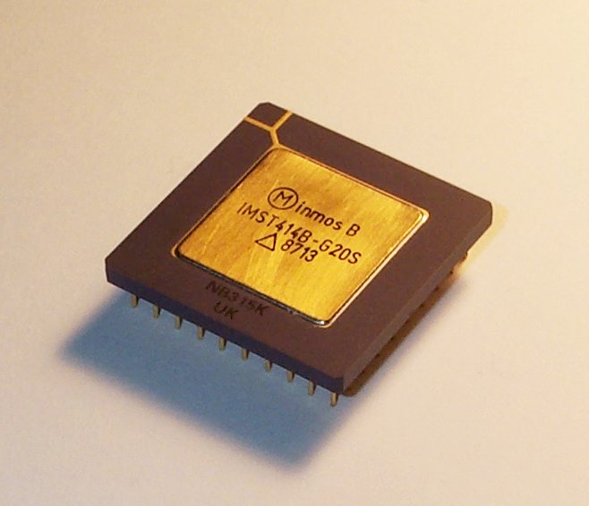
Launched in October 1985, the T414 employed the equivalent of 900,000 transistors and was fabricated with a 1.5 micrometre feature size. It was a 32-bit design, able to process 32-bit units of data and to address up to 4 GB of main memory.[13] Originally, the first 32-bit variant was to be the T424, but fabrication difficulties meant that this was redesigned as the T414 with 2 KB on-board RAM instead of the intended 4 KB. The T414 was available in 15 and 20 MHz varieties. The RAM was later reinstated to 4 KB on the T425 (in 20, 25, and 30 MHz varieties), which also added the J 0 breakpoint support and extra T800 instructions. The T400, released in September 1989, was a low-cost 20 MHz T425 derivative with 2 KB and two instead of four links, intended for the embedded systems market.
T8: floating point
[edit]
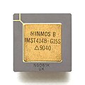
The second-generation T800 transputer, introduced in 1987, had an extended instruction set. The most important addition was a 64-bit floating-point unit (FPU) and three added registers for floating point, implementing the IEEE 754-1985 floating point standard. It also had 4 KB of on-board RAM and was available in 20 or 25 MHz versions. Breakpoint support was added in the later T801 and T805, the former featuring separate address and data buses to improve performance. The T805 was also later available as a 30 MHz part.
An enhanced T810 was planned, which would have had more RAM, more and faster links, extra instructions, and improved microcode, but this was cancelled around 1990.
Inmos also produced a variety of support chips for the transputer processors, such as the C004 32-way link switch and the C011 and C012 "link adapters" which allowed transputer links to be interfaced to an 8-bit data bus.
T400
[edit]Part of the original Inmos strategy was to make CPUs so small and cheap that they could be combined with other logic in one device. Although a system on a chip (SoC) as they are commonly termed, are ubiquitous now, the concept was almost unheard of back in the early 1980s. Two projects were started in around 1983, the M212 and the TV-toy. The M212 was based on a standard T212 core with the addition of a disk controller for the ST 506 and ST 412 Shugart standards. TV-toy was to be the basis for a video game console and was joint project between Inmos and Sinclair Research.
The links in the T212 and T414/T424 transputers had hardware DMA engines so that transfers could happen in parallel with execution of other processes. A variant of the design, termed the T400, not to be confused with a later transputer of the same name, was designed where the CPU handled these transfers. This reduced the size of the device considerably since 4 link engines were approximately the same size as the whole CPU. The T400 was intended to be used as a core in what were then called systems on silicon (SOS) devices, now termed and better known as system on a chip (SoC). It was this design that was to form part of TV-toy. The project was canceled in 1985.
T100
[edit]Although the prior SoC projects had had only limited success (the M212 was sold for a time), many designers still firmly believed in the concept and in 1987, a new project, the T100 was started which combined an 8-bit version of the transputer CPU with configurable logic based on state machines. The transputer instruction set is based on 8-bit instructions and can easily be used with any word size which is a multiple of 8 bits. The target market for the T100 was to be bus controllers such as Futurebus, and an upgrade for the standard link adapters (C011 etc.). The project was stopped when the T840 (later to become the basis of the T9000) was started.
- T2, T4, and T8 series transputers
-
 Inmos T212, PREQUAL
 -
 Inmos T222, PREQUAL
 -
 STMicroelectronics IMST225 (Inmos T225)
 -
 Inmos T400
 -
 Inmos T414
 -
 Inmos T425
 -
 Inmos T800, PREQUAL
 -
 STMicroelectronics IMST805 (Inmos T805)


TPCORE
[edit]TPCORE is an implementation of the transputer, including the os-links, that runs in a field-programmable gate array (FPGA).[9][14]
T9000
[edit]
Inmos improved on the performance of the T8 series transputers with the introduction of the T9000 (code-named H1 during development). The T9000 shared most features with the T800, but moved several pieces of the design into hardware and added several features for superscalar support. Unlike the earlier models, the T9000 had a true 16 KB high-speed cache (using random replacement) instead of RAM, but also allowed it to be used as memory and included MMU-like functionality to handle all of this (termed the PMI). For more speed the T9000 cached the top 32 locations of the stack, instead of three as in earlier versions.

The T9000 used a five-stage pipeline for even more speed. An interesting addition was the grouper[15] which would collect instructions out of the cache and group them into larger packages of up to 8 bytes to feed the pipeline faster. Groups then completed in one cycle, as if they were single larger instructions working on a faster CPU.
The link system was upgraded to a new 100 MHz mode, but unlike the prior systems, the links were no longer downwardly compatible. This new packet-based link protocol was called DS-Link,[16] and later formed the basis of the IEEE 1355 serial interconnect standard. The T9000 also added link routing hardware called the VCP (Virtual Channel Processor) which changed the links from point-to-point to a true network, allowing for the creation of any number of virtual channels on the links. This meant programs no longer had to be aware of the physical layout of the connections. A range of DS-Link support chips were also developed, including the C104 32-way crossbar switch, and the C101 link adapter.
Long delays in the T9000's development meant that the faster load/store designs were already outperforming it by the time it was to be released. It consistently failed to reach its own performance goal of beating the T800 by a factor of ten. When the project was finally cancelled it was still achieving only about 36 MIPS at 50 MHz. The production delays gave rise to the quip that the best host architecture for a T9000 was an overhead projector.
This was too much for Inmos, which did not have the funding needed to continue development. By this time, the company had been sold to SGS-Thomson (now STMicroelectronics), whose focus was the embedded systems market, and eventually the T9000 project was abandoned. However, a comprehensively redesigned 32-bit transputer intended for embedded applications, the ST20 series, was later produced, using some technology developed for the T9000. The ST20 core was incorporated into chipsets for set-top box and Global Positioning System (GPS) applications.
ST20
[edit]Although not strictly a transputer, the ST20 was heavily influenced by the T4 and T9 and formed the basis of the T450, which was arguably the last of the transputers. The mission of the ST20 was to be a reusable core in the then emerging SoC market. The original name of the ST20 was the Reusable Micro Core (RMC). The architecture was loosely based on the original T4 architecture with a microcode-controlled data path. However, it was a full redesign, using VHDL as the design language and with an optimized (and rewritten) microcode compiler. The project was conceived as early as 1990 when it was realized that the T9 would be too big for many applications. Actual design work started in mid-1992. Several trial designs were done, ranging from a very simple RISC-style CPU with complex instructions implemented in software via traps to a rather complex superscalar design similar in concept to the Tomasulo algorithm. The final design looked very similar to the original T4 core although some simple instruction grouping and a workspace cache were added to help with performance.
Adoption
[edit]While the transputer was simple but powerful compared to many contemporary designs, it never came close to meeting its goal of being used universally in both CPU and microcontroller roles. In the microcontroller market, the market was dominated by 8-bit machines where cost was the most serious consideration. Here, even the T2s were too powerful and costly for most users.
In the computer desktop and workstation field, the transputer was fairly fast (operating at about 10 million instructions per second (MIPS) at 20 MHz). This was excellent performance for the early 1980s, but by the time the floating-point unit (FPU) equipped T800 was shipping, other RISC designs had surpassed it. This could have been mitigated to a large extent if machines had used multiple transputers as planned, but T800s cost about $400 each when introduced, which meant a poor price/performance ratio. Few transputer-based workstation systems were designed; the most notable likely being the Atari Transputer Workstation.
The transputer was more successful in the field of massively parallel computing, where several vendors produced transputer-based systems in the late 1980s. These included Meiko Scientific (founded by ex-Inmos employees), Floating Point Systems, Parsytec,[17] and Parsys. Several British academic institutions founded research activities in the application of transputer-based parallel systems, including Bristol Polytechnic's Bristol Transputer Centre and the University of Edinburgh's Edinburgh Concurrent Supercomputer Project. Also, the Data Acquisition and Second Level Trigger systems of the High Energy Physics ZEUS Experiment for the Hadron Elektron Ring Anlage (HERA) collider at DESY was based on a network of over 300 synchronously clocked transputers divided into several subsystems. These controlled both the readout of the custom detector electronics and ran reconstruction algorithms for physics event selection.
The parallel processing abilities of the transputer were put to use commercially for image processing by the world's largest printing company, RR Donnelley & Sons, in the early 1990s. The ability to quickly transform digital images in preparation for print gave the firm a significant edge over their competitors. This development was led by Michael Bengtson in the RR Donnelley Technology Center. Within a few years, the processing ability of even desktop computers ended the need for custom multi-processing systems for the firm.[citation needed]
The German company Jäger Messtechnik used transputers for their early ADwin real-time data acquisition and control products.[18]
A French company built the Archipel Volvox Supercomputer with up to 144 T800 and T400 Transputers. It was controlled by a Silicon Graphics Indigo2 running UNIX and a special card that interfaced to the Volvox backplanes.
Transputers also found use in protocol analysers such as the Siemens/Tektronix K1103 and in military applications where the array architecture suited applications such as radar and the serial links (that were high speed in the 1980s) served well to save cost and weight in sub-system communications.
The transputer also appeared in products related to virtual reality such as the ProVision 100 system made by Division Limited of Bristol, featuring a combination of Intel i860, 80486/33 and Toshiba HSP processors, together with T805 or T425 transputers, implementing a rendering engine that could then be accessed as a server by PC, Sun SPARCstation or VAX systems.[19][20]
Myriade, a European miniaturized satellite platform developed by Astrium Satellites and CNES and used by satellites such as the Picard, is based on the T805 yielding around 4 MIPS and is scheduled to stay in production until about 2015.[21][22]
The asynchronous operation of the communications and computation allowed the development of asynchronous algorithms, such as Bane's "Asychronous Polynomial Zero Finding" algorithm.[23] The field of asynchronous algorithms, and the asynchronous implementation of current algorithms, is likely to play a key role in the move to exascale computing.
The High Energy Transient Explorer 2 (HETE-2) spacecraft used 4× T805 transputers and 8× DSP56001 yielding about 100 million instructions per second (MIPS) of performance.[24]
Legacy
[edit]Growing internal parallelism has been one driving force behind improvements in conventional CPU designs. Instead of explicit thread-level parallelism (as is used in the transputer), CPU designs exploited implicit parallelism at the instruction-level, inspecting code sequences for data dependencies and issuing multiple independent instructions to different execution units. This is termed superscalar processing. Superscalar processors are suited for optimising the execution of sequentially constructed fragments of code. The combination of superscalar processing and speculative execution delivered a tangible performance increase on existing bodies of code – which were mostly written in Pascal, Fortran, C and C++. Given these substantial and regular performance improvements to existing code there was little incentive to rewrite software in languages or coding styles which expose more task-level parallelism.
Nevertheless, the model of cooperating concurrent processors can still be found in cluster computing systems that dominate supercomputer design in the 21st century. Unlike the transputer architecture, the processing units in these systems typically use superscalar CPUs with access to substantial amounts of memory and disk storage, running conventional operating systems and network interfaces. Resulting from the more complex nodes, the software architecture used for coordinating the parallelism in such systems is typically far more heavyweight than in the transputer architecture.
The fundamental transputer motive remains, yet was masked for over 20 years by the repeated doubling of transistor counts. Inevitably, microprocessor designers finally ran out of uses for the greater physical resources, almost at the same time when technology scaling began to hit its limits. Power consumption, and thus heat dissipation needs, render further clock rate increases unfeasible. These factors led the industry towards solutions little different in essence from those proposed by Inmos.
Some of the most powerful supercomputers in the world, based on designs from Columbia University and built as IBM Blue Gene, are real-world incarnations of the transputer dream. They are vast assemblies of identical, relatively low-performance SoCs.
Recent trends have also tried to solve the transistor dilemma in ways that would have been too futuristic even for Inmos. On top of adding components to the CPU die and placing multiple dies in one system, modern processors increasingly place multiple cores in one die. The transputer designers struggled to fit even one core into its transistor budget. Today designers, working with a 1000-fold increase in transistor densities, can now typically place many. One of the most recent commercial developments has emerged from the firm XMOS, which has developed a family of embedded multi-core multi-threaded processors which resonate strongly with the transputer and Inmos. There is an emerging class of multicore/manycore processors taking the approach of a network on a chip (NoC), such as the Cell processor, Adapteva Epiphany architecture, Tilera, etc.
The transputer and Inmos helped establish Bristol, UK, as a hub for microelectronic design and innovation.
See also
[edit]References
[edit]- ^ Allen Kent, James G. Williams (eds.) (1998) "Encyclopedia of Computer Science and Technology", ISBN 0-8247-2292-2, "The Transputer Family of Products", by Hamid R. Arabnia.
- ^ Hey, Anthony J. G. (1990-01-01). "Supercomputing with transputers---past, present and future". Proceedings of the 4th international conference on Supercomputing - ICS '90. New York, NY, USA: ACM. pp. 479–489. doi:10.1145/77726.255192. ISBN 0897913698. S2CID 8612995.
- ^ Stoker, & White, A. . (2000). Mechatronic cine-film copying using transputer control. Mechatronics (Oxford), 10(7), 773–807. https://doi.org/10.1016/S0957-4158(99)00043-4
- ^ Fuller, Samuel H. & Millett, Lynette I., Editors (2011). The Future of Computing Performance, CSTB, National Academic Press, p. 84. ISBN 978-0-309-15951-7 Retrieved on November 2, 2016.
- ^ "The Prince Philip Designers Prize". The Design Council. Retrieved 2019-12-01.
- ^ Barron, Iann M. (1978). D. Aspinall (ed.). "The Transputer". The Microprocessor and Its Application: An Advanced Course. Cambridge University Press: 343. ISBN 0-521-22241-9. Retrieved 2009-05-18.
- ^ Stakem, Patrick H. The Hardware and Software Architecture of the Transputer, 2011, PRB Publishing, ASIN B004OYTS1K
- ^ Transputer Reference Manual (PDF). Prentice-Hall. 1988. ISBN 0-13-929001-X. Archived (PDF) from the original on 2022-10-09.
- ^ a b Kazuto Tanaka; Satoshi Iwanami; Takeshi Yamakawa; Chikara Fukunaga; Kazuto Matsui; Takashi Yoshida. "The Design and Performance of SpaceWire Router-network using CSP". p. 2.
- ^ "High-Performance Computing and Networking: International Conference and Exhibition, Amsterdam, the Netherlands, April 21-23, 1998 Proceedings". B C O'Neill; G Coulson; K L Wong; R Hotchkiss; J H Ng; S Clark; and P D Thomas. "An Interface Device to Support a Distributed Parallel System for the StrongARM Microprocessor". p. 1031.
- ^ "Inmos Technical Note 29: Dual-In-Line Transputer Modules (TRAMs)". Transputer.net. 2008-07-04. Retrieved 2013-10-12.
- ^ Borger, & Durdanovic, I. (1996). Correctness of compiling Occam to transputer code. Computer Journal, 39(1), 52–92. https://doi.org/10.1093/comjnl/39.1.52
- ^ Anning, Nick; Hebditch, David (1986-03-20). "New chip displays its powers". New Scientist. pp. 43–46. Retrieved 2022-06-22.
- ^ "Communicating Process Architectures 2004". p. 361. Makoto Tanaka; Naoya Fukuchi; Yutaka Ooki; and Chikara Fukunaga. "Design of a Transputer Core and its implementation in an FPGA". 2004.
- ^ Inmos T9000 CPU patent, "US patent 5742783",
- ^ Inmos DS Link patent, "Communication Interface US patent 5341371"
- ^ Harald W. Wabnig (20–22 September 1993). Virtual Channels for Deadlock-Free Communication in Transputer Networks. 1993 World Transputer Congress. Aachen, Germany. p. 1047. ISBN 9789051991406.
- ^ "ADwin Fast Real-Time Automation System" (PDF). Archived from the original (PDF) on 2012-04-25. Retrieved 2011-11-16.
- ^ Edmunds, Nick (July 1993). "When two worlds collide". Personal Computer World.
- ^ Bangay, Sean (July 1993). Parallel Implementation of a Virtual Reality System on a Transputer Architecture (PDF). Rhodes University. Archived (PDF) from the original on 2022-10-09. Retrieved 2012-05-06.
- ^ "The Myriade Platform". Retrieved 2011-08-22.
- ^ David Chemouil. "The Design of Space Systems" (PDF). Archived from the original (PDF) on 2012-03-21. Retrieved 2011-08-22.
- ^ T.L. Freeman and M.K. Bane, "Asynchronous Polynomial Zero-Finding Algorithms". Parallel Computing 17, pp. 673-681. (1991)
- ^ HETE-2 Spacecraft
External links
[edit]- The Transputer FAQ
- Ram Meenakshisundaram's Transputer Home Page
- WoTUG A group applying the principles of transputers (e.g., communicating sequential processes (CSP)) in other environments.
- Transputer emulator – It emulates one T414 transputer (i.e., no FPU, no blitting instructions) and supplies the file and terminal I/O services that were usually supplied by a host computer system.
- PC-based Transputer emulator – This is a PC port of the original T414 transputer emulator (called jserver) written by Julian Highfield in the mid- to late 1990s.
- Transputers can be fun.
- The Transterpreter virtual machine. Archived 2017-03-03 at the Wayback Machine – A portable runtime for occam-pi and other languages based on the transputer bytecode.
- The Kent Retargettable occam compiler. – The occam-pi compiler.
- transputer.net. – Documents and more about transputer.
- Inmos alumni Directory of ex-Inmos employees, plus photos and general info. Maintained by Ken Heddings.
- Prince Philip Designers Prize winners from 1959 to 2009, Design Council website
- HETE-2 Spacecraft internal systems
- Development and Application of a Low-Cost, High-Performance, Multiprocessor Machine
Patents
[edit]- US4704678 - INMOS, [Nov 26, 1982], Function set for a microcomputer
- US4724517 - INMOS, [Nov 26, 1982], Microcomputer with prefixing functions
- US4758948 - INMOS, [Jul 19, 1988], Microcomputer
- US4989133 - INMOS, [Jan 29, 1991], System for executing time dependent processes
- US4783734 - INMOS, [Nov 08, 1988], Computer with variable length process communication
- US4794526 - INMOS, [Dec 27, 1988], Microcomputer with priority scheduling
| International | |
|---|---|
| National | |
| Other | |
Transputer
View on GrokipediaHistory and Development
Origins and Invention
INMOS Limited was established in July 1978 as a British semiconductor company, founded by Iann Barron, Richard Petritz, and Paul Schroeder, with initial funding of £50 million from the UK's National Enterprise Board to advance very-large-scale integration (VLSI) technologies for microprocessors and memory products.[1][5] The company set up operations split between the United States for memory design and fabrication in Colorado Springs and the United Kingdom for design in Bristol and manufacturing in Newport, Wales, aiming to position the UK as a competitor to established players like Intel and Motorola in the emerging microprocessor market.[6] Barron, drawing from his prior experience developing computers at Elliott Brothers and founding Computer Technology Limited in 1965, served as the primary visionary and project lead for INMOS's ambitious initiatives.[7] The Transputer project emerged from INMOS's recognition of the limitations inherent in traditional von Neumann architectures, which struggled to support efficient concurrency and parallel processing in increasingly complex computing applications.[8] This motivation was deeply influenced by Tony Hoare's 1978 theory of Communicating Sequential Processes (CSP), which provided a formal model for describing interactions between concurrent processes through synchronized communication channels, emphasizing provable reliability and minimal overhead.[6][5] David May, a key architect at INMOS's Bristol design center, collaborated closely with Barron to translate these concepts into hardware, focusing on a microprocessor that could inherently support scalable networks of processors linked via high-speed serial channels for seamless parallelism.[1] The Transputer project formally began in 1980, with the Bristol team developing custom CAD tools and architecture specifications over the next few years.[6][8] It was publicly announced in 1983, marking a pivotal moment for parallel computing hardware, and the initial prototype, the 16-bit T212 Transputer, was released in 1984, followed by the first 32-bit model, the T414, in October 1985 after overcoming fabrication delays, featuring an on-chip microprocessor, memory, and four communication links.[9][6] As a complementary software counterpart, the Occam programming language was later developed by Barron, Hoare, and May to directly implement CSP principles on Transputers.[1]Initial Design Goals
The Transputer was designed as a single-chip microprocessor to revolutionize parallel computing by embedding hardware support for concurrency and communication, drawing directly from the principles of Communicating Sequential Processes (CSP) developed by Tony Hoare. Its primary goals included implementing CSP primitives—such as channels for synchronized message passing—in hardware to enable scalable systems without shared memory, which traditionally complicated synchronization and scalability in multiprocessor designs. This approach allowed developers to build distributed systems where processes communicated via explicit messages, fostering a higher level of abstraction in system design and programming. The name "Transputer," coined by INMOS founder Iann Barron, combines "transistor" and "computer" to emphasize its role as an atomic building block for assembling large-scale parallel networks, symbolizing a shift toward interconnected computing nodes rather than isolated processors.[3][6][10] A core objective was to integrate on-chip support for multiple processes, enabling efficient multitasking and scheduling within a single device to minimize the need for additional external hardware like specialized controllers or complex interconnects. By handling process switching in approximately 10 cycles and communication latencies under 2 microseconds through dedicated links, the design reduced system overhead and wiring complexity, aiming to support configurations of thousands of processors in a minimally wired topology. This philosophy prioritized simplicity and determinism, aligning hardware architecture closely with the concurrent programming model to eliminate race conditions and deadlocks inherent in shared-memory paradigms.[10][11] In contrast to contemporaries like the Intel 8086 or Motorola 68000, which emphasized complex instruction sets and bus-based I/O for general-purpose sequential computing, the Transputer focused on serial point-to-point links for direct inter-processor messaging, promoting scalability in massively parallel environments over traditional bus architectures that bottlenecked at larger scales. The target applications encompassed real-time systems for process control, scientific computing for simulations, and domains requiring high parallelism such as image analysis and voice recognition—early forms of AI workloads—spanning embedded controllers (1–50 processors), workstations (4–16 processors), and supercomputers exceeding 256 nodes. This vision, led by architect David May at INMOS in collaboration with Oxford University, sought to democratize parallel programming for applications demanding predictable performance and fault tolerance.[11][10]Evolution Through the 1980s
The Transputer project advanced rapidly from conceptual design to prototype in the early 1980s, with the T212 serving as the initial 16-bit prototype introduced in 1984, which lacked on-chip process scheduling hardware but demonstrated the core idea of integrated communication links for parallel computing. This prototype was followed by the shift to 32-bit architectures, culminating in the production release of the T414 in late 1985, featuring 2 KB of on-chip RAM, and its enhanced variant, the T425 with 4 KB RAM, entering production in 1985 after overcoming initial fabrication hurdles. These early models represented a pivotal evolution from simpler memory-focused chips to fully integrated microprocessors optimized for concurrency, with internal designs moving away from 8-bit peripherals toward unified 32-bit processing pipelines.[7] Technical refinements continued through the decade, including the adoption of CMOS fabrication processes starting around 1982 to improve power efficiency and enable denser integration, which allowed for the addition of more on-chip RAM and faster clock speeds in subsequent iterations. By 1987, the T800 model introduced a 64-bit floating-point unit compliant with IEEE 754 standards, enhancing numerical computing capabilities while maintaining the transputer's emphasis on serial link communications for scalable networks. These evolutions were supported by parallel development of firmware, including boot mechanisms and basic schedulers embedded directly on-chip to handle process switching without external intervention.[8][12] INMOS faced significant challenges during this period, including delays from the complexities of very-large-scale integration (VLSI) design, which required iterative prototyping and process tuning amid limited skilled engineering resources in the UK. Economic pressures in the 1980s, exacerbated by government funding cuts under the Thatcher administration and a global semiconductor market downturn in 1985–1986, strained INMOS's operations, leading to staff reductions and redirected priorities toward memory production before refocusing on transputers. Additionally, emerging RISC architectures from competitors like MIPS and ARM began to challenge the transputer's niche in embedded and parallel systems by offering simpler, higher-performance alternatives for general-purpose computing. The company's acquisition by Thorn EMI in 1984 provided approximately £125 million for the government's 76% stake but introduced new management tensions, though it stabilized funding for ongoing development.[1][12][6] Throughout these iterations, software integration progressed hand-in-hand with hardware, with early firmware routines developed to bootstrap networks of transputers and manage low-level communications, laying the groundwork for higher-level concurrency models. The Occam programming language, conceived in parallel, provided a natural mapping to the transputer's architecture by the mid-1980s, enabling efficient expression of parallel processes without deep hardware knowledge.[8]Core Architecture
Processing Unit and Instruction Set
The Transputer's processing unit employs a RISC-like architecture optimized for concurrency, featuring a compact instruction set implemented using a combination of hardwired logic and microcode to achieve high execution speeds. The core consists of a small set of basic instructions focused on load/store operations, arithmetic, logical functions, and branches, totaling 16 direct one-byte instructions with over 90 additional two-byte instructions and indirect operations accessed via a single OPERATE instruction. This design emphasizes simplicity and predictability, enabling efficient vectorization for parallel computations and supporting deterministic execution times critical for real-time systems.[13] In later 32-bit models such as the IMS T800, the CPU delivers 10 MIPS for integer operations, with clock speeds scaling from 20 MHz in standard variants to 30 MHz in high-performance configurations. Instructions are typically 8-bit encoded, combining a 4-bit opcode and operand, and execute in fixed clock cycles— for example, arithmetic operations like ADD complete in 1 cycle. The load immediate instruction (LDC) allows direct loading of 16-bit constants into the evaluation stack register A, streamlining constant propagation in code. Similarly, hardware support for prioritized alternation (PRI ALT in occam) allows the scheduler to select the highest-priority ready process for execution and integrating seamlessly with the on-chip scheduler for low-overhead context switching.[14][4][13] This instruction set's focus on concurrency primitives, such as those for process startup (STARTP) and ending (ENDP), ensures that computation remains tightly coupled with scheduling mechanisms, minimizing overhead in multitasking environments. Performance metrics underscore the unit's efficiency: at 25 MHz, the T800 sustains integer throughput comparable to contemporary general-purpose processors while prioritizing predictable latency over peak speed.[13][4]Communication Links
The Transputer's communication links were a cornerstone of its design, providing four bidirectional serial channels per chip to enable direct point-to-point messaging between processors. Each link operated as a full-duplex channel, supporting data rates of 5, 10, or 20 Mbit/s depending on the model and configuration pins, such as LinkSpeedA and LinkSpeedB on the T414 and T800 transputers.[15][16] This serial architecture allowed for simple, low-cost interconnections without the need for complex bus structures, facilitating scalable parallel systems.[17] The protocol for these links was a lightweight, handshake-based mechanism using data and acknowledge signals to ensure reliable transmission. Each packet consisted of an 11-bit frame: a start bit, eight data bits, and a stop bit, with the receiver sending a two-bit acknowledge (start bit followed by a zero bit) upon successful receipt of a full byte.[15][16] Later models like the T800 and T222 implemented overlapped acknowledges, allowing continuous transmission without waiting for each byte's confirmation, which minimized latency during sustained data flows.[15] The absence of built-in arbitration hardware was intentional, as the point-to-point nature eliminated contention, supporting packet sizes up to 16 bits in some configurations while relying on software for higher-level synchronization.[16][17] These links supported flexible network topologies, including toroids, meshes, trees, and pipelines, by daisy-chaining or using crossbar switches like the IMS C004, which connected up to 32 links with minimal added delay of 1.6 to 2 bit times.[15][17] Theoretically, this enabled networks of millions of transputers, though practical implementations were limited to thousands due to electrical constraints like maximum cable lengths of 30 cm for direct connections or up to 100 m with RS422 buffering.[15][16] The design offered deterministic latency in the microsecond range, critical for real-time parallel applications, with response times as low as 1-3 µs on the T222 transputer.[15] Compared to parallel buses like NuBus, the links were more power-efficient, requiring less hardware for isolation and termination (e.g., 100Ω resistors), and avoided shared-medium bottlenecks for higher effective throughput in distributed systems.[15][17] Links also played a brief role in booting sequences by allowing initial configuration data transfer across the network.[15]Memory Management and Booting
The Transputer architecture incorporated a modest amount of on-chip static RAM to support rapid, low-latency access for core operations, with the T414 model featuring 2 KB (512 32-bit words) of such memory operating at a 50 ns cycle time.[18] This on-chip RAM served as the primary store for frequently accessed data, including process stacks and small code segments, enabling self-contained execution without external dependencies in minimal configurations. External memory expansion was facilitated through a 32-bit multiplexed address/data bus interface, capable of addressing up to 4 GB of linear space and achieving peak transfer rates of 25 Mbytes per second (one word every three processor cycles).[18] Typical implementations utilized dynamic RAM (DRAM) configurations, often up to 4 MB, with the interface including built-in refresh control and row/column strobing to minimize external logic.[19] Notably, the design omitted any on-chip cache, ensuring fully deterministic memory access latencies essential for the predictable timing required in concurrent and real-time systems.[20] Booting on the Transputer relied on a lightweight ROM-based firmware mechanism integrated into the hardware. Upon assertion of the reset signal, the processor began execution at the top of the address space (0x7FFFFFFE for 32-bit models like the T414), encountering a backward jump instruction that invoked a short preamble routine to initialize the memory interface, links, and timers before transferring control to user code.[21] For standalone or cold boot scenarios, an external EEPROM could supply the initial program, mapped into the memory space and executed directly or loaded into on-chip RAM; this approach was common for isolated nodes requiring non-volatile startup without host dependency.[21] In networked environments, the firmware supported loading executable code over the serial communication links from a host interface or adjacent transputer, allowing seamless integration into larger topologies.[22] Memory management in the Transputer employed direct physical addressing without virtual memory support or a memory management unit (MMU), promoting simplicity and predictability in resource allocation.[19] Each concurrent process maintained its execution context within a dedicated workspace—a contiguous block of memory allocated dynamically by the hardware scheduler, typically above the loaded code starting at the MemStart pointer (e.g., 0x80000048 for link-booted systems).[21] The Occam programming model complemented this by enforcing explicit memory handling through static allocation and channel-based communication, with software mechanisms providing process isolation and deallocation akin to garbage collection in multi-process setups.[23] Lacking hardware protection, the architecture depended on Occam runtime checks and disciplined coding to prevent unauthorized memory access in shared environments, mitigating risks through compile-time verification rather than runtime enforcement.[24] This software-centric approach aligned with the Transputer's emphasis on lightweight, distributed computation.System Design Features
Process Scheduling
The Transputer's process scheduling is implemented via an on-chip microcoded hardware scheduler that supports lightweight, concurrent processes in a round-robin manner with two priority levels: high priority, which runs uninterrupted until it waits on an event, and low priority, which is time-sliced to ensure fairness.[13][25] This design eliminates the need for a separate operating system, allowing direct hardware management of process queues using front and back pointers for each priority level.[26] The scheduler maintains ready lists in on-chip RAM, descheduling processes at explicit points such as channel communications or timer expirations, and reinserting them into the appropriate queue based on priority.[27] Scheduling operates on time-slices driven by two hardware timers: a high-priority timer incrementing every 1 μs and a low-priority timer every 64 μs, with low-priority processes typically allocated slices equivalent to two timeslice periods of 1024 high-priority ticks each (approximately 2 ms at 20 MHz clock speed), or roughly 40,000 cycles depending on the model.[27][13] Context switching is performed in hardware with fixed overhead of 19–58 cycles (less than 3 μs at 20 MHz), storing minimal state—primarily the workspace pointer and instruction pointer—in on-chip RAM for rapid restoration.[25] Each chip supports up to thousands of processes, limited primarily by the 4 KB on-chip RAM, as each process requires only 2–5 words (16–40 bytes) of workspace.[13] These Occam processes form the basic unit of execution, enabling efficient concurrency without software intervention.[26] Key primitives for synchronization include the ALT instruction set, which enables non-blocking waits on multiple channels or timers by descheduling the process until an input is ready, using dedicated operations likealtwt (5 cycles if ready, 17 if not) to poll guards atomically.[26] The PRI ALT variant extends this with prioritization among alternatives, leveraging the same hardware queues to favor higher-priority guards within parallel constructs, implemented via instructions such as runp for starting processes and stopp for halting them.[13][25] Channel inputs and outputs (in and out) also trigger descheduling, linking processes via shared memory locations for event-driven resumption.[27]
The fixed timing of timers and context switches ensures deterministic behavior, providing real-time predictability with no scheduling jitter from interrupts, as all descheduling occurs at controlled points like jumps (j) or calls (call, 7 cycles).[25][26] High-priority processes preempt low-priority ones immediately upon readiness, while low-priority maximum latency is bounded by (2n - 2) time-slices, where n is the number of low-priority processes, guaranteeing bounded response times.[27]
Efficiency stems from the on-chip storage of process contexts in RAM, minimizing latency and enabling the system to scale to thousands of processes across networked Transputers without performance degradation, as communication links handle inter-chip scheduling transparently.[13] Atomic instructions reduce unnecessary switches, and the lightweight process model—saving only essential registers—keeps overhead below 1 μs even under heavy contention.[25]
Multitasking and Concurrency
The Transputer's concurrency model is based on fine-grained processes that communicate exclusively through point-to-point channels, eliminating shared state to prevent the need for locks and synchronization primitives. This design, inspired by communicating sequential processes, allows processes to exchange data synchronously via zero-buffered channels, where an output operation blocks until a corresponding input is ready on the receiving end. Internal channels within a single transputer are implemented using a single memory word for efficiency, while inter-transputer channels leverage the hardware serial links for low-latency message passing at up to 20 Mbit/s.[28][29] Multitasking on the Transputer is facilitated by a hardware microcoded scheduler that supports preemptive execution across linked processors, enabling seamless concurrency in distributed networks. High-priority processes run until they block on I/O or timers, while low-priority processes are timesliced approximately every 1 ms, allowing dynamic resource allocation without explicit user intervention. Load balancing is achieved through software-supported process migration, where tasks can be redistributed across nodes to equalize computational load in processor farms, and fault tolerance is enhanced by replication strategies that duplicate critical processes across multiple transputers for redundancy and recovery via timeout detection. The scheduler briefly enables this by maintaining process queues per transputer, coordinating with link communications for system-wide effects.[29][30][31] In networked configurations, the Transputer sustains high utilization rates, often approaching 90% in well-balanced processor farms for parallel workloads, as demonstrated by benchmarks showing near-linear speedup. For instance, ray tracing applications scaled from 164 pixels/s on a single transputer to 12,500 pixels/s on 80 transputers, indicating efficient scaling with minimal overhead from communication. Sorting networks and similar benchmarks similarly exhibit linear speedup for embarrassingly parallel tasks, benefiting from the model's focus on independent processes. However, trade-offs include communication overhead from message passing, which can exceed shared-memory latencies by factors of 10-100 µs per exchange, making it less ideal for fine-grained data dependencies compared to shared-memory systems. This approach excels in applications with high compute-to-communication ratios, such as simulations and numerical computations.[29][28][32]Integration with Occam Language
The Transputer architecture was specifically designed to provide direct hardware support for the Occam programming language, enabling a seamless mapping of Occam's Communicating Sequential Processes (CSP) primitives to silicon-level features. In Occam, channels serve as the primary mechanism for inter-process communication, and these are directly implemented as the Transputer's four bidirectional serial links, each operating at up to 20 Mbps for point-to-point message passing without buffering. Sequential (SEQ) and parallel (PAR) constructs map to the Transputer's process execution model, where SEQ executes instructions linearly within a process, while PAR allows multiple processes to run concurrently either on a single Transputer via time-slicing or across multiple Transputers via links. The ALT (alternative) construct, which enables non-deterministic selection among multiple input guards, is efficiently supported by the Transputer's hardware scheduler, allowing low-latency evaluation of ready channels or timers in real-time applications.[28][33][19] The INMOS Occam compiler plays a central role in this integration by translating high-level Occam code into native Transputer instructions, optimizing for the hardware's concurrency model. During compilation, the tool performs static analysis to allocate processes to processors, assign channels to specific links, and generate compact machine code that leverages the Transputer's on-chip RAM and microcoded scheduler; for instance, process descriptors are embedded in the firmware to manage context switching without an intervening operating system. The resulting code uses the Transputer's instruction set to implement Occam primitives directly—such as load/store operations for variables and dedicated instructions for channel input/output—while the firmware handles process tables for round-robin scheduling of low-priority processes every 5120 clock cycles and immediate execution of high-priority ones via PRI PAR. This compile-time optimization ensures that Occam programs run with minimal overhead, achieving communication latencies around 1.5 µs per process interaction.[28][33][19] This tight hardware-language coupling offers significant advantages for concurrent programming on the Transputer. Basic parallelism requires no external operating system, as the built-in scheduler and links handle process management and synchronization natively, reducing complexity and overhead in distributed systems. Occam's type-safe channels enforce synchronized, unidirectional communication with compile-time checks that prohibit shared variables in PAR constructs, thereby preventing common errors like race conditions and data corruption; while deadlocks remain possible in complex designs, the CSP-based model and hardware support for deterministic ALT resolution promote deadlock-free programming when protocols are adhered to.[28][33] The evolution of Occam to version 2 in 1988 further enhanced its synergy with the Transputer by introducing features tailored to the hardware's capabilities. Timers (TIMER type) were added to provide hardware-backed real-time synchronization, allowing constructs liketimer ? AFTER t to wait on the Transputer's on-chip clock for precise delays in ALT guards or process coordination. Additionally, channel protocols—such as sequential (e.g., sequences of primitive types) and variant (tagged unions for dynamic formats)—were defined to optimize link usage, enabling structured data transmission over the serial links while maintaining type safety and efficiency in multi-processor configurations via the PLACED PAR directive. These additions made Occam 2 more suitable for real-time and networked applications on Transputers without altering the core hardware mapping.[34][28]
Hardware Implementations
Early 16-bit and 32-bit Models
The first commercial Transputers were 16-bit models, including the IMS T212 launched in 1984. The T212 featured a 16-bit processor, 2 Kbytes of on-chip static RAM, four serial communication links operating at up to 20 Mbit/s, and an external memory interface supporting up to 64 Kbytes. It delivered approximately 10 MIPS at a 20 MHz clock rate and was designed for cost-sensitive applications, serving as a foundational building block for parallel systems. Variants like the T222 expanded on-chip RAM to 16 Kbytes for larger programs.[35][7] The IMS T414, introduced in 1985, represented the first commercial 32-bit transputer, featuring a 32-bit internal architecture paired with a 16-bit external memory interface for compatibility with cost-effective memory components. It integrated 2 KB of on-chip static RAM accessible in a single cycle, four high-speed serial communication links configurable to operate at 5, 10, or 20 Mbit/s, and was fabricated using a 1.5 μm twin-tub CMOS process on an 84-pin package. The device consumed less than 500 mW of power, enabling dense integration in parallel systems without excessive thermal demands.[19][18] The T414's design emphasized on-chip concurrency support, with hardware for process scheduling and DMA-driven link transfers that allowed communication to proceed independently of the processor. Its fixed-point integer unit executed instructions at up to 10 MIPS at a 20 MHz clock rate, prioritizing low-latency operations for multiprocessor networks over general-purpose computing. Early production utilized a double-metal layer fabrication to optimize the serial links for reliable point-to-point connections in topologies like rings or trees.[19][36] A variant, the IMS T424, addressed limitations in the T414's memory subsystem by introducing a 32-bit multiplexed external memory interface capable of addressing up to 4 GB, alongside 4 KB of on-chip static RAM for enhanced program storage and faster execution in memory-intensive tasks. Retaining the same core instruction set and link capabilities as the T414, the T424 operated at similar performance levels of around 10 MIPS and was integrated into development boards such as the IMS B008, which supported up to ten transputer modules for prototyping multi-processor configurations on IBM PC platforms. This improvement facilitated mixed static and dynamic memory systems, broadening applicability in embedded control.[37][38] These early models found initial use in research prototypes, particularly for real-time image processing and vision systems, where their low-cost modularity allowed rapid assembly of parallel pipelines for tasks like edge detection and pattern recognition without prohibitive hardware overhead. However, the absence of a dedicated floating-point unit limited numerical precision in scientific applications, a shortcoming later mitigated in subsequent transputer variants with integrated FPUs.[39]Floating-Point and High-Performance Variants
The IMS T800, introduced in 1987, represented a significant advancement in the Transputer family by integrating a 64-bit floating-point unit (FPU) directly on-chip, enabling efficient support for numerical computing tasks. This FPU adhered to the IEEE 754-1985 standard, providing single- and double-precision operations for 32-bit and 64-bit formats, respectively, and operated concurrently with the integer processor through a pipelined architecture that allowed overlapping execution of floating-point instructions. The design doubled the on-chip static RAM to 4 KB compared to earlier models like the T414, facilitating faster access for high-speed processing without external memory bottlenecks. Fabricated in CMOS technology, the T800 maintained the four serial communication links of prior Transputers, with speeds up to 20 Mbit/s for inter-processor data transfer, including floating-point values.[40][41] Performance benchmarks highlighted the T800's suitability for scientific simulations and graphics applications. At 30 MHz (T800-30 variant), it achieved 15 MIPS for integer operations and sustained 2.25 MFLOPS for floating-point workloads, such as the Linpack benchmark, marking a substantial improvement over integer-only predecessors. The 20 MHz version (T800-20) delivered 10 MIPS and 1.5 MFLOPS, with the FPU's pipeline enabling sustained throughput without stalling the main processor. These capabilities positioned the T800 as a key enabler for parallel numerical computing, powering systems in research environments for tasks like simulations and data processing.[40][41][42] High-reliability variants of the T800 series, such as those adapted for demanding environments, extended the architecture's applicability to specialized projects requiring robust operation. The T800's low-power CMOS implementation, typically around 1 W, supported integration into compact, multi-processor arrays for enhanced performance in floating-point intensive scenarios. By the late 1980s, these variants contributed to broader adoption in scientific computing, where the Transputer's inherent parallelism amplified the FPU's efficiency across networked nodes.[4]Advanced and Derivative Processors
The IMS T9000, introduced in 1991 as the next-generation transputer, featured a 32-bit pipelined RISC core with superscalar execution, binary compatible with the earlier T805 model, and integrated a 64-bit floating-point unit alongside 16 Kbytes of unified cache memory.[43] It delivered peak performance of up to 200 MIPS for integer operations and 25 MFLOPS for floating-point, with sustained rates exceeding 70 MIPS and 15 MFLOPS, supported by a five-stage pipeline and hardware scheduling for real-time tasks.[43] Communication capabilities were enhanced with four DS-links operating at 100 Mbit/s each, enabling a total bidirectional bandwidth of 80 Mbytes/s, and support for up to 64,000 virtual channels via a dedicated Virtual Channel Processor for efficient message routing and multiplexing in large networks.[43] Despite these advances, including integrated peripherals for memory management up to 4 Gbytes and sub-microsecond context switching, the T9000—initially code-named H1—faced significant development delays and complexity, achieving only around 36 MIPS at 50 MHz in practice, far short of its 10x improvement target over predecessors.[44] By 1993, limited sampling occurred, but full production was canceled due to these performance shortfalls, escalating design costs, and competition from faster RISC architectures, marking the effective end of core transputer development at INMOS.[44][45] Following INMOS's acquisition by SGS-Thomson in 1989, the ST20 family emerged in the 1990s as an embedded-oriented derivative, retaining transputer principles like on-chip communication links while shifting toward broader language support and cost-effective integration.[46] The ST20 core was a 32-bit RISC processor with a microkernel for multitasking, interrupts, and DMA, offering up to 32 MIPS at 40 MHz and compatibility with ANSI C compilers alongside Occam for concurrent programming.[46] It included four OS-links at speeds of 5, 10, or 20 Mbit/s for inter-processor communication, 160 Mbytes/s bandwidth to on-chip SRAM, and support for external memory expansion, making it suitable for real-time applications.[46] Variants like the ST20-C20, clocked at 30 MHz, found adoption in telecommunications, powering ISDN terminals, ATM network controllers, and diagnostic systems due to their low power and rapid development cycle from specification to silicon in under six months.[46] Other derivatives included specialized implementations for modular systems, such as the TPCORE adapted for TRAM (Transputer Module) formats, which packaged transputers with memory on compact PCBs for easy integration into backplanes like the IMS B008 motherboard.[47] The IMS T400, a low-cost 32-bit transputer with two links at up to 20 Mbit/s and 2 Kbytes on-chip RAM, targeted graphics and embedded boards, delivering 10 MIPS for applications requiring simplified networking.[48] Similarly, the T100 series supported specific board-level designs with integrated DSP elements for signal processing tasks.[49] By 2000, as SGS-Thomson evolved into STMicroelectronics, transputer-derived lines tapered off, though their link-based concurrency influenced later microcontroller units in embedded networking.[44]Software and Programming
Occam Programming Model
Occam is a concurrent programming language developed by INMOS specifically for the Transputer architecture, emphasizing simplicity and safety in parallel computing through message-passing paradigms.[50] As an imperative language, it structures programs using sequential (SEQ) and parallel (PAR) constructs to define execution flows, where SEQ ensures ordered process execution and PAR enables true concurrency across multiple processes.[33] Channels serve as the primary mechanism for inter-process communication, supporting synchronous message passing without buffering, which enforces rendezvous-style interactions between a single writer and reader to avoid shared state.[33] The language deliberately omits pointers and global variables, promoting isolated processes that communicate exclusively via channels, thus eliminating common concurrency pitfalls like data races.[33] Key language constructs facilitate efficient parallel programming tailored to Transputer's capabilities. PROC defines reusable processes as parameterized procedures, allowing modular code organization.[33] The ALT construct provides non-deterministic selection among multiple input channels or conditions, enabling prioritized handling of ready communications or timeouts.[50] TIMER integrates real-time elements by allowing time-based guards in ALT, supporting applications requiring precise scheduling.[33] Replication simplifies the creation of process arrays or looped structures, such as repeating a PAR block to instantiate identical worker processes.[33] For example, a simple producer-consumer system might use:CHAN producer.channel:
PAR
producer.process (producer.channel)
consumer.process (producer.channel)
CHAN producer.channel:
PAR
  producer.process (producer.channel)
  consumer.process (producer.channel)