
Community hub
Recent from talks
Contribute something
Nothing was collected or created yet.
AMD 10h
View on WikipediaThis article may require cleanup to meet Wikipedia's quality standards. The specific problem is: The page needs cleanup after the release of Phenom II X6. (September 2024) |
| General information | |
|---|---|
| Launched | 2007 |
| Discontinued | 2012 |
| Common manufacturer | |
| Performance | |
| Max. CPU clock rate | 1700 MHz to 3700 MHz |
| FSB speeds | 1000 MHz to 2000 MHz |
| Architecture and classification | |
| Technology node | 65 nm to 32 nm |
| Instruction set | AMD64 (x86-64-v1) |
| Physical specifications | |
| Sockets | |
| Products, models, variants | |
| Core names | |
| History | |
| Predecessor | K8 - Hammer |
| Successor | Bulldozer - Family 15h |
| Support status | |
| iGPU unsupported | |
The AMD Family 10h, or K10, is a microprocessor microarchitecture by AMD based on the K8 microarchitecture.[1] The first third-generation Opteron products for servers were launched on September 10, 2007, with the Phenom processors for desktops following and launching on November 11, 2007, as the immediate successors to the K8 series of processors (Athlon 64, Opteron, 64-bit Sempron).
Nomenclature
[edit]It appears that AMD has not used K-nomenclature (which originally stood for "Kryptonite" in the K5 processor[2]) from the time after the use of the codename K8 for the AMD K8 or Athlon 64 processor family, since no K-nomenclature naming convention beyond K8 has appeared in official AMD documents and press releases after the beginning of 2005.
The name "K8L" was first coined by Charlie Demerjian in 2005, at the time a writer at The Inquirer,[3] and was used by the wider IT community as a convenient shorthand[4] while according to AMD official documents, the processor family was termed "AMD Next Generation Processor Technology".[5]
The microarchitecture has also been referred to as Stars, as the codenames for desktop line of processors was named under stars or constellations (the initial Phenom models being codenamed Agena and Toliman).
In a video interview,[6] Giuseppe Amato confirmed that the codename is K10.
It was revealed, by The Inquirer itself, that the codename "K8L" referred to a low-power version of the K8 family, later named Turion 64, and that K10 was the official codename for the microarchitecture.[4]
AMD refers to it as Family 10h Processors, as it is the successor of the Family 0Fh Processors (codename K8). 10h and 0Fh refer to the main result of the CPUID x86 processor instruction. In hexadecimal numbering, 0Fh (h represents hexadecimal numbering) equals the decimal number 15, and 10h equals decimal 16. (The "K10h" form that sometimes pops up is an improper hybrid of the "K" code and Family identifier number.)
Schedule of launch and delivery
[edit]Timeline
[edit]Historical information
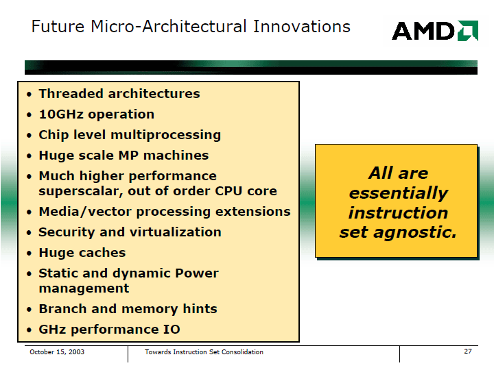
[edit]In 2003, AMD outlined the features for upcoming generations of microprocessors after the K8 family of processors in various events and analyst meetings, including the Microprocessor Forum 2003.[7] The outlined features to be deployed by the next-generation microprocessors are as follows:
- Threaded architectures.
- Chip level multiprocessing.
- Huge scale MP (multi-processor) machines.
- 10 GHz operation.
- Much higher performance superscalar, out-of-order CPU core.
- Huge caches.
- Media/vector processing extensions.
- Branch and memory hints.
- Security and virtualization.
- Enhanced Branch Predictors.
- Static and dynamic power management.
In June 2006, AMD executive vice president Henri Richard had an interview with DigiTimes commented on the upcoming processor developments:
Q: What is your broad perspective on the development of AMD processor technology over the next three to four years?
A: Well, as Dirk Meyer commented at our analysts meeting, we're not standing still. We've talked about the refresh of the current K8 architecture that will come in '07, with significant improvements in many different areas of the processor, including integer performance, floating point performance, memory bandwidth, interconnections and so on.
— AMD Executive Vice President, Henri Richard, Source: DigiTimes Interview with Henri Richard[8]
Live demonstrations
[edit]On November 30, 2006, AMD live demonstrated the native quad core chip known as "Barcelona" for the first time in public,[9] while running Windows Server 2003 64-bit Edition. AMD claims 70% scaling of performance in real world loads, and better performance than Intel Xeon 5355 processor codenamed Clovertown.[10]
On January 24, 2007, AMD Executive Vice President Randy Allen claimed that in live tests, in regard to a wide variety of workloads, "Barcelona" was able to demonstrate 40% performance advantage over the comparable Intel Xeon codenamed Clovertown dual-processor (2P) quad-core processors.[11] The expected performance of floating point per core would be approximately 1.8 times that of the K8 family, at the same clock speed.[12]
On May 10, 2007, AMD held a private event demonstrating the upcoming processors codenamed Agena FX and chipsets, with one demonstrated system being AMD Quad FX platform with one Radeon HD 2900 XT graphics card on the upcoming RD790 chipset. The system was also demonstrated real-time converting a 720p video clip into another undisclosed format while all 8 cores were maxed at 100% by other tasks.[13]
Sister microarchitecture
[edit]On the December 2006 analyst day, Executive vice president Marty Seyer announced a new mobile core codenamed Griffin launched in 2008 with inherited power optimizations technologies from the K10 microarchitecture, but based on a K8 design.
TLB bug
[edit]In November 2007 AMD stopped delivery of Barcelona processors after a bug in the translation lookaside buffer (TLB) of stepping B2 was discovered that could rarely lead to a race condition and thus a system lockup.[14] A patch in BIOS or software worked around the bug by disabling cache for page tables, but it was connected to a 5 to 20% performance penalty. Kernel patches that would almost completely avoid this penalty were published for Linux. In April 2008, the new stepping B3 was brought to the market by AMD, including a fix for the bug plus other minor enhancements.[15]
Features
[edit]Fabrication technology
[edit]AMD has introduced the microprocessors manufactured at 65 nm feature width using Silicon-on-insulator (SOI) technology, since the release of K10 coincides with the volume ramp of this manufacturing process.[16]
Supported DRAM standards
[edit]The K8 family was known to be particularly sensitive to memory latency since its design gains performance by minimizing this through the use of an on-die memory controller (integrated into the CPU); increased latency in the external modules negates the usefulness of the feature. DDR2 RAM introduces some additional latency over DDR RAM since the DRAM is internally driven by a clock at one quarter of the external data frequency, as opposed to one half that of DDR. However, since the command clock rate in DDR2 is doubled relative to DDR and other latency-reducing features (e.g. additive latency) have been introduced, common comparisons based on CAS latency alone are not sufficient. For example, Socket AM2 processors are known to demonstrate similar performance using DDR2 SDRAM as Socket 939 processors that utilize DDR-400 SDRAM. K10 processors support DDR2 SDRAM rated up to DDR2-1066 (1066 MHz).[17]
While some desktop K10 processors are AM2+ supporting only DDR2, an AM3 K10 processor supports both DDR2 and DDR3. A few AM3 motherboards have both DDR2 and DDR3 slots (this does not mean that both types can be fitted at the same time), but for the most part they have only DDR3.
Lynx desktop processors only support DDR3, as they use the FM1 socket.
Microarchitecture characteristics
[edit]

Characteristics of the microarchitecture include the following:[18]
- Form factors
- Socket AM2+ with DDR2 for the 65 nm Phenom and Athlon 7000 Series
- Socket AM3 with either DDR2 or DDR3 for Semprons and the 45 nm Phenom II and Athlon II Series. They can also be used on AM3+ motherboards with DDR3. Note that, while all K10 Phenom Processors are backwards compatible with Socket AM2+ and Socket AM2, some 45 nm Phenom II Processors are only available for Socket AM2+. Lynx processors do not use either AM2+ nor AM3.
- Socket FM1 with DDR3 for Lynx processors.
- Socket F with DDR2, DDR3 with Shanghai and later Opteron processors
- Instruction set additions and extensions
- New bit-manipulation instructions ABM: Leading Zero Count (LZCNT) and Population Count (POPCNT)
- New SSE instructions named as SSE4a: combined mask-shift instructions (EXTRQ/INSERTQ) and scalar streaming store instructions (MOVNTSD/MOVNTSS). These instructions are not found in Intel's SSE4
- Support for unaligned SSE load-operation instructions (which formerly required 16-byte alignment)[19]
- Execution pipeline enhancements
- 128-bit wide SSE units
- Wider L1 data cache interface allowing for two 128-bit loads per cycle (as opposed to two 64-bit loads per cycle with K8)
- Lower integer divide latency
- 512-entry indirect branch predictor and a larger return stack (size doubled from K8) and branch target buffer
- Side-Band Stack Optimizer, dedicated to perform increment/decrement of register stack pointer
- Fastpathed CALL and RET-Imm instructions (formerly microcoded) as well as MOVs from SIMD registers to general purpose registers
- Integration of new technologies onto CPU die:
- Four processor cores (Quad-core)
- Split power planes for CPU core and memory controller/northbridge for more effective power management, first dubbed Dynamic Independent Core Engagement or D. I. C. E. by AMD and now known as Enhanced PowerNow! (also dubbed Independent Dynamic Core Technology), allowing the cores and northbridge (integrated memory controller) to scale power consumption up or down independently.[20]
- Shutting down portions of the circuits in core when not in load, named "CoolCore" Technology.
- Improvements in the memory subsystem:
- Improvements in access latency:
- Support for re-ordering loads ahead of other loads and stores
- More aggressive instruction prefetching, 32 bytes instruction prefetch as opposed to 16 bytes in K8
- DRAM prefetcher for buffering reads
- Buffered burst writeback to RAM in order to reduce contention
- Changes in memory hierarchy:
- Prefetch directly into L1 cache as opposed to L2 cache with K8 family
- 32-way set associative L3 victim cache sized at least 2 MB, shared between processing cores on a single die (each with 512 K of independent exclusive L2 cache), with a sharing-aware replacement policy.
- Extensible L3 cache design, with 6 MB planned for 45 nm process node, with the chips codenamed Shanghai.
- Changes in address space management:
- Two 64-bit independent memory controllers, each with its own physical address space; this provides an opportunity to better utilize the available bandwidth in case of random memory accesses occurring in heavily multi-threaded environments. This approach is in contrast to the previous "interleaved" design, where the two 64-bit data channels were bounded to a single common address space.
- Larger Tagged Lookaside Buffers; support for 1 GB page entries and a new 128-entry 2 MB page TLB
- 48-bit memory addressing to allow for 256 TB memory subsystems[21]
- Memory mirroring (alternatively mapped DIMM addressing),[22] data poisoning support and Enhanced RAS
- AMD-V Nested Paging for improved MMU virtualization, claimed to have decreasing world switch time by 25%.
- Improvements in access latency:
- Improvements in system interconnect:
- HyperTransport retry support
- Support for HyperTransport 3.0, with HyperTransport Link unganging which creates 8 point-to-point links per socket.
- Platform-level enhancements with additional functionality:
- Five p-states allowing for automatic clock rate modulation
- Increased clock gating
- Official support for coprocessors via HTX slots and vacant CPU sockets through HyperTransport: Torrenza initiative.
Feature tables
[edit]Desktop
[edit]Phenom models
[edit]Agena (65 nm SOI, quad-core)
[edit]- Four AMD K10 cores
- L1 cache: 64 KB instruction and 64 KB data[23] (data + instructions) per core
- L2 cache: 512 KB per core, full-speed
- L3 cache: 2 MB shared between all cores
- Memory controller: dual channel DDR2-1066 MHz with unganging option
- ISA extensions: MMX, Enhanced 3DNow!, SSE, SSE2, SSE3, SSE4a, ABM, AMD64, Cool'n'Quiet, NX bit, AMD-V
- Socket AM2+, HyperTransport with 1600 to 2000 MHz
- Power consumption (TDP): 65, 95, 125 and 140 Watt
- First release
- November 19, 2007 (B2 Stepping)
- March 27, 2008 (B3 Stepping)
- Clock rate: 1800 to 2600 MHz
- Models: Phenom X4 9100e - 9950
Toliman (65 nm SOI, tri-core)
[edit]- Three AMD K10 cores
- L1 cache: 64 KB instruction and 64 KB data cache per core
- L2 cache: 512 KB per core, full-speed
- L3 cache: 2 MB shared between all cores
- Memory controller: dual channel DDR2-1066 MHz with unganging option
- ISA extensions: MMX, Enhanced 3DNow!, SSE, SSE2, SSE3, SSE4a, ABM, AMD64, Cool'n'Quiet, NX bit, AMD-V
- Socket AM2+, HyperTransport with 1600 to 1800 MHz
- Power consumption (TDP): 65 and 95 Watt
- First release
- March 27, 2008 (B2 Stepping)
- April 23, 2008 (B3 Stepping)
- Clock rate: 2100 to 2500 MHz
- Models: Phenom X3 8250e - 8850
Phenom II models
[edit]Thuban (45 nm SOI, hexa-core)
[edit]- Six AMD K10 cores
- L1 cache: 64 KB instructions and 64 KB data per core
- L2 cache: 512 KB per core, full-speed
- L3 cache: 6 MB shared between all cores.
- Memory controller: dual channel DDR2-1066 MHz (AM2+), dual channel DDR3-1333 (AM3) with unganging option
- ISA extensions: MMX, Enhanced 3DNow!, SSE, SSE2, SSE3, SSE4a, ABM, AMD64, Cool'n'Quiet, NX bit, AMD-V
- Socket AM2+, Socket AM3, HyperTransport with 1800 to 2000 MHz
- Power consumption (TDP): 95 or 125 Watt
- First release
- 27 April 2010 (E0 Stepping)
- Clock rate: 2.6 - 3.3 GHz; up to 3.7 GHz with Turbo Core
- Models: Phenom II X6 1035T, 1045T, 1055T, 1065T, 1075T, 1090T and 1100T
Zosma (45 nm SOI, quad-core)
[edit]- Four AMD K10 cores harvested from Thuban with two cores disabled[24]
- ISA extensions: MMX, Enhanced 3DNow!, SSE, SSE2, SSE3, SSE4a, ABM, NX bit, AMD64, Cool'n'Quiet, AMD-V, Turbo Core (AMD equivalent of Intel Turbo Boost)
- Memory support: DDR2 SDRAM up to PC2-8500, DDR3 SDRAM up to PC3-10600 (Socket AM3 only)
- Models: Phenom II X4 650T, 840T, 960T, 970 (Thuban-based Zosma core, OEM Only, 970 has unlocked multiplier but w/o Turbo Core)
Deneb (45 nm SOI, quad-core)
[edit]- Four AMD K10 cores
- L1 cache: 64 KB instructions and 64 KB data per core
- L2 cache: 512 KB per core, full-speed
- L3 cache: 6 MB shared between all cores. The 800 series have 2 MB of its L3 Cache disabled due to defects.
- Memory controller: dual channel DDR2-1066 MHz (AM2+), dual channel DDR3-1333 (AM3) with unganging option
- ISA extensions: MMX, Enhanced 3DNow!, SSE, SSE2, SSE3, SSE4a, ABM, AMD64, Cool'n'Quiet, NX bit, AMD-V
- Socket AM2+, Socket AM3, HyperTransport with 1800 to 2000 MHz
- Power consumption (TDP): 65, 95, 125 and 140 Watt
- First release
- 8 January 2009 (C2 Stepping)
- Clock rate: 2500 to 3700 MHz
- Models: Phenom II X4 805 - 980 (except 840 and 850)
42 TWKR Limited Edition (45 nm SOI, quad-core)
[edit]AMD released a limited edition Deneb-based processor to extreme overclockers and partners. Fewer than 100 were manufactured.
The "42" officially represents four cores running at 2 GHz, but is also a reference to the answer to life, the universe, and everything from The Hitchhiker's Guide to the Galaxy.[25]
- Four AMD K10 cores
- Models: Phenom II 42 TWKR
Propus (45 nm SOI, quad-core)
[edit]- Four AMD K10 cores harvested from Deneb with L3 cache disabled[24]
- ISA extensions: MMX, Enhanced 3DNow!, SSE, SSE2, SSE3, SSE4a, ABM, NX bit, AMD64, Cool'n'Quiet, AMD-V
- Memory support: DDR2 SDRAM up to PC2-8500 (DDR2-1066 MHz), DDR3 SDRAM up to PC3-10600 (DDR3-1333 MHz) (Socket AM3 only)
- Models: Phenom II X4 840 and 850
Heka (45 nm SOI, tri-core)
[edit]- Three AMD K10 cores using chip harvesting technique, with one core disabled
- L1 cache: 64 KB instructions and 64 KB data per core
- L2 cache: 512 KB per core, full-speed
- L3 cache: 6 MB shared between all cores
- Memory controller: dual channel DDR2-1066 MHz (AM2+), dual channel DDR3-1333 (AM3) with unganging option
- ISA extensions: MMX, Enhanced 3DNow!, SSE, SSE2, SSE3, SSE4a, ABM, AMD64, Cool'n'Quiet, NX bit, AMD-V
- Socket AM3, HyperTransport with 2000 MHz
- Power consumption (TDP): 65 and 95 Watt
- First release
- 9 February 2009 (C2 Stepping)
- Clock rate: 2500 to 3000 MHz
- Models: Phenom II X3 705e - 740
Callisto (45 nm SOI, dual-core)
[edit]- Two AMD K10 cores using chip harvesting technique, with two cores disabled
- L1 cache: 64 KB instructions and 64 KB data per core
- L2 cache: 512 KB per core, full-speed
- L3 cache: 6 MB shared between all cores
- Memory controller: dual channel DDR2-1066 MHz (AM2+), dual channel DDR3-1333 (AM3) with unganging option
- ISA extensions: MMX, Enhanced 3DNow!, SSE, SSE2, SSE3, SSE4a, ABM, AMD64, Cool'n'Quiet, NX bit, AMD-V
- Socket AM3, HyperTransport with 2000 MHz
- Power consumption (TDP): 80 Watt
- First release
- 1 June 2009 (C2 Stepping)
- Clock rate: 3000 to 3500 MHz
- Models: Phenom II X2 545 - 570
Regor (45 nm SOI, dual-core)
[edit]- Two AMD K10 cores
- Some are chip harvests from Propus or Deneb with two cores disabled[24]
- Most Regor-based processors feature double the L2 cache per core (1 MB) as other Athlon II and Phenom II processors.
- ISA extensions: MMX, Enhanced 3DNow!, SSE, SSE2, SSE3, SSE4a, ABM, NX bit, AMD64, Cool'n'Quiet, AMD-V
- Memory support: DDR2 SDRAM up to PC2-8500, DDR3 SDRAM up to PC3-8500 (DDR3-1066 MHz) (Socket AM3 only)
- Models: Phenom II X2 511 and 521
Athlon X2 models
[edit]Kuma (65 nm SOI, dual-core)
[edit]- Two AMD K10 cores harvested from Agena with two cores disabled[24]
- ISA extensions: MMX, Enhanced 3DNow!, SSE, SSE2, SSE3, SSE4a, ABM, NX bit, AMD64, Cool'n'Quiet, AMD-V[26]
- Models: Athlon X2 6500 - 7850
Regor/Deneb (45 nm SOI, dual-core)
[edit]- Two AMD K10 cores. Some 5000 series processors are chip harvests from Propus or Deneb; All 5200 series chips are harvests, each has two cores disabled[24]
- ISA extensions: MMX, Enhanced 3DNow!, SSE, SSE2, SSE3, SSE4a, ABM, NX bit, AMD64, Cool'n'Quiet, AMD-V[26]
- Models: Athlon X2 5000+ and 5200+
Athlon II Models
[edit]Zosma (45 nm SOI, quad-core)
[edit]- Four AMD K10 cores harvested from Thuban with two cores disabled[24]
- ISA extensions: MMX, Enhanced 3DNow!, SSE, SSE2, SSE3, SSE4a, ABM, NX bit, AMD64, Cool'n'Quiet, AMD-V, Turbo Core (AMD equivalent of Intel Turbo Boost)
- Memory support: DDR2 SDRAM up to PC2-8500, DDR3 SDRAM up to PC3-10600 (Socket AM3 only)
- Models: Athlon II X4 640[T]
Propus (45 nm SOI, quad-core)
[edit]- Four AMD K10 cores[27][28]
- L1 cache: 64 KB instructions and 64 KB data per core
- L2 cache: 512 KB per core, full-speed
- Memory controller: dual channel DDR2-1066 MHz (AM2+), dual channel DDR3-1333 (AM3) with unganging option
- ISA extensions: MMX, Enhanced 3DNow!, SSE, SSE2, SSE3, SSE4a, ABM, AMD64, Cool'n'Quiet, NX bit, AMD-V
- Socket AM3, HyperTransport with 2000 MHz
- Power consumption (TDP): 45 Watt or 95 Watt
- First release
- September 2009 (C2 Stepping)
- Clock rate: 2200 - 3100 MHz
- Models: Athlon II X4 600e - 650
Rana (45 nm SOI, tri-core)
[edit]- Three AMD K10 cores chip harvested from Propus or Deneb with one core disabled[24]
- L1 cache: 64 kB + 64 kB (data + instructions) per core
- L2 cache: 512 kB per core, full-speed
- Memory controller: dual channel DDR2-1066 MHz (AM2+), dual channel DDR3-1333 (AM3) with unganging option
- ISA extensions: MMX, Enhanced 3DNow!, SSE, SSE2, SSE3, SSE4a, ABM, AMD64, Cool'n'Quiet, NX bit, AMD-V
- Socket AM3, HyperTransport with 2 GHz
- Die Size: 169 mm2[29]
- Power consumption (TDP): 45 Watts or 95 Watts
- First release
- October 2009 (Stepping C2)
- Clock rate: 2.2–3.4 GHz
- Models: Athlon II X3 400e - 460
Regor (45 nm SOI, dual-core)
[edit]- Two AMD K10 cores
- L1 cache: 64 KB instructions and 64 KB data per core
- L2 cache: 1024 KB per core, full-speed
- Memory controller: dual channel DDR2-1066 MHz (AM2+), dual channel DDR3-1333 (AM3) with unganging option
- ISA extensions: MMX, Enhanced 3DNow!, SSE, SSE2, SSE3, SSE4a, ABM, AMD64, Cool'n'Quiet, NX bit, AMD-V
- Socket AM3, HyperTransport with 2000 MHz
- Power consumption (TDP): 65 Watt
- First release
- June 2009 (C2 Stepping)
- Clock rate: 1600 - 3600 MHz
- Models: Athlon II X2 250u - 280
Sargas (45 nm SOI, single-core)
[edit]- Single AMD K10 core harvest from Regor with one core disabled[24]
- ISA extensions: MMX, Enhanced 3DNow!, SSE, SSE2, SSE3, SSE4a, ABM, NX bit, AMD64, Cool'n'Quiet, AMD-V
- Memory support: DDR2 SDRAM up to PC2-6400, DDR3 SDRAM up to PC3-8500 (Socket AM3 only)
- Models: Athlon II 160u and 170u
Lynx (32 nm SOI, dual or quad-core)
[edit]- Two or four AMD K10 cores with no L3 cache
- APUs without graphics. See below.
- Models: Athlon II X2 221 to Athlon II X4 651K
Sempron models
[edit]Sargas (45 nm SOI, single-core)
[edit]- Single AMD K10 core chip harvested from Regor with one core disabled[24]
- ISA extensions: MMX, Enhanced 3DNow!, SSE, SSE2, SSE3, SSE4a, ABM, NX bit, AMD64, Cool'n'Quiet, AMD-V
- Models: Sempron 130-150
Sempron X2 models
[edit]Regor (45 nm SOI, dual-core)
[edit]- Two AMD K10 cores
- ISA extensions: MMX, Enhanced 3DNow!, SSE, SSE2, SSE3, SSE4a, ABM, NX bit, AMD64, Cool'n'Quiet, AMD-V
- Models: Sempron X2 180 and 190
Lynx (32 nm SOI, dual-core)
[edit]- Two AMD K10 cores with no L3 cache
- APUs without graphics. See below.
- Models: Sempron X2 198
Llano "APUs"
[edit]Lynx (32 nm SOI, dual or quad-core)
[edit]The first generation desktop APUs based on the K10 microarchitecture were released in 2011 (some models do not provide graphics capability, such as the Lynx Athlon II and Sempron X2).
- Fabrication 32 nm on GlobalFoundries SOI process
- Socket FM1
- Die size: 228 mm2, with 1.178 billion transistors[30][31]
- AMD K10 cores with no L3 cache
- GPU: TeraScale 2
- All A and E series models feature Redwood-class integrated graphics on die (BeaverCreek for the dual-core variants and WinterPark for the quad-core variants). Sempron and Athlon models exclude integrated graphics.[32]
- Support for up to four DIMMs of up to DDR3-1866 memory
- 5 GT/s UMI
- Integrated PCIe 2.0 controller
- Select models support Turbo Core technology for faster CPU operation when the thermal specification permits
- Select models support Hybrid Graphics technology to assist a discrete Radeon HD 6450, 6570, or 6670 discrete graphics card. This is similar to the current Hybrid CrossFireX technology available in the AMD 700 and 800 chipset series
- ISA extensions: MMX, Enhanced 3DNow!, SSE, SSE2, SSE3, SSE4a, ABM, NX bit, AMD64, Cool'n'Quiet, AMD-V
- Models: Lynx desktop APUs and CPUs
Mobile
[edit]Turion II (Ultra) models
[edit]"Caspian" (45nm SOI, dual-core)
[edit]- Tigris platform[33]
- Two AMD K10 cores
- ISA extensions: MMX, Enhanced 3DNow!, SSE, SSE2, SSE3, SSE4a, ABM, NX bit, AMD64, AMD-V, PowerNow!
- Memory support: DDR2 SDRAM (Up to 800 MHz)
- Models: Turion II Ultra M600 to M660
Turion II models
[edit]"Caspian" (45nm SOI, dual-core)
[edit]- Tigris platform
- Two AMD K10 cores
- ISA extensions: MMX, Enhanced 3DNow!, SSE, SSE2, SSE3, SSE4a, ABM, NX bit, AMD64, AMD-V, PowerNow!
- Memory support: DDR2 SDRAM (Up to 800 MHz)
- Models: Turion II M500 TO M560
"Champlain" (45nm SOI, dual-core)
[edit]- Danube platform[34][35]
- Two AMD K10 cores
- ISA extensions: MMX, Enhanced 3DNow!, SSE, SSE2, SSE3, SSE4a, ABM, NX bit, AMD64, AMD-V, PowerNow!
- Memory support: DDR3 SDRAM, DDR3L SDRAM (Up to 1333 MHz)
- Models: Turion II models
Athlon II models
[edit]"Caspian" (45nm SOI, dual-core)
[edit]- Tigris platform
- Two AMD K10 cores
- ISA extensions: MMX, Enhanced 3DNow!, SSE, SSE2, SSE3, SSE4a, ABM, NX bit, AMD64, AMD-V, PowerNow!
- Memory support: DDR2 SDRAM (Up to 800 MHz)
- Models: Athlon II M300 to M360
"Champlain" (45nm SOI, dual-core)
[edit]- Danube platform
- Two AMD K10 cores
- ISA extensions: MMX, Enhanced 3DNow!, SSE, SSE2, SSE3, SSE4a, ABM, NX bit, AMD64, AMD-V, PowerNow!
- Memory support: DDR3 SDRAM, DDR3L SDRAM (Up to 1333 MHz)
- Models: Athlon II models
Sempron models
[edit]"Caspian" (45nm SOI, single-core)
[edit]- Tigris platform
- Single AMD K10 core
- ISA extensions: MMX, Enhanced 3DNow!, SSE, SSE2, SSE3, SSE4a, ABM, NX bit, AMD64, AMD-V, PowerNow!
- Memory support: DDR2 SDRAM (Up to 800 MHz)
- Models: Sempron M100 to M140
Turion II Neo models
[edit]"Geneva" (45nm SOI, dual-core)
[edit]- Nile platform[34][36]
- Two AMD K10 cores
- ISA extensions: MMX, Enhanced 3DNow!, SSE, SSE2, SSE3, SSE4a, ABM, NX bit, AMD64, AMD-V, PowerNow!
- Memory support: DDR3 SDRAM, DDR3L SDRAM (Up to 1066 MHz)
- Models: Turion II Neo models
Athlon II Neo models
[edit]"Geneva" (45nm SOI, dual-core)
[edit]- Nile platform
- Two AMD K10 cores
- ISA extensions: MMX, Enhanced 3DNow!, SSE, SSE2, SSE3, SSE4a, ABM, NX bit, AMD64, AMD-V, PowerNow!
- Memory support: DDR3 SDRAM, DDR3L SDRAM (Up to 1066 MHz)
- Models: Athlon II Neo models
"Geneva" (45nm SOI, single-core)
[edit]- Nile platform
- Single AMD K10 core
- ISA extensions: MMX, Enhanced 3DNow!, SSE, SSE2, SSE3, SSE4a, ABM, NX bit, AMD64, AMD-V, PowerNow!
- Memory support: DDR3 SDRAM, DDR3L SDRAM (Up to 1066 MHz)
- Models: Athlon II K125 and K145
V models
[edit]"Geneva" (45nm SOI, single-core)
[edit]- Nile platform
- Single AMD K10 core
- ISA extensions: MMX, Enhanced 3DNow!, SSE, SSE2, SSE3, SSE4a, ABM, NX bit, AMD64, AMD-V, PowerNow!
- Memory support: DDR3 SDRAM, DDR3L SDRAM (Up to 1066 MHz)
- Models: V 105
"Champlain" (45nm SOI, single-core)
[edit]- Danube platform
- Single AMD K10 core
- ISA extensions: MMX, Enhanced 3DNow!, SSE, SSE2, SSE3, SSE4a, ABM, NX bit, AMD64, AMD-V, PowerNow!
- Memory support: DDR3 SDRAM, DDR3L SDRAM (Up to 1333 MHz)
- Models: V 120 to 160
Phenom II models
[edit]"Champlain" (45nm SOI, quad-core)
[edit]- Danube platform
- Four AMD K10 cores
- Unlike desktop models, mobile Phenom II models do not have L3 cache
- ISA extensions: MMX, Enhanced 3DNow!, SSE, SSE2, SSE3, SSE4a, ABM, NX bit, AMD64, AMD-V, PowerNow!
- Memory support: DDR3 SDRAM, DDR3L SDRAM (Up to 1333 MHz)
- Models: Phenom II models
"Champlain" (45nm SOI, tri-core)
[edit]- Danube platform
- Three AMD K10 cores
- Unlike desktop models, mobile Phenom II models do not have L3 cache
- ISA extensions: MMX, Enhanced 3DNow!, SSE, SSE2, SSE3, SSE4a, ABM, NX bit, AMD64, AMD-V, PowerNow!
- Memory support: DDR3 SDRAM, DDR3L SDRAM (Up to 1333 MHz)
- Models: Phenom II models
"Champlain" (45nm SOI, dual-core)
[edit]- Danube platform
- Two AMD K10 cores
- Unlike desktop models, mobile Phenom II models do not have L3 cache
- ISA extensions: MMX, Enhanced 3DNow!, SSE, SSE2, SSE3, SSE4a, ABM, NX bit, AMD64, AMD-V, PowerNow!
- Memory support: DDR3 SDRAM, DDR3L SDRAM (Up to 1333 MHz)
- Models: Phenom II models
Llano APUs
[edit]"Sabine" (32nm SOI, dual or quad-core)
[edit]- Fabrication 32 nm on GlobalFoundries' SOI process
- Socket FS1
- Two or four upgraded K10 cores codenamed Husky[citation needed] (K10.5[citation needed]) with no L3 cache, and with Redwood-class integrated graphics on die (WinterPark for the dual-core variants and BeaverCreek for the quad-core variants)
- Integrated PCIe 2.0 controller
- GPU: TeraScale 2
- Select models support Turbo Core technology for faster CPU operation when the thermal specification permits
- 2.5 GT/s UMI
- ISA extensions: MMX, Enhanced 3DNow!, SSE, SSE2, SSE3, SSE4a, ABM, NX bit, AMD64, AMD-V, PowerNow!
- Support for 1.35 V DDR3L-1333 memory, in addition to regular 1.5 V DDR3 memory specified
- Models: Sabine mobile APUs
Server
[edit]Successor
[edit]AMD discontinued further development of K10 based CPUs after Thuban, choosing to focus on Fusion products for mainstream desktops and laptops and Bulldozer based products for the performance market. However, within the Fusion product family, APUs such as the first generation A4, A6 and A8-series chips (Llano APUs) continued to use K10-derived CPU cores in conjunction with a Radeon graphics core. K10 and its derivatives were phased out of production by the introduction of Trinity-based APUs in 2012, which replaced the K10 cores in the APU with Bulldozer-derived cores.
Family 11h and 12h derivatives
[edit]Turion X2 Ultra Family 11h
[edit]The Family 11h microarchitecture was a mixture of both K8 and K10 designs with lower power consumption for laptop that was marketed as Turion X2 Ultra and was later replaced by completely K10-based designs.[1]
Fusion Family 12h
[edit]The Family 12h microarchitecture is a derivative of the K10 design:[37][38]
- Both CPU and GPU were re-used to avoid complexity and risk
- Distinct Software and Physical integration makes Fusion (APU) microarchitectures different
- Power-saving improvements including clock gating
- Improvements to hardware pre-fetcher
- Redesigned memory controller
- 1MB L2 cache per core
- No L3 cache
- Two new buses for on-die GPU to access memory (called Onion and Garlic interfaces)
- AMD Fusion Compute Link (Onion) – interfaces to CPU cache and coherent system memory (see cache coherence)
- Radeon Memory Bus (Garlic) – dedicated non-coherent interface connected directly to memory
Media discussions
[edit]Note: These media discussions are listed in ascending date of publication.
- "AMD CTO speaks about future AMD technologies". AnandTech. 2005-10-14. Archived from the original on November 4, 2005.
- "AMD outlines Future Goals (mostly non-specific at this time)". TechReport. 2005-10-17. Archived from the original on 2006-12-30. Retrieved 2006-08-19.
- "AMD eyes Z-RAM for dense caches". CNet News. 2006-01-20.
- "AMD licenses Z-RAM". SlashDot. 2006-01-21.
- "AMD's K8L to double FPU units in 2007". Geek.com. 2006-02-24. Archived from the original on 2016-01-12. Retrieved 2015-06-07.
- "Rev G. and H. AMD64 chips Preliminary information". The Inquirer. 2006-03-03. Archived from the original on March 12, 2006.
- "Interview with Henri Richard (Part 2)". DigiTimes. 2006-03-14.
- "AMD demonstrates Hardware Coprocessor Offload". LinuxElectrons. 2006-03-20. Archived from the original on 2006-10-21.
- "Implementation of FPGA through coherent HTT". The Inquirer. 2006-03-26. Archived from the original on January 12, 2016.
- "AMD's K8L 65 nm core due H1 07". Reg Hardware. 2006-04-04. Archived from the original on 2007-05-24. Retrieved 2007-04-19.
- "An AMD Update: Fab 36 Begins Shipments, Planning for 65 nm and AM2 Performance". AnandTech. 2006-04-04. Archived from the original on April 6, 2006.
- "Fab36 substantially converted to 65 nm by mid-2007". AnandTech. 2006-04-04. Archived from the original on April 6, 2006.
- "AMD shows off details of K8L". The Inquirer. 2006-05-16. Archived from the original on June 14, 2006.
- "AMD's K8L and 4x4 Preview". RealWorldtech. 2006-06-02.
- "AMD K8L and 4X4 Technologies". ArsTechnica. 2006-06-02.
- "AMD Quad-Core K8L & 4x4 Details". Pure OverClock. 2006-06-03. Archived from the original on February 9, 2012.
- "Socket AM2 Forward Compatible With AM3 CPUs". DailyTech. 2006-07-06. Archived from the original on 2007-06-08.
- "K8L on schedule, due for release as early as Q1 07". The Inquirer. 2006-07-11. Archived from the original on September 6, 2007.
- "GNU binutils support for the new K10 instructions". SourceWare.org. 2006-07-13.
- "AMD Executives Confirm K8L to Arrive in Mid-2007". X-bit labs. 2006-07-21. Archived from the original on 2006-11-26.
- "AMD To Demo K8L By Year End". moneycontrol.com. 2006-07-23. Archived from the original on August 18, 2007.
- "AMD intros new Opterons and promises 68 W quad-core CPUs". tgdaily.com. 2006-08-15. Archived from the original on 2006-08-21.
- "Next-Generation AMD Opteron Paves The Way For Quad-Core". crn.com. 2006-08-15. Archived from the original on 2012-02-06. Retrieved 2007-04-19.
- "AMD's Next Generation Microarchitecture Preview: from K8 to K8L". X-bit labs. 2006-08-21. Archived from the original on 2006-08-27.
- "AMD quad cores: the whole story unfolded". The Inquirer. 2006-09-16. Archived from the original on May 19, 2007.
- "AMD reinvents the x86". InfoWorld. 2007-02-07. Archived from the original on December 7, 2008.
- "Inside Barcelona: AMD's Next Generation". RealWorldTech. 2007-05-16.
See also
[edit]References
[edit]- ^ a b "List of AMD CPU microarchitectures - LeonStudio". LeonStudio - CodeFun. 3 August 2014. Archived from the original on 26 September 2020. Retrieved 12 September 2015.
- ^ Hesseldahl, Arik (2000-07-06). "Why Cool Chip Code Names Die". forbes.com. Retrieved 2007-07-14.
- ^ "The Inquirer report". The Inquirer. Archived from the original on September 6, 2007.
- ^ a b Valich, Theo. "AMD explains K8L misnomer". The Inquirer. Archived from the original on February 10, 2007. Retrieved 2007-03-16.
- ^ Official Announcement of "AMD Next Generation Processor Technology"
- ^ Video interview of Giuseppe Amato (AMD's Technical Director, Sales and Marketing EMEA) Archived 2009-07-12 at archive.today in February 2007
- ^ Microprocessor Forum 2003 presentation slide
- ^ AMD's vision for next few years - an interview with Henri Richard
- ^ "AMD Demonstrates Its Quad Core Server Chips". CNET.com. 2006-11-30.
- ^ "AMD Demonstrates Barcelona; The First True, Native Quad Core Opteron". legitreviews.com. 2006-11-30.
- ^ "AMD Expects Quad Core Barcelona to Outperform Clovertown by 40%". dailytech.com. 2007-01-25. Archived from the original on 2007-02-27. Retrieved 2007-04-19.
- ^ "Go to 'Barcelona' over 'Cloverton'". CNET.com. 2007-01-23.
- ^ "TGDaily report". Archived from the original on 2007-09-26. Retrieved 2007-05-11.
- ^ "Understanding AMD's TLB Processor Bug". Daily Tech. Archived 2009-02-18 at the Wayback Machine. December 5, 2007
- ^ "TLB Bug – in the Past". Xbit Labs. Archived 2009-02-09 at the Wayback Machine. March 26, 2008
- ^ "An AMD Update: Fab 36 Begins Shipments, Planning for 65 nm process and AM2 Performance". AnandTech. 2006-04-04. Archived from the original on April 6, 2006.
- ^ "AMD's next-generation Star supports DDR2-1066 & SSE4a". HKEPC Hardware. Retrieved 2007-03-19.
- ^ Shimpi, Anand Lal. "Barcelona Architecture: AMD on the Counterattack". AnandTech. Archived from the original on 19 March 2007. Retrieved 2007-03-18.
- ^ Case, Loyd. "AMD Unveils Barcelona Quad-Core Details". Ziff Davis. Retrieved 2007-03-18.[dead link]
- ^ "AMD Next Generation Processor Technology Slides". HardOCP. 2006-08-22.
- ^ "BIOS and Kernel Developer's Guide (BKDG) For AMD Family 10h Processors" (PDF). p. 24. Archived from the original (PDF) on June 9, 2011. Retrieved 2010-05-29.
Physical address space increased to 48 bits.
- ^ "BIOS and Kernel Developer's Guide (BKDG) for AMD Family 15h Models 10h-1Fh Processors" (PDF). support.amd.com. Advanced Micro Devices. June 4, 2013. p. 340. Retrieved January 25, 2015.
- ^ In this article, the conventional prefixes for computer memory denote base-2 values whereby "kilobyte" (KB) = 210 bytes.
- ^ a b c d e f g h i "List of Unlockable AMD CPUs".
- ^ "Legit Reviews - Technology News & Reviews". 27 June 2022.
- ^ a b "AMD Athlon II Key Architectural Features". Advanced Micro Devices. Archived from the original on December 2, 2010. Retrieved July 8, 2010.
- ^ Athlon II: Viele neue Exemplare der neuen Einsteiger-Prozessoren von AMD
- ^ In arrivo nuovi processori Athlon II da AMD Archived July 10, 2011, at the Wayback Machine
- ^ "AMD Phenom II X6: Thuban the Dragon". Archived from the original on 2014-07-16. Retrieved 2018-03-29.
- ^ Theo Valich (28 May 2012). "AMD Comes Clean on Transistor Numbers With FX, Fusion Processors". Retrieved 23 August 2013.
- ^ Anand Lal Shimpi (27 September 2012). "AMD A10-5800K & A8-5600K Review: Trinity on the Desktop, Part 1". Archived from the original on September 29, 2012. Retrieved 23 August 2013.
- ^ "AMD launches A-Series and the first 32nm Athlon II X4 CPUs". Retrieved 2013-11-10.
- ^ "The 2009 AMD Mainstream Platform". Amd.com. Archived from the original on 2012-05-27. Retrieved 2014-04-30.
- ^ a b "AMD M880G Chipset". Amd.com. Retrieved 2014-04-30.
- ^ "The 2010 AMD Mainstream Platform". Amd.com. Retrieved 2014-04-30.
- ^ "The 2010 AMD Ultrathin Platform". Amd.com. Archived from the original on 2012-10-31. Retrieved 2014-04-30.
- ^ David Kanter (27 June 2011). "AMD Fusion Architecture and Llano". Real World Tech. Retrieved 12 September 2015.
- ^ Pierre Boudier; Graham Sellers (June 2011). "Memory System on Fusion APUs - The Benefits of Zero Copy" (PDF). AMD Fusion Developer Summit.
External links
[edit]- AMD Official Website
- AMD Quad-core processors introduction
- DarkVision Hardware: AMD talks about K9, K10 future innovations
- Next-Generation AMD Opteron Processors Introduced with Record OEM Design Wins and Native Quad-Core Upgrade Path (Official AMD press release on 15 August 2006)
- PC Watch report about K10 based on AMD Technology Analyst Day 2004 and 2005 (in Japanese)
- PC Watch report about K10 based on Slides presented in Microprocessor Forum 2003 (in Japanese)
- "Slides of AMD 2006 Technology Analyst Day: Official Introduction of K10 Microarchitecture" (PDF). Archived from the original on 2009-03-26.
{{cite web}}: CS1 maint: bot: original URL status unknown (link) (2.17 MB) - Software Optimization Guide for AMD Family 10h and 12h Processors
- TechReport: AMD outlines Future Goals
- TweakTown Discussions (2003)
- X-bit labs: AMD K10 Micro-Architecture
AMD 10h
View on GrokipediaOverview and Nomenclature
Introduction
The AMD Family 10h, also known as the K10 microarchitecture, is a 64-bit x86 processor architecture developed by Advanced Micro Devices (AMD) as the successor to the K8 (Family 0Fh) microarchitecture. Introduced in 2007 with the launch of the quad-core Opteron "Barcelona" server processors, K10 marked AMD's shift toward native multi-core designs on a single die, building on the integrated memory controller and HyperTransport interconnect first pioneered in K8. This architecture powered both server and desktop processors, including the Phenom family, emphasizing scalability for high-performance computing workloads.[4] The primary goals of the K10 microarchitecture were to deliver substantial improvements in integer and floating-point performance—up to 50% over prior generations—while enhancing power efficiency through innovations like AMD CoolCore Technology and Dual Dynamic Power Management.[5] These advancements enabled better handling of multi-threaded applications in data centers and consumer systems, with support for configurations scaling to 6 cores in desktop processors and up to 12 cores in server variants using multi-chip modules.[4] By integrating these features, K10 aimed to reduce latency and power consumption compared to discrete-component designs prevalent at the time.[6] Key specifications of K10 include an on-die integrated memory controller supporting DDR2 (and DDR3 in later implementations) memory for lower latency access, and the HyperTransport 2.0 interconnect (up to 2.0 GT/s), with later revisions supporting HyperTransport 3.0 (up to 5.2 GT/s) for inter-processor communication.[5] In historical context, K10 was AMD's strategic response to Intel's Core 2 architecture, which had gained market traction in 2006; AMD positioned K10 to regain competitiveness in both performance benchmarks and energy-efficient multi-core processing for servers and desktops.[6]Naming Conventions
The AMD Family 10h processors were branded across consumer and server segments using established product lines to denote performance tiers and form factors. High-end desktop processors were marketed under the Phenom brand, mid-range desktop models under Athlon II, entry-level desktop variants under Sempron, mobile processors under Turion II, and server-oriented chips under Opteron. These brands were officially trademarked by AMD to distinguish their K10-based offerings from prior generations.[2] Model numbering within these brands followed a consistent scheme emphasizing core count, generation, and features. Suffixes such as "X4" indicated quad-core configurations, while "X2", "X3", and "X6" denoted dual-core, triple-core, and hexa-core models, respectively; for example, the Phenom II X4 targeted mainstream quad-core desktop use. The "II" suffix marked second-generation implementations on the 45 nm process, as seen in Phenom II, Athlon II, and Turion II lines. Unlocked multiplier variants, allowing overclocking, were designated as Black Edition (often abbreviated "BE") or with a star rating symbol (*), such as the Phenom II X4 965 Black Edition. Family 10h revisions, or steppings, were identified via CPUID values and addressed specific hardware errata through silicon updates. Early steppings included B2 (CPUID 00100F22h) and B3 (00100F23h), which were affected by errata such as #254 (TLB livelock, mitigated via MSRC001_1023[7]=1b) and #309 (concurrent L2/NB response issues, mitigated via MSRC001_1023[8]=1b), as well as #263 (DQS distortion, mitigated via BIOS). Later C2 steppings (e.g., RB-C2 at 00100F42h, BL-C2 at 00100F52h) fixed #254 and #309 but not #263. These revisions applied across Opteron, Phenom, Athlon II, and Sempron processors, with errata details documented for developers to ensure compatibility.[2] Internally, AMD used astronomical codenames for Family 10h designs, mapping them to public brands based on target markets. Barcelona served as the codename for the initial quad-core server processor, released as the third-generation Opteron (e.g., 23xx series). Agena was the desktop counterpart, branded as the original Phenom quad-core. Deneb, a 45 nm shrink of Agena, underpinned Phenom II and Athlon II desktop models. Shanghai, another 45 nm evolution, powered updated Opteron processors with enhanced cache, while mobile implementations like Champlain fell under Turion II. These codenames facilitated development tracking before public branding.[9][10]Development and Release
Timeline
The AMD 10h family, also known as K10, was first publicly detailed at AMD's Analyst Day event on December 14, 2006, where the company revealed its roadmap for quad-core processors targeting server, desktop, and mobile segments, with initial shipments planned for late 2007. Originally targeted for a mid-2006 tape-out and broader availability by year-end, development faced significant delays into 2007 primarily due to design bugs encountered during validation and fabrication ramp-up on the 65 nm process node.[11][12] The family's production debut came with the server-oriented Opteron processors codenamed Barcelona, launched on September 10, 2007, as AMD's first native quad-core x86 offerings for data centers, built on 65 nm silicon.[13] Desktop variants followed closely with the Phenom processors introduced on November 19, 2007, also at 65 nm, though early B2-stepping units suffered from a critical translation lookaside buffer (TLB) erratum that could cause system lock-ups under specific memory access patterns, impacting initial shipments and higher clock-speed bins.[14][15] This defect prompted a temporary BIOS workaround that reduced performance by up to 10% in affected workloads, while delaying models like the 2.4 GHz Phenom until revisions could be implemented.[16] AMD addressed the TLB issue hardware-side with the B3 stepping revision, which began shipping on March 27, 2008, enabling higher-volume production and clock speeds without the prior penalties for both Phenom and Barcelona lines.[17] The architecture transitioned to the 45 nm process node later that year, starting with the Opteron "Shanghai" processors launched on November 13, 2008, featuring a shrink to the 45 nm process and larger shared L3 cache for improved efficiency.[18] Desktop evolution continued with the Phenom II series, released in December 2008 on 45 nm, featuring refined cores for better power efficiency and compatibility with DDR2 and DDR3 memory.[19]Launch Demonstrations
The AMD K10 microarchitecture, codenamed 10h, made its initial public appearance with the server-oriented Barcelona Opteron processors. On September 10, 2007, AMD unveiled the Quad-Core AMD Opteron at a premiere event in San Francisco, demonstrating its native quad-core design and integrated memory controller for improved performance in datacenter workloads.[5] The demonstration highlighted up to 50% increase in performance compared to prior dual-core Opterons, emphasizing scalability for multi-socket systems. Following the server debut, the desktop variant arrived two months later. AMD launched the Phenom X4 processors on November 19, 2007, as part of the Spider platform, with the Phenom X4 9600 showcased running at 2.3 GHz during the event.[14] This reveal included live benchmarks illustrating quad-core multitasking capabilities, such as simultaneous video encoding and gaming, to underscore the platform's enthusiast appeal alongside the 790FX chipset supporting multiple GPUs. Server-focused demonstrations continued at the SC07 Supercomputing Conference in Reno, Nevada, from November 10-16, 2007. AMD presented Barcelona Opteron systems exhibiting quad-core scaling in high-performance computing tasks, including parallel simulations that showed up to 1.8 times the throughput of dual-core predecessors in memory-intensive applications.[20] These exhibits targeted enterprise users, highlighting energy efficiency and Direct Connect Architecture for reduced latency in clustered environments.[7] The K10 lineup expanded with previews of the 45 nm Phenom II at CES 2008 on January 8, 2008. AMD demonstrated early engineering samples, including live overclocking sessions where a Phenom II X4 reached beyond 3 GHz on air cooling, showcasing improved thermal headroom and unlocked multipliers for enthusiasts.[22] These sessions emphasized the shrink's potential for higher clocks without proportional power increases, positioning Phenom II as a competitive refresh.[8] Early media access further shaped public perception through previews from AnandTech and Tom's Hardware in November 2007. AnandTech's hands-on with the Phenom X4 9600 noted approximately 10-15% IPC gains over the K8-based Athlon 64 in integer-heavy tasks like compression, though floating-point workloads showed more modest uplifts of 5-10%.[24] Tom's Hardware echoed this, crediting the reworked core for elevated instructions per clock cycle, with benchmarks revealing 8-12% better single-threaded efficiency versus K8 equivalents at matched frequencies. These reviews focused on conceptual advances like shared L3 cache benefits, using representative synthetic tests to illustrate real-world multitasking improvements without exhaustive metrics.Microarchitecture
Core and Execution Units
The AMD 10h microarchitecture, also known as K10, features a 12-stage integer pipeline designed for balanced performance in both single-threaded and multi-threaded workloads. This pipeline spans from instruction fetch to retirement, enabling up to three macro-operations per clock cycle through a three-wide superscalar design, with three parallel integer execution pipes each containing an arithmetic-logic unit (ALU) and address generation unit (AGU). Multiplication operations are restricted to one pipe with a three-cycle latency, while simpler ALU operations can issue across all pipes for higher throughput. The structure includes dedicated stages for fetch (32 bytes per cycle), decode, dispatch, schedule, execution, and retirement, contributing to a branch misprediction penalty of 12-13 cycles.[6][25] The floating-point unit in the 10h core supports 128-bit SSE and SSE4a instructions, marking an upgrade from the prior K8 architecture's 64-bit paths. All FP execution units operate at 128-bit width, allowing single-cycle processing of full XMM register operations without splitting into multiple micro-operations, which improves throughput for vectorized workloads. The unit comprises three specialized pipelines: one for addition/subtraction (four-cycle latency, fully pipelined), one for multiplication/division (four-cycle latency for multiply, 11 cycles for division), and a miscellaneous unit for conversions and stores (two-cycle latency). This configuration enables simultaneous scalar and vector FP execution, with double-precision multiplies starting every other cycle at five-cycle latency.[6][26] Branch prediction in the 10h core employs a two-level adaptive mechanism with global history tracking, akin to early precursors of TAGE predictors, using an 8- or 12-bit global history register to index a 16K-entry pattern history table for improved accuracy on correlated branches. A dedicated branch target buffer (BTB) of 2048 entries supports direct branch targets, with an additional 512-entry buffer for indirect jumps, limiting throughput to one taken branch every two cycles. A loop predictor enhances performance for repetitive small loops (up to 64 iterations), detecting patterns with repeat counts of 9-13 and enabling two-cycle execution for loops under six macro-operations without cache boundary crossings. Overall accuracy benefits from meta-prediction to select between global and loop modes, though the long pipeline amplifies misprediction costs.[6] Multi-core integration in the 10h design connects up to six cores via an on-die crossbar interconnect, facilitating low-latency communication and shared access to a victim L3 cache of up to 6 MB (48-way associative with 64-byte lines in higher-end models like Deneb). Each core retains private L1 and L2 caches, but the shared L3 acts as a unified victim cache to reduce inter-core data movement latency, with the crossbar enabling concurrent accesses from multiple cores to memory channels. This setup supports quad-core configurations in Barcelona server processors with 2 MB L3 and scales to six cores in desktop variants, prioritizing bandwidth over ultra-low latency compared to ring-based alternatives.[6][25][27] The base 10h microarchitecture does not include simultaneous multithreading (SMT), relying instead on its wide issue and multi-core scaling for parallelism; SMT was introduced in later derivatives like the 15h family.[6]Cache and Memory Subsystem
The AMD 10h microarchitecture features a three-level cache hierarchy designed to balance latency and capacity for multi-core workloads. Each core has a dedicated 64 KB L1 cache split equally between 32 KB instruction and 32 KB data caches, both 2-way set-associative with 64-byte lines. The L2 cache is 512 KB per core, 16-way set-associative and exclusive, operating at full core clock speed to minimize latency for frequently accessed data. A shared L3 cache, ranging from 2 MB in original implementations to 6 MB in later variants, is a non-inclusive victim cache that is 32-way set-associative in 2 MB versions and 48-way in 6 MB versions, providing a unified pool for inter-core data sharing and reducing main memory accesses.[1][28] The integrated memory controller supports dual-channel DDR2 memory at speeds up to 1066 MT/s in initial 10h implementations, delivering peak theoretical bandwidth of 17 GB/s. Phenom II revisions upgraded to dual-channel DDR3 support at up to 1333 MT/s, increasing bandwidth to 21.3 GB/s while maintaining compatibility with unbuffered DIMMs up to 16 GB total capacity. This on-die controller reduces latency compared to external northbridge designs, with configurable interleaving modes (ganged or unganged) to optimize access patterns. HyperTransport 3.0 interconnect, rated at 5.2 GT/s, supplements the subsystem by providing up to 10.4 GB/s per direction (20.8 GB/s aggregate bidirectional bandwidth per link) for I/O and multi-socket communication, ensuring scalable memory access in server configurations.[1] To enhance bandwidth efficiency, the L3 cache functions as a victim cache, exclusively holding blocks evicted from L2 to capture reused data without duplicating core-private contents. Hardware prefetchers in the core and memory controller further optimize performance by anticipating data needs; L1/L2 prefetchers detect stride patterns up to four cache lines ahead, while the DRAM prefetcher can issue up to three requests per access, configurable via model-specific registers for workload tuning. These features collectively improve hit rates in bandwidth-constrained scenarios, though they add minor overhead in random-access patterns.[28][1]Integrated Components
The AMD Family 10h processors integrate HyperTransport 3.0 as the primary on-die interconnect for I/O and inter-processor communication, featuring 16 bidirectional lanes operating at a maximum clock speed of 2.6 GHz (5.2 GT/s signaling) to deliver an aggregate bandwidth of 20.8 GB/s in full-duplex mode (10.4 GB/s per direction). This configuration supports scalable multi-socket systems by allowing coherent linking between processors and external devices, such as chipsets, while maintaining low latency for data transfers.[29] Power management in AMD 10h is handled through Cool'n'Quiet 2.0 technology, an advanced implementation of dynamic frequency and voltage scaling that adjusts core operating parameters in response to workload demands, thereby reducing power consumption during idle or light-load scenarios. This system enables desktop processors to operate within thermal design power limits of up to 125 W, balancing performance with energy efficiency without requiring external intervention.[30] Virtualization support is provided via the AMD-V extensions, which include nested paging capabilities to accelerate address translation in virtual environments by using a secondary page table hierarchy managed by the hypervisor. Additionally, Secure Virtual Machine (SVM) functionality enhances security for virtual machines through features like interrupt virtualization and controlled access to host resources, enabling robust isolation for multiple guest operating systems.[2] While the northbridge functions for certain I/O operations remain off-die via the HyperTransport links, the architecture ensures on-chip coherency for multi-core operations, allowing efficient data consistency across cores without relying on external buses for intra-socket communication.[2]Manufacturing Technology
Process Nodes
The AMD Family 10h processors were initially manufactured using a 65 nm silicon-on-insulator (SOI) process at AMD's Fab 36 facility in Dresden, Germany.[31] This node supported the launch of quad-core chips codenamed Agena for desktops and Barcelona for servers, with each die containing approximately 463 million transistors and measuring 285 mm².[13] The 65 nm SOI technology provided a balance of performance and power efficiency for the era, leveraging AMD's established expertise in SOI to reduce parasitic capacitance and improve speed compared to bulk silicon alternatives.[32] In late 2008 and 2009, AMD shifted production to a 45 nm SOI process for subsequent revisions, including the Deneb desktop and Shanghai server variants.[33] This transition, still primarily at Fab 36, enabled significant density improvements, resulting in quad-core dies with about 758 million transistors and a smaller 258 mm² footprint, despite expanding the shared L3 cache from 2 MB to 6 MB. The finer node reduced leakage currents to less than one-third of the 65 nm levels, enhancing overall energy efficiency and allowing higher clock speeds within similar thermal envelopes.[33] Following AMD's spin-off of its manufacturing operations in 2009, the Dresden facility became GlobalFoundries' Fab 1 (formerly Fab 36), which handled ongoing 45 nm production for Family 10h and derivatives, contributing to economies of scale and lower per-unit costs over time.[34] While the core Family 10h lineup remained on 65 nm and 45 nm nodes, later derivatives such as the Family 12h Llano APU adopted a 32 nm SOI process, marking an extension of the architecture on GlobalFoundries' more advanced lines.[35]Socket Interfaces
The AMD Family 10h processors utilized several socket interfaces tailored to desktop, mobile, and server applications, each featuring specific pin configurations and electrical specifications to support integrated memory controllers and HyperTransport links. Desktop implementations primarily employed the AM2, AM2+, and AM3 sockets, all based on a 940-pin lidded micro-PGA (mPGA) ZIF design with a 1.27 mm pitch in a 31x31 array configuration. These sockets facilitated unbuffered DDR2 or DDR3 DIMM support, with core voltage ranging from 1.1 V to 1.55 V managed via VID signaling for dynamic power scaling across P-states. The AM2+ variant, also denoted as AM2r2, introduced enhanced electrical tolerances for higher clock speeds while maintaining mechanical compatibility with prior AM2 infrastructure. Mobile variants of Family 10h processors, such as the Phenom II Mobile series, were designed for the S1g2 socket, a 638-pin lidded mPGA ZIF interface with integrated DDR2 SO-DIMM support and core voltages between 0.9 V and 1.3 V to prioritize thermal efficiency in notebook environments. This socket evolved from earlier S1g1 designs, incorporating refined pin mappings for thermal sensing via THERMDA/THERMDC pins and up to two DDR channels operating at lower voltages like 1.8 V for DDR2. Low-power configurations adhered to similar pinouts but emphasized reduced drive strengths and timings to meet TDP constraints under 35 W. Server-oriented Family 10h processors, including Opteron models, adopted LGA-based sockets for scalability in multi-socket systems. The Socket F (1207-pin LGA at 1.10 mm pitch in a 35x35 array) supported single- and dual-socket setups with registered DDR2 RDIMMs, operating at core voltages of 1.1 V to 1.35 V and compatibility across Fr1 through Fr6 package revisions. For higher-density configurations, Socket G34 provided a 1944-pin LGA interface (1.00 mm pitch in a 57x40 array), enabling up to four-socket "Maranello" platforms with DDR3 RDIMM/UDIMM support and independent HyperTransport 3.0 links per node, including dual-node capabilities in Revision D and later steppings. Socket C32, a 1207-pin LGA variant, targeted single-socket workstation use with unbuffered or registered DDR3 options. Compatibility across sockets emphasized backward support for Family 10h implementations: AM2+ and AM3 desktop processors were mechanically and electrically compatible with AM2 motherboards, requiring BIOS updates for full DDR3 enablement on AM3 parts in older boards. Mobile S1g2 processors interchanged with S1g1 infrastructure but required matching DDR timings to avoid instability. Server sockets like F and C32 maintained cross-revision compatibility (e.g., Fr2 with Fr5 packages), while G34 focused on dedicated multi-socket scaling without direct backward ties to prior F-based systems. The AM3 socket extended forward compatibility to select Family 11h and 12h processors (e.g., Athlon II and Phenom II via AM3+ extensions), allowing DDR3 upgrades without socket changes, though BIOS validation was essential for mixed-stepping environments.| Socket Type | Pin Count | Package Type | Primary Use | Core Voltage Range |
|---|---|---|---|---|
| AM2/AM2+/AM3 | 940 | mPGA ZIF | Desktop | 1.1–1.55 V |
| S1g2 | 638 | mPGA ZIF | Mobile | 0.9–1.3 V |
| F/C32 | 1207 | LGA | Server (1–2 socket) | 1.1–1.35 V |
| G34 | 1944 | LGA | Server (2–4 socket) | 1.1–1.35 V |
Consumer Processors
Desktop Models
The AMD Family 10h desktop processors included the premium Phenom and Phenom II lines, alongside more affordable Athlon II and Sempron offerings, all utilizing the K10 microarchitecture and targeting single-socket consumer systems on AM2+ or AM3 sockets. These models emphasized multi-core performance for tasks like gaming and content creation, with shared L3 cache in higher-end variants to improve data access efficiency. Thermal design power (TDP) ranged from 45 W to 140 W across the lineup, balancing performance and power efficiency for desktop environments. Launch prices spanned $50 to $300, positioning them competitively against Intel's Core 2 series.Phenom Models
The initial Phenom desktop processors, introduced in late 2007, featured the Agena quad-core variant fabricated on a 65 nm process node, with clock speeds from 1.8 GHz to 2.6 GHz, 512 KB L2 cache per core, and a shared 2 MB L3 cache. Toliman-based tri-core models, released in 2008 as a response to manufacturing yields, operated at similar speeds but with one disabled core for reliability. These processors supported DDR2 memory on AM2+ sockets and had TDPs of 65 W to 140 W, with launch prices around $235 for top models like the Phenom X4 9950.[36] These processors supported DDR2 memory on AM2+ sockets and had TDPs of 65 W to 140 W, with launch prices around $235 for top models like the Phenom X4 9950.[37] Representative specifications are summarized below:| Model | Cores | Base Clock (GHz) | L2 Cache (per core) | L3 Cache | TDP (W) | Launch Price (USD) |
|---|---|---|---|---|---|---|
| Phenom X4 9150e (Agena) | 4 | 1.8 | 512 KB | 2 MB | 65 | ~$200 |
| Phenom X4 9950 (Agena) | 4 | 2.6 | 512 KB | 2 MB | 140 | $235 |
| Phenom X3 8750 (Toliman) | 3 | 2.4 | 512 KB | 2 MB | 95 | ~$150 |
Phenom II Models
Launched in 2009, the Phenom II series shifted to a 45 nm process, improving efficiency and enabling higher clocks up to 3.7 GHz. The Deneb quad-core variant included a 6 MB shared L3 cache, while Thuban offered hexa-core configurations at 2.5–3.2 GHz for enhanced multitasking. Tri-core Heka and dual-core Callisto/Regor models provided cost-effective options by disabling cores, all on AM3 sockets supporting DDR3. TDPs ranged from 80 W to 140 W, with Black Edition unlocked variants popular for overclocking. Launch prices started at $199 for quad-cores like the X4 965 and reached $295 for the X6 1090T. Key examples include:| Model | Cores | Base Clock (GHz) | L2 Cache (per core) | L3 Cache | TDP (W) | Launch Price (USD) |
|---|---|---|---|---|---|---|
| Phenom II X4 920 (Deneb) | 4 | 2.8 | 512 KB | 6 MB | 125 | $235 |
| Phenom II X6 1090T (Thuban) | 6 | 3.2 | 512 KB | 6 MB | 125 | $295 |
| Phenom II X3 740 (Heka) | 3 | 2.8 | 512 KB | 6 MB | 95 | $150 |
Athlon II Models
The Athlon II desktop lineup, debuting in 2009 on a 45 nm process, targeted budget users with no L3 cache to reduce costs, focusing on AM3 sockets and DDR3 support. Quad-core Propus and Zosma variants ran at 2.5–3.2 GHz, dual-core Regor at up to 3.2 GHz, and tri-core Rana at 2.1–2.5 GHz, all with 512 KB to 1 MB L2 cache per core. TDPs were efficient at 65–95 W, making them suitable for value-oriented builds. Launch prices began at $99 for the Athlon II X4 620, appealing to entry-level quad-core buyers. Selected models:| Model | Cores | Base Clock (GHz) | L2 Cache (per core) | L3 Cache | TDP (W) | Launch Price (USD) |
|---|---|---|---|---|---|---|
| Athlon II X2 250u (Regor) | 2 | 1.6 | 512 KB | None | 25 | ~$50 |
| Athlon II X3 405e (Rana) | 3 | 2.6 | 512 KB | None | 65 | $76 |
| Athlon II X4 620 (Propus) | 4 | 2.6 | 512 KB | None | 95 | $100 |
Sempron Models
Entry-level Sempron desktop processors in Family 10h, also on 45 nm since 2009, used Sargas for single-core at 2.2–2.6 GHz and Regor/Lynx for dual-core up to 2.8 GHz, with 512 KB L2 cache and no L3. Designed for basic computing on AM3 sockets, they featured low TDPs of 45–65 W for energy-efficient systems. Launch prices hovered around $50, such as for the Sempron 140.[38] Examples:| Model | Cores | Base Clock (GHz) | L2 Cache (per core) | L3 Cache | TDP (W) | Launch Price (USD) |
|---|---|---|---|---|---|---|
| Sempron 130 (Sargas) | 1 | 2.6 | 512 KB | None | 45 | $50 |
| Sempron X2 210 (Regor) | 2 | 2.0 | 512 KB | None | 65 | $53 |
Mobile Models
The AMD 10h mobile processors were designed for laptop applications, emphasizing power efficiency and thermal management to support extended battery life while delivering multi-core performance based on the K10 microarchitecture. These processors targeted mainstream and budget notebooks, utilizing 45 nm process technology and socket interfaces like S1g3 and S1g4 to enable compact, low-profile designs. Unlike desktop variants, mobile 10h models prioritized reduced thermal design power (TDP) ratings, typically ranging from 15 W to 45 W, with integrated features such as HyperTransport 3.0 interconnects and DDR2/DDR3 memory controllers to balance performance and portability.[4] The Turion II Ultra series represented AMD's premium dual-core mobile offering within the 10h family, built on the Caspian core architecture at 45 nm. These processors operated at clock speeds between 2.0 GHz and 2.5 GHz, with a standard TDP of 35 W, featuring 2 MB of shared L2 cache and support for SSE4a instructions to enhance multimedia tasks in laptops. For instance, the Turion II Ultra M600 ran at 2.4 GHz, while the M620 model reached 2.5 GHz, both utilizing Socket S1g3 for compatibility with mid-range mobile platforms.[39] Phenom II Mobile processors extended the quad-core capabilities of the 10h lineup to mobile devices via the Champlain core, also on a 45 nm process, targeting performance-oriented notebooks with clock speeds from 1.8 GHz to 2.8 GHz and TDPs of 35 W to 45 W. These models included dual-, triple-, and quad-core configurations, each with 512 KB L2 cache per core but no shared L3 cache to optimize power draw, and they supported up to 8 GB of DDR3-1066 memory. Representative examples include the quad-core Phenom II N930 at 2.0 GHz (35 W TDP) for balanced workloads and the dual-core N620 at 2.8 GHz (35 W TDP) for lighter mobile computing, all compatible with Socket S1g4.[40] Athlon II Mobile processors provided cost-effective dual-core options for entry-level laptops, drawing from Caspian and Champlain cores at 45 nm, with some variants like Geneva targeting ultra-low power single- and dual-core designs at 15 W to 25 W TDP. Clock speeds ranged from 1.6 GHz to 2.2 GHz, featuring 1 MB of L2 cache and HyperTransport 3.0 at 1.6 GHz for efficient data transfer in budget systems. The Athlon II M300, a Caspian-based dual-core at 2.0 GHz (25 W TDP), exemplified mainstream use, while the lower-power P320 (Champlain) at 2.1 GHz (25 W TDP) suited thin-and-light notebooks, both using Socket S1g3 or S1g4.[41] Sempron and V-Series mobile processors served as single-core entry points in the 10h family, leveraging Caspian, Geneva, and Champlain cores at 45 nm for basic computing tasks, with clock speeds of 1.0 GHz to 2.3 GHz and a consistent 15 W to 25 W TDP to minimize energy consumption. These models included 512 KB L2 cache and supported DDR2-800 memory, focusing on affordability for netbooks and low-end laptops. Examples include the V-Series V120 at 2.0 GHz (25 W TDP) and V140 (Champlain) at 2.3 GHz (25 W TDP), both on Socket S1g4, providing essential 64-bit processing without advanced multi-threading.[42]| Processor Line | Core Architecture | Core Count | Clock Speed Range | TDP Range | Socket | L2 Cache |
|---|---|---|---|---|---|---|
| Turion II Ultra | Caspian | Dual | 2.0–2.5 GHz | 35 W | S1g3 | 2 MB shared |
| Phenom II Mobile | Champlain | Dual/Triple/Quad | 1.8–2.8 GHz | 35–45 W | S1g4 | 512 KB per core |
| Athlon II Mobile | Caspian/Champlain/Geneva | Single/Dual | 1.6–2.2 GHz | 15–25 W | S1g3/S1g4 | 512 KB–1 MB |
| Sempron/V-Series | Caspian/Geneva/Champlain | Single | 1.0–2.3 GHz | 15–25 W | S1g4 | 512 KB |
Server Processors
Opteron Quad-Core Models
The Quad-Core AMD Opteron processors codenamed Barcelona marked AMD's entry into native quad-core server processing, launching on September 10, 2007. Built on a 65 nm process node, these processors featured four cores with clock speeds ranging from 1.8 GHz to 2.5 GHz, 2 MB of shared L3 cache per die, and a thermal design power (TDP) of 95 W. Designed for Socket F (1207-pin), they supported dual- and multi-processor configurations up to eight sockets, enabling scalability for enterprise and high-performance computing (HPC) environments.[13][43][44] Key architectural features of Barcelona included AMD-Vi for I/O virtualization, which allowed direct device assignment to virtual machines, and HyperTransport 2.0 links operating at up to 2.0 GT/s for coherent multi-socket operation, reducing latency in shared-memory systems. In HPC workloads, Barcelona delivered notable SPECint performance improvements over prior dual-core Opterons, with up to 70% gains in integer-intensive tasks like scientific simulations, establishing a foundation for parallel processing in servers.[45][46][47] The Shanghai variant, introduced on November 13, 2008, refined the Barcelona design at a 45 nm process, boosting clock speeds to 2.5–3.1 GHz while expanding the shared L3 cache to 6 MB and retaining the 95 W TDP envelope. It maintained Socket F compatibility and DDR2 memory support, now extending to 800 MT/s speeds for enhanced bandwidth in registered DIMM configurations. Shanghai achieved approximately 30% higher instructions per clock (IPC) than Barcelona through optimizations in branch prediction and cache efficiency, yielding better per-watt performance in server applications.[48][49][50] Shanghai inherited Barcelona's AMD-Vi and HyperTransport features, with the latter enabling low-latency coherency across up to eight sockets via probe filtering in HT Assist mode. Benchmarks in HPC scenarios showed Shanghai providing SPECint uplifts of 20–30% over Barcelona at equivalent clocks, particularly in integer-heavy workloads like database queries and modeling, while reducing idle power by up to 20%. These advancements positioned Shanghai as a competitive option for energy-efficient multi-socket servers before the shift to higher core counts.[51][52][53]Opteron Multi-Core Models
The AMD Opteron multi-core models in the Family 10h architecture extended the processor lineup beyond quad-core designs by introducing hexa-core dies and multi-chip module (MCM) configurations to achieve higher core counts for server workloads. These models targeted demanding enterprise environments, emphasizing scalability in multi-socket systems while maintaining compatibility with existing infrastructure where possible.[54] The Istanbul processor, introduced in 2009, served as the foundational hexa-core implementation on a 45 nm silicon-on-insulator (SOI) process. Each Istanbul die featured six cores operating at clock speeds ranging from 2.0 GHz to 2.8 GHz, with a shared 6 MB L3 cache and support for HyperTransport 3.0 links at up to 6.4 GT/s. Designed for Socket F, it included HT Assist technology to optimize cache coherency in multi-processor setups, enabling configurations from two to eight sockets with thermal design power (TDP) options of 55 W to 115 W. Istanbul processors delivered up to 40% performance uplift over prior quad-core models in server benchmarks, focusing on throughput in virtualized and database applications.[55][54][56] Building on the Istanbul die, the Magny-Cours series, launched in 2010, pioneered dual-die MCM packaging to scale core counts to eight or twelve per socket, addressing the need for greater parallelism in high-performance computing. The 12-core variant combined two 6-core Istanbul dies, while the 8-core version paired two quad-core dies, resulting in a total of 12 MB L3 cache (6 MB per die) and clock speeds from 1.7 GHz to 2.5 GHz. These processors used the new Socket G34 interface, supported DDR3-1333 memory across four channels per socket, and maintained a 115 W TDP for standard models, with lower-power HE variants at 85 W. Magny-Cours improved memory bandwidth by up to 50% over Socket F predecessors, facilitating better handling of large datasets in enterprise servers.[57][58] Magny-Cours enhanced system scalability, supporting up to four sockets in rack and blade servers through its four HyperTransport 3.0 links per die, which enabled coherent interconnects across 48 cores in a single node. This design was particularly suited for dense blade environments, such as those from Dell and HP, where it powered 2P and 4P configurations for virtualization and HPC clusters. Performance in large-scale computing benefited from NUMA-aware optimizations, including directory-based coherency via HT Assist, which reduced remote memory access latencies by caching snoop filters on-chip and minimized inter-die traffic in multi-socket topologies. Software guidelines for Family 10h recommended affinity scheduling and I/O pinning to leverage these NUMA features, yielding up to 30% efficiency gains in multi-threaded workloads on multi-socket systems.[59][60][61]Derivatives
Family 11h
The AMD Family 11h processors, codenamed Griffin, constitute a mobile-optimized derivative of the K10 microarchitecture, blending select elements from the prior K8 architecture to enhance power efficiency for notebook applications. Introduced in June 2008, this family was exclusively designed for low-power dual-core mobile use, fabricated on a 65 nm silicon-on-insulator (SOI) process without an L3 cache. Each core features 64 KB L1 instruction and data caches, paired with 512 KB or 1 MB of dedicated L2 cache per core (16-way associative), supporting out-of-order execution and advanced branch prediction inherited from K10.[62] Key features include an integrated dual-channel DDR2 memory controller capable of speeds up to DDR2-800 MT/s, enabling up to 12.8 GB/s of bandwidth in interleaved mode, and a single HyperTransport 3.0 interconnect running at 1.6 GHz (800 MHz signaling rate) for I/O connectivity. Virtualization is supported via AMD-V (SVM Revision 1), with nested paging available but disabled by default, alongside robust power management through up to eight P-states for fine-grained frequency and voltage scaling. Thermal design power (TDP) ratings range from 25 W to 35 W, prioritizing battery life over peak performance in thin-and-light laptops. No single-core variants were produced in this family, distinguishing it from mainstream K10 offerings.[62] Notable models encompass the Turion X2 Ultra series, such as the ZM-85 operating at 2.3 GHz with a 35 W TDP and 2 MB total L2 cache, and the lower-clocked ZM-80 at 2.1 GHz sharing the same power envelope. Athlon X2 variants like the QL-65, clocked at 2.1 GHz with 35 W TDP, targeted value-oriented notebooks. These processors powered AMD's Puma platform, integrating with the RS785M/SB600 chipset combination to deliver balanced performance against Intel's low-end Core 2 Duo mobile lineup, emphasizing integrated graphics and multimedia capabilities for everyday computing tasks.[63]Family 12h
The AMD Family 12h processors, codenamed Llano, extend the Family 10h lineage through refined K10.5 cores that incorporate instructions-per-clock (IPC) enhancements such as a larger reorder buffer, improved floating-point scheduling, and doubled L2 data translation lookaside buffer capacity compared to prior K10 implementations.[64] These dual- or quad-core x86-64 designs are fabricated on a 32 nm silicon-on-insulator (SOI) process node with a die size of 227 mm² and approximately 1.45 billion transistors.[64] Each core features 64 KB of L1 instruction cache and 64 KB of L1 data cache (both 2-way associative), paired with up to 1 MB of dedicated L2 cache per core (16-way associative), enabling a total of 4 MB L2 for quad-core variants without a shared L3 cache.[65][64] Central to the Family 12h's innovation is the integration of a Radeon HD 6000 series graphics processing unit (GPU) directly on the die, utilizing a VLIW5 architecture with up to five SIMD units and 400 shader processors to deliver up to 480 GFLOPS of peak throughput.[64] The GPU supports DirectX 11 features including tessellation and unified shaders, alongside OpenCL extensions for compute tasks, and incorporates the third-generation Unified Video Decoder (UVD 3.0) for hardware-accelerated H.264 and VC-1 decoding.[65][64] Power efficiency is enhanced through core-specific power gating (CC6 state), dynamic GPU clock gating, and AMD Turbo Core technology, which reallocates thermal design power (TDP) budgets to boost single-threaded performance by up to 35% in low-threaded workloads.[64][65] The Llano APUs encompass A4, A6, and A8 series models with clock speeds ranging from 1.5 GHz to 3.0 GHz and TDP values between 35 W and 100 W, targeting mainstream desktop and mobile applications.[66] Desktop examples include the quad-core A8-3850 (2.9 GHz base, up to 3.0 GHz Turbo Core, 100 W TDP, Radeon HD 6550D with 400 shaders) and the dual-core A4-3400 (2.7 GHz, 65 W TDP, Radeon HD 6410D with 160 shaders).[67][66] The Sabine platform extends this to mobile devices with FT3 socket variants, such as the quad-core A8-3500M (1.5 GHz base, up to 2.4 GHz Turbo Core, 35 W TDP, Radeon HD 6620G).[66] These processors support FM1 sockets for desktop motherboards compatible with DDR3 memory up to 1866 MT/s and multi-display outputs including HDMI, DisplayPort, and DVI.[65] Launched on June 14, 2011, the Family 12h APUs bridged AMD's K10-era processors to the subsequent Bulldozer architecture by prioritizing heterogeneous computing with on-chip graphics, enabling discrete-level visual performance in power-constrained form factors while maintaining compatibility with existing AM3 ecosystems through pin-compatible designs.[68][66]Issues and Legacy
Known Bugs
One of the most prominent hardware defects in early AMD Family 10h processors was Erratum 298, a flaw in the translation lookaside buffer (TLB) that affected the B2 stepping of both desktop Phenom and server Opteron Barcelona models released in 2007. This issue arose during operations involving nested or recursive updates to page translation table entries, where L2 evictions could lead to non-atomic modifications, resulting in machine check exceptions, loss of cache line coherency, or data corruption, often manifesting as system hangs or crashes.[2] To address the vulnerability before a hardware fix was available, AMD recommended a BIOS-level workaround that disabled the L2 TLB cache by setting specific model-specific registers (MSRC001_0015[HWCR:TlbCacheDis] = 1 and MSRC001_1023[69] = 1), with the change applied across all cores in multiprocessor systems. This software mitigation, also supported in operating systems like Linux via kernel patches, prevented the erratum from triggering but incurred a performance penalty of 5-20% in 64-bit integer and memory-intensive workloads, with averages around 14-20% in synthetic and application benchmarks due to increased TLB miss rates and page walk overhead. BIOS updates from motherboard vendors enabled users to toggle the workaround, though it was advised to keep it enabled on affected revisions to avoid instability.[2][70] The erratum was resolved in hardware with the B3 stepping for Phenom desktop processors, introduced in early 2008, eliminating the need for the workaround and restoring full performance. Server Opteron Barcelona models received similar fixes in later steppings, such as BL-B3 and subsequent revisions. Early production runs of Barcelona also encountered additional manufacturing-related bugs that contributed to initial low yields.[71][15] The collective impact of these defects delayed Barcelona and Phenom shipments by several months, prompted multiple silicon revisions, and drew scrutiny from investors, though no direct consumer lawsuits materialized; instead, they accelerated AMD's shift to improved process nodes and designs in successor families.[72][73]Sinkclose Vulnerability
In 2024, a high-severity vulnerability known as Sinkclose (CVE-2023-31315) was disclosed affecting AMD processors, including Family 10h models, that implement System Management Mode (SMM). This flaw allows an attacker with ring 0 (kernel-level) privileges to bypass SMM locks and execute arbitrary code within SMM, potentially leading to persistent, undetectable malware that survives OS reinstalls and affects system integrity. Exploitation requires prior kernel access, making it more relevant for compromised servers or environments with malware. AMD has issued firmware mitigations (AMD-SB-7014) for supported platforms, but legacy Family 10h systems may lack updates, leaving them vulnerable as of November 2025.[74]Successors
The AMD Family 10h microarchitecture, known as K10, was directly succeeded by the Family 15h Bulldozer architecture, which debuted in October 2011 with the FX-series desktop processors and Opteron server chips. Bulldozer introduced a modular core design featuring shared frontends and floating-point units to boost multi-threaded performance, marking a shift from K10's traditional per-core approach, though it retained key elements from Family 10h such as the integrated dual-channel DDR3 memory controller for low-latency access. This continuity helped maintain AMD's advantage in memory subsystem efficiency during the transition.[75] For low-power applications, Family 10h's influence extended indirectly through the Family 14h Bobcat microarchitecture in 2011, which evolved K10's design principles into a compact, in-order core for netbooks and embedded systems, and further to the Family 16h Jaguar in 2013 and its Puma update.[76] Bobcat served as a bridge for efficient, integrated CPU-GPU solutions, paving the way for Jaguar's out-of-order execution and quad-core scalability in consoles like the PlayStation 4 and Xbox One. These evolutions built on K10's integrated memory controller and multi-core foundations to target mobile and APU markets.[77] Family 10h's legacy underpinned AMD's aggressive push into multi-core processing, enabling the first monolithic quad-core x86 designs and influencing the development of Accelerated Processing Units (APUs) like the 2011 Llano series, which paired K10-derived "Stars" cores with Radeon graphics.[4] This multi-core emphasis and APU integration helped AMD regain desktop market share to around 20% by late 2011 amid competition from Intel, despite transitional challenges.[78] Production of Family 10h processors wound down with final shipments occurring around early 2012, fully supplanted by later Family 15h iterations such as Piledriver and Steamroller.References
- Sep 14, 2007 · New Opterons Headed for Supercomputing Stardom. By Michael Feldman. September 14, 2007. AMD's public relations blitz for its new quad-core ...
- Nov 26, 2008 · The demo could be held at CES 2009. The professional overclocker chosen to achieve this feat would be none other than FUGGER from XtremeSystems.
- Jan 11, 2013 · This is the BIOS and Kernel Developer's Guide (BKDG) for AMD Family 10h Processors, version 31116 Rev 3.62, dated January 11, 2013.