

Community hub
Recent from talks
Contribute something
Nothing was collected or created yet.
Breadboard
View on Wikipedia

A breadboard, solderless breadboard, or protoboard is a construction base used to build semi-permanent prototypes of electronic circuits. Unlike a perfboard or stripboard, breadboards do not require soldering or destruction of tracks and are hence reusable. For this reason, breadboards are also popular with students and in technological education.
A variety of electronic systems may be prototyped by using breadboards, from small analog and digital circuits to complete central processing units (CPUs).
Compared to more permanent circuit connection methods, modern breadboards have high parasitic capacitance, relatively high resistance, and less reliable connections, which are subject to jostle and physical degradation. Signaling is limited to about 10 MHz, and even well below that frequency not everything works properly.
History
[edit]
In the early days of radio, amateurs nailed bare copper wires or terminal strips to a wooden board (often literally a bread cutting board) and soldered electronic components to them.[1] Sometimes a paper schematic diagram was first glued to the board as a guide to placing terminals, then components and wires were installed over their symbols on the schematic. Using thumbtacks or small nails as mounting posts was also common.
Breadboards have evolved over time with the term now being used for all kinds of prototype electronic devices. For example, US Patent 3,145,483,[2] was filed in 1961 and describes a wooden plate breadboard with mounted springs and other facilities. US Patent 3,496,419,[3] was filed in 1967 and refers to a particular printed circuit board layout as a Printed Circuit Breadboard. Both examples refer to and describe other types of breadboards as prior art.
In 1960, Orville Thompson of DeVry Technical Institute patented a solderless breadboard connecting rows of holes together with spring metal.[4] In 1971, Ronald Portugal of E&L Instruments patented a similar concept with holes in 0.1 inches (2.54 mm) spacings, the same as DIP IC packages, which became the basis of the modern solderless breadboard that is commonly used today.[5]
Prior art
[edit]- US Patent 231708, filed in 1880, "Electrical switch board".[6]
- US Patent 2477653, filed in 1943, "Primary electrical training test board apparatus".[7]
- US Patent 2592552, filed in 1944, "Electrical instruction board".[8]
- US Patent 2568535, filed in 1945, "Board for demonstrating electric circuits".[9]
- US Patent 2885602, filed in 1955, "Modular circuit fabrication", National Cash Register (NCR).[10]
- US Patent 3062991, filed in 1958, "Quick attaching and detaching circuit system".[11]
- US Patent 2983892, filed in 1958, "Mounting assemblage for electrical circuits".[12]
- US Patent 3085177, filed in 1960, "Device for facilitating construction of electrical apparatus", DeVry Technical Institute.[4]
- US Patent 3078596, filed in 1960, "Circuit assembly board".[13]
- US Patent 3145483, filed in 1961, "Test board for electronic circuits".[2]
- US Patent 3277589, filed in 1964, "Electrical experiment kit".[14]
- US Patent 3447249, filed in 1966, "Electronic building set".[15] See Lectron blocks / dominoes.
- US Patent 3496419, filed in 1967, "Printed circuit breadboard".[3]
- US Patent 3540135, filed in 1968, "Educational training aids".[16]
- US Patent 3733574, filed in 1971, "Miniature tandem spring clips", Vector Electronics.[17][18]
- US Patent D228136, filed in 1971, "Breadboard for electronic components or the like", E&L Instruments.[5][19][20] This is the modern solderless breadboard.
Design
[edit]
A modern solderless breadboard socket consists of a perforated block of plastic with numerous tin plated phosphor bronze or nickel silver alloy spring clips under the perforations. The clips are often called tie points or contact points. The number of tie points is often given in the specification of the breadboard.
The spacing between the clips (lead pitch) is typically 0.1 inches (2.54 mm). Integrated circuits (ICs) in dual in-line packages (DIPs) can be inserted to straddle the centerline of the block. Interconnecting wires and the leads of discrete components (such as capacitors, resistors, and inductors) can be inserted into the remaining free holes to complete the circuit. Where ICs are not used, discrete components and connecting wires may use any of the holes. Typically the spring clips are rated for 1 ampere at 5 volts and 0.333 amperes at 15 volts (5 watts).
Bus and terminal strips
[edit]
Solderless breadboards connect pin to pin by metal strips inside the breadboard. The layout of a typical solderless breadboard is made up from two types of areas, called strips. Strips consist of interconnected electrical terminals. Often breadboard strips or blocks of one brand have male and female dovetail notches so boards can be clipped together to form a large breadboard.
The main areas, to hold most of the electronic components, are called terminal strips. In the middle of a terminal strip of a breadboard, one typically finds a notch running in parallel to the long side. The notch is to mark the centerline of the terminal strip and provides limited airflow (cooling) to DIP ICs straddling the centerline[citation needed]. The clips on the right and left of the notch are each connected in a radial way; typically five clips (i.e., beneath five holes) in a row on each side of the notch are electrically connected. The five columns on the left of the notch are often marked as A, B, C, D, and E, while the ones on the right are marked F, G, H, I and J. When a "skinny" dual in-line pin package (DIP) integrated circuit (such as a typical DIP-14 or DIP-16, which have a 0.3-inch (7.6 mm) separation between the pin rows) is plugged into a breadboard, the pins of one side of the chip are supposed to go into column E while the pins of the other side go into column F on the other side of the notch. The rows are identified by numbers from 1 to as many the breadboard design goes. A full-size terminal breadboard strip typically consists of around 56 to 65 rows of connectors. Together with bus strips on each side this makes up a typical 784 to 910 tie point solderless breadboard. Most breadboards are designed to accommodate 17, 30 or 64 rows in the mini, half, and full configurations respectively.
To provide power to the electronic components, bus strips are used. A bus strip usually contains two columns: one for ground and one for a supply voltage. However, some breadboards only provide a single-column power distribution bus strip on each long side. Typically the row intended for a supply voltage is marked in red, while the row for ground is marked in blue or black. Some manufacturers connect all terminals in a column. Others just connect groups of, for example, 25 consecutive terminals in a column. The latter design provides a circuit designer with some more control over crosstalk (inductively coupled noise) on the power supply bus. Often the groups in a bus strip are indicated by gaps in the color marking. Bus strips typically run down one or both sides of a terminal strip or between terminal strips. On large breadboards additional bus strips can often be found on the top and bottom of terminal strips.
.jpg)
Some manufacturers provide separate bus and terminal strips. Others just provide breadboard blocks which contain both in one block.
Jump wires
[edit]
Jump wires (also called jumper wires) for solderless breadboarding can be obtained in ready-to-use jump wire sets or can be manually manufactured. The latter can become tedious work for larger circuits. Ready-to-use jump wires come in different qualities, some even with tiny plugs attached to the wire ends. Jump wire material for ready-made or homemade wires should usually be 22 AWG (0.33 mm2) solid copper, tin-plated wire - assuming no tiny plugs are to be attached to the wire ends. The wire ends should be stripped 3⁄16 to 5⁄16 in (4.8 to 7.9 mm). Shorter stripped wires might result in bad contact with the board's spring clips (insulation being caught in the springs). Longer stripped wires increase the likelihood of short-circuits on the board. Needle-nose pliers and tweezers are helpful when inserting or removing wires, particularly on crowded boards.
Differently colored wires and color-coding discipline are often adhered to for consistency. However, the number of available colors is typically far fewer than the number of signal types or paths. Typically, a few wire colors are reserved for the supply voltages and ground (e.g., red, blue, black), some are reserved for main signals, and the rest are simply used where convenient. Some ready-to-use jump wire sets use the color to indicate the length of the wires, but these sets do not allow a meaningful color-coding schema.
Advanced designs
[edit]In a more robust variant, one or more breadboard strips are mounted on a sheet of metal. Typically, that backing sheet also holds a number of binding posts. These posts provide a clean way to connect an external power supply. This type of breadboard may be slightly easier to handle.
Some manufacturers provide high-end versions of solderless breadboards. These are typically high-quality breadboard modules mounted on a flat casing. The casing contains additional equipment for breadboarding, such as a power supply, one or more signal generators, serial interfaces, LED display or LCD modules, and logic probes.[21]
For high-frequency development, a metal breadboard affords a desirable solderable ground plane, often an unetched piece of printed circuit board; integrated circuits are sometimes stuck upside down to the breadboard and soldered to directly, a technique sometimes called "dead bug" construction because of its appearance. Examples of dead bug with ground plane construction are illustrated in a Linear Technologies application note.[22]
Uses
[edit]A common use in the system on a chip (SoC) era is to obtain an microcontroller (MCU) on a pre-assembled printed circuit board (PCB) which exposes an array of input/output (IO) pins in a header suitable to plug into a breadboard, and then to prototype a circuit which exploits one or more of the MCU's peripherals, such as general-purpose input/output (GPIO), UART/USART serial transceivers, analog-to-digital converter (ADC), digital-to-analog converter (DAC), pulse-width modulation (PWM; used in motor control), Serial Peripheral Interface (SPI), or I²C.
Firmware is then developed for the MCU to test, debug, and interact with the circuit prototype. High frequency operation is then largely confined to the SoC's PCB. In the case of high speed interconnects such as SPI and I²C, these can be debugged at a lower speed and later rewired using a different circuit assembly methodology to exploit full-speed operation. A single small SoC often provides most of these electrical interface options in a form factor barely larger than a large postage stamp, available in the American hobby market (and elsewhere) for a few dollars, allowing fairly sophisticated breadboard projects to be created at modest expense.
Limitations
[edit]

Due to relatively large parasitic capacitance compared to a properly laid out PCB (approx 2 pF between adjacent contact columns[23]), high inductance of some connections and a relatively high and not very reproducible contact resistance, solderless breadboards are limited to operation at relatively low frequencies, usually less than 10 MHz, depending on the nature of the circuit. The relatively high contact resistance can already be a problem for some DC and very low frequency circuits. Solderless breadboards are further limited by their voltage and current ratings.
Solderless breadboards usually cannot accommodate surface-mount technology devices (SMD) or components with grid spacing other than 0.1 inches (2.54 mm). Further, they cannot accommodate components with multiple rows of connectors if these connectors do not match the dual in-line layout—it is impossible to provide the correct electrical connectivity. Sometimes small PCB adapters called "breakout adapters" can be used to fit the component to the board. Such adapters carry one or more components and have 0.1 inches (2.54 mm) spaced male connector pins in a single in-line or dual in-line layout, for insertion into a solderless breadboard. Larger components are usually plugged into a socket on the adapter, while smaller components (e.g., SMD resistors) are usually soldered directly onto the adapter. The adapter is then plugged into the breadboard via the 0.1 in (2.54 mm) connectors. However, the need to solder the components onto the adapter negates some of the advantage of using a solderless breadboard.
Very complex circuits can become unmanageable on a solderless breadboard due to the large amount of wiring required. The very convenience of easy plugging and unplugging of connections also makes it too easy to accidentally disturb a connection, and the system becomes unreliable. It is possible to prototype systems with thousands of connecting points, but great care must be taken in careful assembly, and such a system becomes unreliable as contact resistance develops over time. At some point, very complex systems must be implemented in a more reliable interconnection technology, to have a likelihood of working over a usable time period.
Alternatives
[edit]Alternative methods to create prototypes are point-to-point construction (reminiscent of the original wooden breadboards), wire wrap, wiring pencil, and boards like the stripboard. Complicated systems, such as modern computers comprising millions of transistors, diodes, and resistors, do not lend themselves to prototyping using breadboards, as their complex designs can be difficult to lay out and debug on a breadboard.
Modern circuit designs are generally developed using a schematic capture and simulation system, and tested in software simulation before the first prototype circuits are built on a printed circuit board. Integrated circuit designs are a more extreme version of the same process: since producing prototype silicon is costly, extensive software simulations are performed before fabricating the first prototypes. However, prototyping techniques are still used for some applications such as RF circuits, or where software models of components are inexact or incomplete.
It is also possible to use a square grid of pairs of holes where one hole per pair connects to its row and the other connects to its column. This same shape can be in a circle with rows and columns each spiraling opposite clockwise/counterclockwise.
See also
[edit]References
[edit]- ^ Description of the term breadboard Archived 2007-09-27 at the Wayback Machine
- ^ a b U.S. Patent 3145483. : "Test board for electronic circuits", filed 4 May 1961, retrieved 14 July 2017.
- ^ a b U.S. Patent 3496419. : "Printed circuit breadboard", filed 25 Apr 1967, retrieved 14 July 2017.
- ^ a b U.S. Patent 3085177. : "Device for facilitating construction of electrical apparatus", filed 7 Jul 1960, retrieved 14 Jan 2017.
- ^ a b U.S. Patent D228136.: "Breadboard for electronic components or the like", filed 1 Dec 1971, retrieved 14 July 2017.
- ^ U.S. Patent 231708. "Electrical switch board", filed 31 Aug 1880, retrieved 4 August 2019.
- ^ U.S. Patent 2477653. : "Primary electrical training test board apparatus", filed 10 Apr 1943, retrieved 14 July 2017.
- ^ U.S. Patent 2592552. "Electrical instruction board", filed 4 Oct 1944, retrieved 23 Oct 2022.
- ^ U.S. Patent 2568535. : "Board for demonstrating electric circuits", filed 10 Apr 1945, retrieved 14 July 2017.
- ^ U.S. Patent 2885602.: "Modular circuit fabrication", filed 4 Apr 1955, retrieved 14 July 2017.
- ^ U.S. Patent 3062991. : "Quick attaching and detaching circuit system", filed 8 Sep 1958, retrieved 14 July 2017.
- ^ U.S. Patent 2983892. : "Mounting assemblage for electrical circuits", filed 14 Nov 1958, retrieved 14 July 2017.
- ^ U.S. Patent 3078596. : "Circuit assembly board", filed 21 Nov 1960, retrieved 14 Jan 2017.
- ^ U.S. Patent 3277589. : "Electrical experiment kit", filed 5 Nov 1964, retrieved 14 July 2017.
- ^ U.S. Patent 3447249.: "Electronic building set", filed 5 May 1966, retrieved 14 Jan 2017.
- ^ U.S. Patent 3540135.: "Educational training aids", filed 11 Oct 1968, retrieved 14 July 2017.
- ^ U.S. Patent 3733574.: "Miniature tandem spring clips", filed 23 Jun 1971, retrieved 14 Jan 2017.
- ^ Vector Electronics and Technology; Company Website.
- ^ E&L Instruments in Open Database Of The Corporate World.
- ^ "wire stripper". Retrieved 14 April 2023.
- ^ Powered breadboard Archived 2011-10-09 at the Wayback Machine
- ^ Linear Technology (August 1991). "Application Note 47: High Speed Amplifier Techniques" (pdf). Retrieved 2016-02-14. Dead-bug breadboards with ground plane, and other prototyping techniques, illustrated in Figures F1 to F24, from p. AN47-98. There is information on breadboarding on pp. AN47-26 to AN47-29.
- ^ Jones, David. "EEVblog #568 - Solderless Breadboard Capacitance". EEVblog. Archived from the original on 21 January 2014. Retrieved 15 January 2014.
External links
[edit]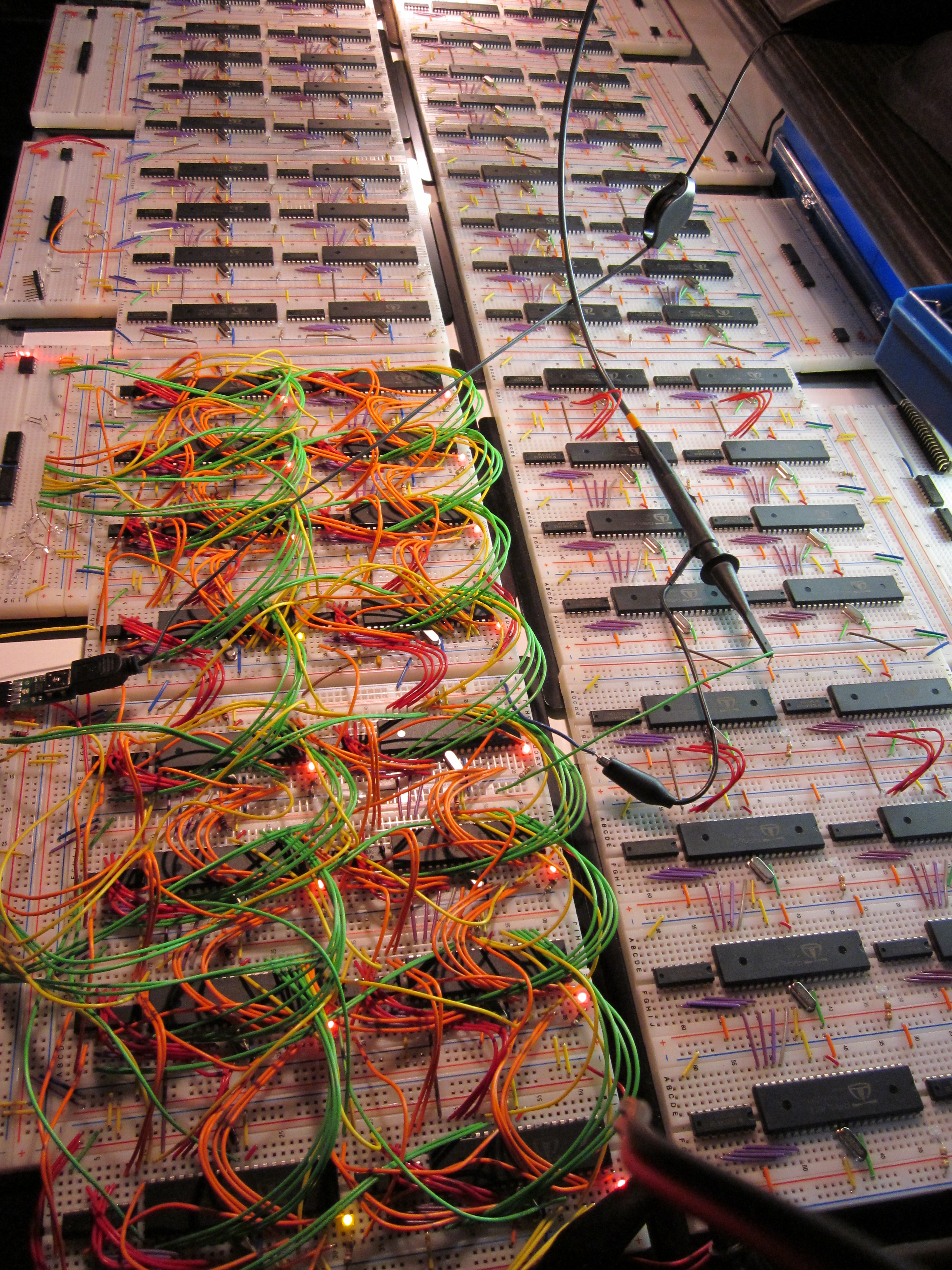
Breadboard
View on GrokipediaHistory
Early Prototyping Techniques
In the late 19th century, early telephone engineers relied on makeshift prototyping techniques to assemble and test circuits, often using wooden panels or boards as bases for mounting components such as receivers, transmitters, and switches with nails, screws, or carriage bolts.[11] These methods allowed for temporary connections via bare wires or terminal strips secured directly to the wood, facilitating experimentation with electromagnetic devices during the development of telephony systems.[9] The term "breadboard" emerged in the 1920s among radio hobbyists, who repurposed actual wooden kitchen breadboards—flat slabs traditionally used for cutting dough—as convenient platforms for point-to-point wiring of vacuum tube circuits.[12] Amateurs would nail or screw tube sockets, resistors, capacitors, and binding posts onto these boards, then interconnect them with insulated wire to build receivers and transmitters, enabling quick modifications without soldering.[8] This approach, popularized in amateur radio publications and kits, marked a shift toward accessible, non-permanent prototyping for personal and experimental electronics.[13] During the 1940s and 1950s, wartime demands for rapid electronics development, particularly in radar and communication systems, accelerated the evolution from permanent soldering to more flexible temporary assembly methods.[14] Engineers increasingly favored point-to-point wiring on insulated boards or wire-wrap techniques, which allowed circuits to be built, tested, and reconfigured swiftly to meet urgent military prototyping needs, reducing time and material waste compared to soldered prototypes.[10] This period laid the groundwork for later innovations in solderless prototyping.[9]Development of Solderless Breadboards
The development of solderless breadboards marked a significant advancement in electronic prototyping, enabling temporary circuit assembly without permanent connections like soldering. The foundational patent for such a device was granted to Orville I. Thompson of DeVry Technical Institute in 1963 for a filing made in 1960, describing a transparent insulating board with spring-biased contact jaws that grip inserted conductors to form circuits.[15] This design allowed for easy assembly and disassembly of experimental electrical apparatus, addressing the limitations of earlier methods that relied on fixed wiring.[15] The modern clip-based solderless breadboard, widely used today, was invented by Ronald J. Portugal while working for E&L Instruments Inc. in 1971.[16] Portugal's design featured a plastic board with rows of holes spaced at 0.1 inches (2.54 mm) to match integrated circuit pin spacing, interconnected internally by spring metal clips that securely hold component leads and wires without soldering.[17] This innovation was formalized in U.S. Design Patent D228,136, filed on December 1, 1971, and issued on August 14, 1973, assigning rights to E&L Instruments of Derby, Connecticut.[16] The patent emphasized the board's utility for rapid prototyping of electronic components, with a layout including central terminal strips for signal connections and peripheral bus strips for power distribution, facilitating complex circuit builds.[16] Commercialization began shortly after Portugal's invention, with E&L Instruments introducing the product line in the early 1970s under names like "Solderless Breadboard," making it accessible for educational, hobbyist, and professional use.[17] By the mid-1970s, other manufacturers adopted and refined the design, leading to widespread industry adoption as integrated circuits proliferated and prototyping demands grew.[18] Improvements in the late 1970s and 1980s focused on durability, with enhancements to contact materials (e.g., phosphor bronze springs for better conductivity and reliability) and board construction using high-impact ABS plastic, while standardizing power rails as integral full-length buses to simplify voltage distribution across larger prototypes.[19] These evolutions solidified the solderless breadboard's role as an essential tool in electronics development.[20]Design and Components
Terminal Strips and Power Buses
The central terminal strips form the core of a solderless breadboard's layout, consisting of multiple rows of five spring-loaded clips that are electrically interconnected horizontally within each row to facilitate component insertion and signal distribution.[3] These strips typically divide the board into two symmetrical sections separated by a central notch, allowing integrated circuits or components with multiple leads to straddle the gap while maintaining connections across up to five points per row.[21] Power buses, also known as distribution strips or rails, run vertically along the outer edges of the breadboard, providing dedicated paths for supplying positive voltage (+V) and ground to various parts of the circuit.[3] Each side usually features two such buses—one for power and one for ground—with the connections segmented into 25 or 50 discrete points per rail to match the board's row count, and often including a breakable jumper in the center to isolate the upper and lower halves for independent voltage distribution or board separation.[22] The breadboard's housing is constructed from durable ABS plastic for reusability and mechanical stability, while the internal spring clips are made of phosphor bronze or beryllium copper, typically nickel-plated, to ensure low-resistance, reliable electrical contacts generally rated for currents up to 1 A per connection at low voltages (such as 5 V), with a typical power limit of 5 W, though specifications vary by manufacturer.[23] Standard configurations include the 400-point layout, featuring 30 rows of 10 holes (five per side in the terminal strips) plus four 25-point power buses, and the larger 830-point layout with 63 rows of 10 holes plus four 50-point power buses, where tie-points are referenced by row numbers (e.g., 1–30 or 1–60) and column letters (e.g., A–E for one side, F–J for the other) to aid in circuit documentation and troubleshooting.[24][22] Jump wires can bridge between these fixed strips and buses for custom interconnections.[3]Interconnections and Jump Wires
Jump wires, also known as jumper wires or DuPont wires, are essential for creating temporary interconnections on solderless breadboards. These are pre-cut lengths of insulated solid-core wire, typically 22 AWG (American Wire Gauge), equipped with male pin connectors at one or both ends to fit securely into the breadboard's spring-loaded clips without requiring soldering.[25] The solid-core construction ensures reliable electrical contact and mechanical stability, as stranded wires can fray or fail to hold firmly in the clips.[26] They enable users to route signals, power, and ground between distant points on the breadboard or to external components. Common varieties include male-to-male (M/M) jumpers for linking breadboard holes directly, male-to-female (M/F) for connecting breadboard points to components with female headers, and female-to-female (F/F) for bridging modules or shields.[27] Lengths typically range from a few inches to several inches, allowing flexibility in circuit layout while minimizing clutter. Jump wires can also interface briefly with the breadboard's power buses to extend distribution to active components.[3] A standard color-coding convention simplifies circuit troubleshooting and assembly: red wires designate positive power connections (such as +5V or +3.3V), black wires indicate ground (GND), and other colors—such as yellow, green, blue, or white—are assigned to signal lines or data paths.[7] This practice, widely adopted in electronics prototyping, reduces errors by visually distinguishing functional roles.[28] To make connections, align the wire's pin with the target breadboard hole and insert it perpendicularly with gentle pressure until the insulation contacts the board's surface, ensuring the bare wire end engages the internal clip fully.[29] Avoid loose fits by selecting wires of the appropriate gauge (e.g., 22-24 AWG) and stripping insulation precisely to about 3-5 mm, as undersized or overly flexible wires may disconnect during handling.[30] Over-insertion should be prevented to avoid bending the wire or pushing it through to the underside, which could cause unintended shorts between adjacent rows or buses.[29] Proper technique involves routing wires above the board to prevent tangling and testing continuity with a multimeter after insertion. Accessories enhance organization in prototyping setups, including comprehensive jump wire kits with assorted lengths, colors, and connector types for quick access during assembly.[26] Wire dispensers or spools of bulk solid-core wire, paired with automatic strippers, allow custom cutting and preparation, promoting efficient and neat workflows in educational or hobbyist environments.[31]Variations in Size and Layout
Breadboards are available in a range of sizes to accommodate projects from simple circuits to more complex assemblies. The mini breadboard, typically featuring 170 tie points, measures approximately 47 mm × 35 mm and is ideal for compact prototypes involving up to two 14- or 16-pin DIP integrated circuits.[32] Half-size boards offer 400 tie points across 30 rows, with dimensions around 83 mm × 55 mm, suitable for small to medium projects.[24] Full-size variants provide 830 tie points in a 55 mm × 170 mm layout, supporting broader experimentation while maintaining standard 0.1-inch spacing.[33] For larger endeavors, jumbo boards extend to 3220 tie points, measuring about 185 mm × 190 mm, enabling extensive circuit layouts without multiple units.[34]| Size Variant | Tie Points | Approximate Dimensions (mm) | Typical Use |
|---|---|---|---|
| Mini | 170 | 47 × 35 | Compact prototypes with few ICs |
| Half-Size | 400 | 83 × 55 | Small to medium projects |
| Full-Size | 830 | 55 × 170 | General experimentation |
| Jumbo | 3220 | 185 × 190 | Large-scale assemblies |