Hubbry Logo
Complex programmable logic deviceComplex programmable logic deviceMain
Open search
Complex programmable logic device
Community hub
Complex programmable logic device
logo
8 pages, 0 posts
0 subscribers
Be the first to start a discussion here.
Complex programmable logic device
from Wikipedia
An Altera MAX 7000-series CPLD with 2500 gates in a PLCC package.
Die of an Altera EPM7032 EEPROM-based CPLD. Die size 3446x2252 μm. Technology node 1 μm.

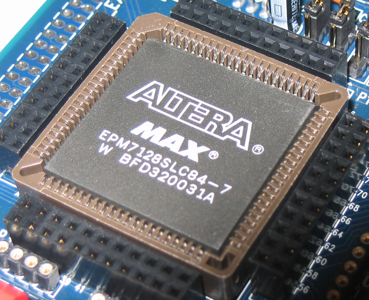
A complex programmable logic device (CPLD) is a programmable logic device with complexity between that of programmable array logic (PAL) and field-programmable gate arrays (FPGA), and architectural features of both. The main building block of the CPLD is a macrocell, which contains logic implementing disjunctive normal form expressions and more specialized logic operations.

Features

[edit]

Some of the CPLD features are in common with PALs:

  • Non-volatile configuration memory. Unlike many FPGAs, an external configuration ROM is not required, and the CPLD can function immediately on system start-up.
  • For many legacy CPLD devices, routing constrains most logic blocks to have input and output signals connected to external pins, reducing opportunities for internal state storage and deeply layered logic. This is usually not a factor for larger CPLDs and newer CPLD product families.

Other features are in common with FPGAs:

  • Large number of gates available. CPLDs typically have the equivalent of thousands to tens of thousands of logic gates, allowing implementation of moderately complicated data processing devices. PALs typically have a few hundred gate equivalents at most, while FPGAs typically range from tens of thousands to several million.
  • Some provisions for logic more flexible than sum-of-product expressions, including complicated feedback paths between macro cells, and specialized logic for implementing various commonly used functions, such as integer arithmetic.

The most noticeable difference between a large CPLD and a small FPGA is the presence of on-chip non-volatile memory in the CPLD, which allows CPLDs to be used for "boot loader" functions, before handing over control to other devices not having their own permanent program storage. A good example is where a CPLD is used to load configuration data for an FPGA from non-volatile memory.[1]

Distinctions

[edit]

CPLDs were an evolutionary step from even smaller devices that preceded them: programmable logic arrays (PLA) (first shipped by Signetics) and PALs. These in turn were preceded by standard logic products, which offered no programmability and were used to build logic functions by physically wiring several standard logic chips (or hundreds of them) together (usually with wiring on a printed circuit board or boards, but sometimes, especially for prototyping, using wire wrap wiring).

The main distinction between FPGA and CPLD device architectures is that CPLDs are internally based on a collection of PLDs accompanied by a programmable interconnection structure, while FPGAs use logic blocks.

See also

[edit]

References

[edit]
Revisions and contributorsEdit on WikipediaRead on Wikipedia
from Grokipedia
A Complex Programmable Logic Device (CPLD) is a programmable that combines multiple programmable logic blocks, known as macrocells, with a global programmable interconnect to implement custom digital logic functions, extending the capabilities of simpler programmable logic devices (PLDs) for higher-density applications. These devices typically feature sum-of-products logic derived from (PAL) architectures, enabling wide gates and predictable timing performance in a single chip. CPLDs emerged in the mid-1980s as an evolution from earlier PLDs, such as programmable logic arrays (PLAs) and PALs developed in the late 1970s, to address limitations in logic density and interconnect flexibility for increasingly complex designs. Pioneered by companies like Altera (now part of Intel), the first commercial CPLDs, such as the MAX series introduced in 1988, utilized erasable and reprogrammable technology using EEPROM or flash memory, allowing in-system programming (ISP) via standards like JTAG. This advancement enabled rapid prototyping and field updates, reducing development time and costs compared to fixed ASIC implementations. The core architecture of a CPLD consists of an array of macrocells—each capable of implementing combinational and through AND/OR planes and flip-flops—interconnected by a switch matrix or programmable routing resources that provide full connectivity without the hierarchical routing found in field-programmable gate arrays (FPGAs). This structure supports logic capacities from hundreds to about 10,000 gates, with features like dedicated clock lines and blocks for high-speed operations up to 200-300 MHz and low consumption under 100 μA in low-power variants. Unlike FPGAs, which use lookup tables (LUTs) for finer-grained logic and volatile SRAM configuration, CPLDs offer non-volatile storage, instant-on operation, and simpler timing models, making them ideal for , state machines, and control interfaces in cost-sensitive, low-to-medium complexity systems. As of 2025, CPLDs from manufacturers like Intel (MAX 10 series), Lattice Semiconductor (MachXO series), and Microchip (ATF/ATF150x series) continue to serve applications in telecommunications, automotive electronics, consumer devices, and industrial controls, where reliability, low power, and fast configuration times are critical; note that AMD discontinued its Xilinx CoolRunner CPLD line in 2024 due to declining demand. Recent trends include enhanced low-power designs for IoT and edge AI integration. Their design flow involves hardware description languages (HDLs) like VHDL or Verilog, synthesized using vendor-specific tools, emphasizing ease of integration and reduced board space over the scalability of larger FPGAs.

Overview

Definition and Purpose

A complex programmable logic device (CPLD) is a programmable that integrates multiple simple programmable logic device (SPLD) blocks, such as (PAL) or (PLA) structures, interconnected via a programmable routing matrix to implement moderately complex digital logic functions. These devices typically feature high-density macrocells—ranging from dozens to hundreds—enabling capacities up to several thousand gates, and are fabricated using technologies like or flash for configuration retention without power. The primary purpose of CPLDs is to provide a flexible, cost-effective alternative to custom application-specific integrated circuits () for implementing , interface bridging, and control functions in electronic systems, facilitating and changes through in-system reprogrammability. By supporting applications like I/O expansion, memory interfacing, and simple state machines, CPLDs reduce development time and board space compared to discrete logic components or full-scale field-programmable gate arrays (FPGAs), particularly in low-to-medium complexity scenarios where predictability and low power are essential. At their core, CPLDs operate by combining fixed macrocells—each containing flip-flops for and AND/OR planes for —with a global interconnect network that allows user-defined routing of signals between blocks, thereby realizing custom functions and state machines. This architecture ensures predictable timing performance due to the centralized interconnect, distinguishing CPLDs within the broader family of programmable logic devices as optimized for reliable, non-volatile operation in embedded systems.

Evolution from Simpler Devices

Complex programmable logic devices (CPLDs) represent a significant advancement over simple programmable logic devices (SPLDs), such as (PAL) structures, by integrating multiple SPLD-like logic blocks onto a single chip. This architecture addresses the primary limitation of SPLDs, which were restricted to small-scale implementations due to their fixed internal wiring and limited capacity for combining logic functions. By combining several such blocks, CPLDs enable the realization of more intricate digital circuits without requiring multiple discrete components. A pivotal development in this evolution occurred in the with the introduction of programmable interconnects, which provided flexible routing between the independent logic blocks. Unlike SPLDs, where interconnections were largely predetermined and inflexible, these programmable matrices allowed signals to be routed dynamically during configuration, facilitating larger designs while maintaining predictable timing performance. This innovation marked a shift toward scalable programmable logic, reducing the reliance on custom wiring and enabling efficient implementation of complex state machines and . In terms of scale, SPLDs typically support logic equivalent to up to 600 gates, suitable only for basic functions like glue logic. In contrast, CPLDs expand this to thousands of gates, offering a practical intermediate solution that bridges the gap to application-specific integrated circuits () for moderately complex systems requiring reprogrammability.

History

Early Development

The concept of the complex programmable logic device (CPLD) emerged in the late 1970s as researchers sought to extend the (PAL) architecture, introduced in 1978 by Monolithic Memories Inc., to support larger, more interconnected logic structures. This evolution addressed limitations in single-array devices by exploring multi-block configurations, allowing for greater logic capacity without relying on custom . Prototyping of the first CPLD-like devices occurred around 1983, coinciding with the founding of Corporation by engineers including Robert "Bob" Hartmann, who is credited as a key inventor of the company's initial programmable logic designs. Altera taped out its pioneering erasable programmable logic device (EPLD) by December 1983, marking a significant step toward CPLD implementation with reprogrammable logic arrays and interconnects. This prototype emulated multiple PAL functions in a single chip, demonstrating feasibility for complex logic integration. Hartmann held foundational patents for these early devices, emphasizing erasable and reconfigurable elements. In 1988, introduced the MAX (Multiple Array Matrix) architecture, which combined multiple logic arrays with a programmable interconnect matrix for enhanced density and flexibility. This innovation built on evolutionary roots in simpler programmable logic devices (SPLDs) by scaling their array-based design to handle more gates. Driving these efforts were broader VLSI advancements in the late 1970s and early 1980s, including shrinking transistor sizes enabled by and improved fabrication processes, which made higher-density programmable logic viable amid rising demands for customizable digital circuits.

Commercial Milestones

The first commercial complex programmable logic device (CPLD) was Altera's MAX 5000 series, introduced in 1988, which featured up to 32 macrocells and a programmable interconnect array based on the MAX architecture to enable higher logic density and flexibility over prior simple PLDs. Subsequent advancements came from with the ispLSI family launched in the early , offering high-density CPLDs with enhanced routing resources and performance for broader commercial adoption in digital systems. Other early contributors included with its ATF series in the late 1980s and with flash-based CPLDs in the . In 1997, entered the market with the XC9500 family, pioneering in-system programmability (ISP) using flash-based technology that allowed reconfiguration without specialized hardware, significantly improving prototyping and field updates while supporting up to 288 macrocells. By the , CPLD technology evolved toward greater integration, with devices like Intel's MAX 10 series incorporating , analog features, and non-volatile configuration for low-power applications. In 2025, advanced security features with the MachXO5-NX family, the industry's first post-quantum cryptography (PQC)-ready low-density FPGA/CPLD hybrid, enhancing protection against emerging threats in data centers and secure systems.

Architecture

Core Components

The core components of a complex programmable logic device (CPLD) form the foundational building blocks for implementing digital logic functions, enabling the device to serve as a versatile alternative to discrete logic in system designs. Macrocells serve as the basic units within a CPLD, each capable of realizing both combinational and sequential logic. Typically, a macrocell includes a programmable AND array that generates product terms from input signals, feeding into a fixed OR array to produce the sum-of-products output for combinational functions; this structure allows implementation of complex Boolean expressions. For sequential elements, macrocells incorporate configurable flip-flops, such as D-type, JK, T, or SR types, which provide storage and synchronization, often with dedicated controls for clock, reset, preset, and enable signals. Additionally, macrocells integrate I/O buffers to interface directly with external pins, supporting output driving and input reception. In the Altera MAX 7000 family, for instance, each macrocell features a programmable AND/fixed-OR array with five product terms and supports MultiVolt I/O buffers compatible with 3.3V and 5.0V standards. Logic array blocks (LABs) aggregate multiple macrocells to enhance logic capacity and efficiency, typically grouping 8 to 16 macrocells per block to mimic the of simpler programmable logic devices while scaling for . Within an LAB, macrocells share product terms through dedicated expanders, allowing efficient allocation of resources for wide combinational functions without excessive redundancy; for example, shareable expanders enable product terms to be borrowed across macrocells, optimizing logic utilization. This sharing mechanism supports up to 15 parallel expanders in some designs, facilitating broader input . In the Altera MAX 7000 architecture, each LAB contains 16 macrocells with 16 shareable expanders, promoting dense implementation of state machines and . Similarly, Lattice Semiconductor's ispMACH 4000V/Z family integrates macrocells into blocks with product-term sharing for high-performance applications. I/O blocks handle the external interfacing of the CPLD, providing configurable pins that can be allocated to macrocells for input, output, or bidirectional operation. These blocks include tri-state buffers for direction control and support multiple voltage standards to ensure compatibility with diverse systems, such as LVTTL for low-voltage TTL signaling. Pin allocation allows flexibility, where inputs can bypass macrocells for direct routing or use them for registered I/O, and bidirectional pins employ enable signals for tristate management. In the Altera MAX 7000 series, I/O blocks support up to 164 user I/O pins with LVTTL compatibility and global output enable signals (two or six per device) for bidirectional control. Lattice's ispMACH 4000V/Z devices feature 5V-tolerant I/Os supporting LVTTL, LVCMOS (at 3.3V, 2.5V, or 1.8V), and PCI 3.3 standards, with dedicated inputs enhancing connectivity.

Interconnect Structure

The interconnect structure in a complex programmable logic device (CPLD) primarily revolves around a central switch matrix that serves as the programmable wiring backbone, connecting macrocells, input/output (I/O) blocks, and other logic elements to enable flexible signal routing. This matrix typically employs pass transistors or multiplexers to selectively route signals, allowing any macrocell output to connect to any input or I/O pin within the device's capacity, which ensures predictable timing and high utilization in small to medium-scale designs. For instance, in the AMD Mach series, the central switch matrix routes all inter-block connections, ensuring predictable timing and high utilization. The routing architecture in CPLDs is generally fixed and hierarchical, featuring global lines that span the entire chip for long-distance signal propagation and local lines confined to specific logic blocks for shorter interconnections, which minimizes congestion and supports up to 100% utilization in designs with fewer than 500 macrocells. This structure contrasts with more segmented approaches in other devices by using a unified interconnect pool, such as the Programmable Interconnect Array (PIA) in Altera's MAX series or the global routing pool in Lattice's ispLSI family, where signals from macrocells feed into the pool and are distributed via multiplexers to designated destinations. The hierarchical channels, often comprising 32 to 36 true and complemented signals per block as in AMD's CoolRunner XPLA3 Zero-Power Interconnect Array (ZIA), enable efficient without excessive delay. Configuration of the interconnect is stored on-chip, typically in non-volatile EEPROM or flash memory for in-system reprogrammability without power loss, though some variants use volatile SRAM with battery backup or shadow EPROM for faster reconfiguration. In the Lattice ispMACH 4A family, for example, the central switch matrix configuration is loaded into EEPROM cells that control pass transistor states, allowing signals to be routed between product-term array blocks and I/O via an output switch matrix. This method ensures the routing remains intact across power cycles, supporting rapid prototyping and field updates in embedded applications.

Key Features

Programmability Aspects

Complex programmable logic devices (CPLDs) primarily employ non-volatile programming technologies such as electrically erasable programmable read-only memory (EEPROM) and flash memory to store configuration data, ensuring that the programmed logic persists without power. For instance, Lattice Semiconductor's ispMACH 4000 family utilizes EEPROM cells, which allow for unlimited reprogramming cycles while maintaining non-volatility through floating-gate transistor structures that retain charge states. Similarly, Intel's MAX II and MAX V CPLD families rely on flash-based configuration memory, where the configuration flash memory (CFM) block holds the bitstream in non-volatile flash cells, enabling reliable retention across power cycles without the need for external configuration devices. These technologies contrast with simpler PROM or EPROM used in earlier programmable logic, offering higher density and easier in-circuit erasure. CPLDs support high levels of reconfigurability through in-system programmability (ISP), which permits logic updates without removing the device from the circuit board, typically via the IEEE 1149.1 () boundary-scan interface. Intel's MAX II devices, for example, implement ISP using a four-pin port to access the CFM block, involving steps like entering ISP mode, sector erasure (up to 500 ms), programming (75 µs per address), and verification, all compliant with IEEE Std. 1149.1-2001 and IEEE 1532-2002 standards for secure, concurrent operation. This capability extends to real-time updates where new configurations load on the next power cycle, minimizing system downtime in deployed applications. Lattice CPLDs similarly leverage for ISP, supporting Jam STAPL or byte-code files to reprogram non-volatile elements directly in the field. Notable legacy CPLD families, such as AMD's CoolRunner-II and Xilinx's XC9500 series, featured fuse-based but were discontinued in 2023-2024, with end-of-life by 2027. To safeguard , CPLDs integrate features such as built-in fuses and mechanisms that deter reverse-engineering of proprietary logic designs. Lattice's MachXO3D family employs immutable hardware root-of-trust with 256-bit AES for bitstream protection, ensuring that encrypted configurations resist cloning or tampering during in-system updates. These features, often activated by blowing fuses, render the internal logic opaque to external probing, though they may limit reprogramming in some cases.

Performance Characteristics

Complex programmable logic devices (CPLDs) exhibit logic densities typically ranging from 600 to 10,000 equivalent gates, making them suitable for mid-scale digital designs that require more capacity than simple PLDs but less than large-scale FPGAs. This range allows CPLDs to implement functions involving hundreds of s, where each can handle complex combinational and , providing flexibility for and state machines without excessive resource overhead. For instance, devices like the MAX 7000 series offer up to 5,000 usable gates across 256 macrocells, balancing density with efficient routing in non-volatile architectures. Timing performance in CPLDs is characterized by propagation delays of 5 to 20 ns, enabling reliable operation in systems demanding quick response times. The fixed interconnect structure inherent to CPLD architectures ensures predictable timing, as signals traverse a centralized routing matrix rather than variable-length paths, minimizing and facilitating easier design verification compared to more configurable devices. System operating frequencies can reach up to 200 MHz, with counter speeds often cited at 100 to 175 MHz in commercial implementations, supporting applications like high-speed interfacing without the timing closure challenges of denser alternatives. Power consumption in CPLDs features low static power in the range of 0.02 to 50 mW, attributable to their non-volatile flash or storage that eliminates the need for external configuration memory and reduces leakage during idle states. Dynamic power, however, increases with and activity, potentially reaching tens of mW in fully utilized configurations due to switching in macrocells and I/O buffers, though overall profiles remain efficient for battery-powered or space-constrained systems. Manufacturers like Lattice report standby currents as low as 22 μW for devices such as the MachXO2 family, highlighting the trade-off where denser logic blocks elevate active consumption but maintain advantages in low-power scenarios enabled by programmable features.

Comparisons

With Simple Programmable Logic Devices

Complex programmable logic devices (CPLDs) represent an advancement over simple programmable logic devices (SPLDs) primarily in terms of scale and architectural flexibility, enabling the implementation of more intricate digital circuits. SPLDs, such as (GAL) devices, are typically confined to a single with fixed interconnects, supporting only a few hundred to around 1,000 logic gates and limited macrocells (usually 8–16), which restricts them to basic functions like glue logic for connecting discrete components in small-scale designs. In contrast, CPLDs incorporate multiple programmable logic blocks—often resembling interconnected PAL-like arrays—with programmable interconnect resources, scaling to thousands of macrocells (32–512) and up to 10,000 gates, allowing for distributed logic implementation across larger systems. This scalability leads to distinct use case divergences between the two. SPLDs excel in straightforward applications, such as basic address decoding or simple in low-complexity circuits like counters and binary adders, where their limited resources suffice without the overhead of additional interconnects. CPLDs, however, support more sophisticated designs, including finite state machines (FSMs), UART or SPI controllers, and address decoding in multi-component systems, leveraging their multi-block structure to manage timing and across broader interconnect fabrics. From a and perspective, SPLDs offer a more economical solution for designs with low gate counts, typically under 1,000 gates, due to their simpler architecture, lower power consumption, and basic programming tools like PALASM. For projects exceeding this threshold—such as those requiring over 100 gates—CPLDs provide superior by consolidating multiple SPLDs into a single device, reducing board space, component count, and overall system cost despite their higher per-unit price and need for advanced tools like Quartus.

With Field-Programmable Gate Arrays

Field-programmable gate arrays (FPGAs) and complex programmable logic devices (CPLDs) differ fundamentally in their architectural approaches, with FPGAs employing a fine-grained structure based on lookup tables (LUTs) and configurable logic blocks (CLBs) interconnected via extensive segmented routing channels to support millions of logic gates. In contrast, CPLDs utilize a coarser architecture consisting of multiple product-term-based macrocells, often derived from simple programmable logic device (SPLD) blocks like programmable array logic (PAL), connected through a global programmable interconnect array (PIA) that provides shared routing among macrocells. This LUT-based granularity in FPGAs enables greater flexibility for complex, register-intensive designs, while the product-term macrocells in CPLDs excel in combinatorial logic with wide fan-in capabilities, such as decoding functions, but limit scalability due to the centralized interconnect. Due to non-volatile memory technologies like or flash, CPLDs provide instant-on operation upon power-up with no configuration delay and support in-system reprogramming in seconds without external configuration devices, ensuring predictable timing from fixed interconnect paths. FPGAs, primarily SRAM-based, require loading configuration bitstreams from external memory upon power-up, incurring delays of milliseconds to seconds, though they support dynamic partial reconfiguration for targeted regions in microseconds to milliseconds and features like multi-boot to reduce overall startup time. This makes CPLDs suitable for applications demanding immediate startup and timing certainty with infrequent updates, whereas FPGAs offer greater flexibility for dynamic reconfiguration in compute-intensive systems despite variable routing paths and startup overhead. FPGAs achieve significantly higher logic densities, scaling to millions of gates for system-on-chip (SoC) implementations in high-volume production, but at greater cost per unit for small-scale designs due to their complex transistor-heavy fabrication. CPLDs, with densities typically up to tens of thousands of gates, offer lower costs for low- to medium-volume applications requiring predictable performance, as their simpler metal-optimized architecture reduces die size and manufacturing expenses. For instance, early high-capacity CPLDs like the Altera MAX 7000 provided around 5,000 usable gates at a fraction of the price of equivalent-density FPGAs, prioritizing glue logic over expansive compute tasks.

Applications

Digital System Integration

Complex programmable logic devices (CPLDs) play a crucial role in digital by functioning as , which connects disparate components such as microcontrollers, memories, and peripherals. This involves managing address decoding, signal synchronization, and bus arbitration to ensure seamless communication across the system. For instance, CPLDs facilitate interfacing with various memory types, including compact Flash and mobile SDRAM, while providing I/O expansion for up to 128 macrocells in certain architectures. A key aspect of this integration is CPLDs' ability to handle protocol conversions between different interfaces, enabling compatibility in mixed-signal environments. An example is bridging serial protocols like SPI (Serial Peripheral Interface) to I2S (Inter-IC Sound) for audio applications, where the CPLD acts as a master or slave to translate data formats, clocks, and control signals without requiring additional discrete components. Similar serial protocol conversions leverage the CPLD's programmable macrocells to buffer commands and data. In prototyping, CPLDs support for application-specific integrated circuits () by implementing control and interface logic rapidly, which shortens verification cycles and reduces time-to-market. They are often integrated into emulation hardware systems alongside FPGAs to handle peripheral interfacing and , allowing designers to test custom logic in real-time without full ASIC fabrication. This approach enables iterative modifications to system interfaces, accelerating development for complex designs. At the system level, CPLDs deliver significant benefits by consolidating multiple discrete integrated circuits (ICs) into a single programmable chip, thereby minimizing board space and simplifying layout. For example, a CPLD can replace numerous logic gates and drivers—such as those for LED control or PCI interfaces—significantly reducing the overall footprint while maintaining low power consumption. This integration not only cuts PCB complexity but also enhances reliability by eliminating solder joints associated with discrete parts.

Specific Industry Uses

In , CPLDs are employed for state machine control in routers and switches, enabling efficient packet routing logic through their programmable macrocells and interconnects that handle sequential operations and data flow management. These devices provide the necessary for interfacing communication protocols, supporting high-speed in network equipment where low latency and reliability are critical. Within the automotive sector, CPLDs facilitate interfacing and controllers in electronic control units (ECUs), processing inputs from environmental s and managing message arbitration on the CAN network for vehicle communication. Their non-volatile configuration and robust design ensure operation in harsh environments, including extreme temperatures, vibrations, and , making them suitable for safety-critical applications like engine management and advanced driver-assistance systems. Lattice Semiconductor's ispMACH series, for instance, supports automotive-grade reliability with low power consumption for such interfacing tasks. In , CPLDs serve as display controllers in televisions and appliances, generating timing signals and managing data for TFT-LCD panels to ensure smooth video rendering and interface compatibility. They also enable firmware updates by providing instant-on reconfiguration from embedded , allowing seamless over-the-air modifications without external processors. As of 2025, trends toward edge AI integration in smart appliances leverage CPLDs for control logic in low-power AI accelerators, handling and real-time decision-making in devices like connected TVs and systems. Intel's MAX series exemplifies this with high-performance, low-power features tailored for such consumer applications.

Design and Programming

Development Tools

Development tools for complex programmable logic devices (CPLDs) primarily encompass (EDA) software suites, integrated environments, and hardware programming interfaces, enabling engineers to capture, synthesize, verify, and configure designs targeting CPLD architectures. These tools are typically vendor-specific, optimized for particular device families such as Lattice's MachXO series or 's MAX series, and support both (HDL)-based and graphical entry methods to facilitate efficient prototyping and deployment. EDA software forms the core of CPLD development, providing comprehensive environments for design entry, synthesis, and place-and-route operations. For instance, Lattice Diamond offers a (GUI)-driven suite that supports HDL entry using , , and , alongside for mixed-signal and logic designs, with built-in synthesis engines like the Lattice Synthesis Engine (LSE) tailored for low-power CPLD implementations. Similarly, Intel's Quartus Prime Standard Edition provides robust support for CPLD design through , , and entry methods, including schematic editors for hierarchical design visualization, and integrates synthesis tools compatible with MAX II and MAX V CPLD families to optimize resource utilization and timing performance. These suites also incorporate constraint management tools, such as pin assignment editors and timing analyzers, to ensure designs meet interconnect and I/O specifications inherent to CPLD architectures. Simulation tools within these EDA environments enable functional and timing verification prior to hardware deployment, often featuring waveform viewers for signal analysis and debugging. Lattice Diamond integrates simulators like Siemens ModelSim or QuestaSim Lattice Edition, allowing users to create multi-file testbenches for behavioral simulation and post-synthesis timing checks, with support for mixed-language designs to validate CPLD-specific behaviors such as macrocell configurations. In Quartus Prime, simulation is handled through integrated ModelSim support or the native University Program VWF (Visual Waveform File) viewer, providing gate-level and RTL simulations with timing reports to identify critical paths in CPLD interconnect structures, ensuring reliable operation in targeted applications. These tools emphasize ease of setup via wizards, reducing verification time for iterative design cycles. Hardware programmers facilitate in-circuit configuration of CPLDs using standardized interfaces, primarily for boundary-scan access and compatibility with USB for host connectivity. Lattice provides the HW-USBN-2B USB download cable, a -compliant device that supports direct programming of multiple CPLDs in a , enabling non-volatile configuration of flash-based devices like the MachXO family with minimal board space requirements. For CPLDs, the USB Blaster cable serves as the primary programmer, integrated with the Quartus Prime Programmer tool to perform (ISP) of MAX series devices via USB 2.0 interfaces, supporting both volatile and modes for rapid field updates. These programmers ensure secure and efficient loading, often with features like voltage adaptation for diverse target boards.

Implementation Process

The implementation process for complex programmable logic devices (CPLDs) begins with the design flow, which transforms high-level descriptions into a physical configuration. Designers typically start by capturing the logic using hardware description languages (HDLs) such as VHDL or Verilog, followed by synthesis to generate a technology-independent netlist of gates and flip-flops optimized for the target CPLD architecture. This netlist is then processed through place-and-route (PnR) optimization, where the logic elements are mapped to the device's macrocells and interconnect resources, with algorithms balancing factors like routing congestion, signal delay, and resource utilization to meet performance goals. Timing analysis is integrated throughout, applying constraints to verify path delays and ensure the design operates within specified clock frequencies. The process culminates in bitstream generation, producing a configuration file—often in JEDEC format—that encodes the final routing and logic settings for the CPLD. Verification ensures reliability across stages, beginning with pre-synthesis using testbenches to validate functional against specifications. Post-route static timing analysis (STA) then examines the implemented design, checking setup and hold times for all paths, clock domain crossings, and margins (typically 10% for critical paths) to confirm timing closure without dynamic simulation overhead. These steps leverage vendor-provided tools in the ecosystem for iterative refinement until the design meets all constraints. Deployment involves programming the CPLD with the , commonly via boundary-scan (IEEE 1149.1 ) interfaces for in-system reconfiguration without device removal. For security-sensitive applications, options include bitstream encryption using AES-256 standards, where the configuration is encrypted with a user-defined key stored in , preventing unauthorized access or . Post-programming verification, such as validation, confirms successful loading.

References

Add your contribution
Related Hubs
User Avatar
No comments yet.