Hubbry Logo
Programmable Array LogicProgrammable Array LogicMain
Open search
Programmable Array Logic
Community hub
Programmable Array Logic
logo
8 pages, 0 posts
0 subscribers
Be the first to start a discussion here.
Contribute something
Programmable Array Logic
from Wikipedia
MMI 16R6 in 20-pin DIP
AMD 22V10 in 24-pin DIP

Programmable Array Logic (PAL) is a family of programmable logic device semiconductors used to implement logic functions in digital circuits that was introduced by Monolithic Memories, Inc. (MMI) in March 1978.[1] MMI obtained a registered trademark on the term PAL for use in "Programmable Semiconductor Logic Circuits". The trademark is currently held by Lattice Semiconductor.[2]

PAL devices consisted of a small PROM (programmable read-only memory) core and additional output logic used to implement particular desired logic functions with few components.

Using specialized machines, PAL devices were "field-programmable". PALs were available in several variants:

  • "One-time programmable" (OTP) devices could not be updated and reused after initial programming. (MMI also offered a similar family called HAL, or "hard array logic", which were like PAL devices except that they were mask-programmed at the factory.)
  • UV erasable versions (e.g.: PALCxxxxx e.g.: PALC22V10) had a quartz window over the chip die and could be erased for re-use with an ultraviolet light source just like an EPROM.
  • Later versions (PALCExxx e.g.: PALCE22V10) were flash erasable devices.

In most applications, electrically erasable GALs are now deployed as pin-compatible direct replacements for one-time programmable PALs.

History

[edit]

Before PALs were introduced, designers of digital logic circuits would use small-scale integration (SSI) components, such as those in the 7400 series TTL (transistor-transistor logic) family; the 7400 family included a variety of logic building blocks, such as gates (NOT, NAND, NOR, AND, OR), multiplexers (MUXes) and demultiplexers (DEMUXes), flip-flops (D-type, JK, etc.) and others. One PAL device would typically replace dozens of such "discrete" logic packages, so the SSI business declined as the PAL business took off. PALs were used advantageously in many products, such as minicomputers, as documented in Tracy Kidder's best-selling book The Soul of a New Machine.

PALs were not the first commercial programmable logic devices; Signetics had been selling its field programmable logic array (FPLA) since 1975. These devices were completely unfamiliar to most circuit designers and were perceived to be too difficult to use. The FPLA had a relatively slow maximum operating speed (due to having both programmable-AND and programmable-OR arrays), was expensive, and had a poor reputation for testability. Another factor limiting the acceptance of the FPLA was the large package, a 600-mil (0.6", or 15.24 mm) wide 28-pin dual in-line package (DIP).

The project to create the PAL device was managed by John Birkner and the actual PAL circuit was designed by H. T. Chua.[3] In a previous job (at mini-computer manufacturer Computer Automation), Birkner had developed a 16-bit processor using 80 standard logic devices. His experience with standard logic led him to believe that user-programmable devices would be more attractive if the devices were designed to replace standard logic. This meant that the package sizes had to be more typical of the existing devices, and the speeds had to be improved. MMI intended PALs to be a relatively low cost (sub $3) part. However, the company initially had severe manufacturing yield problems[citation needed] and had to sell the devices for over $50.[citation needed] This threatened the viability of the PAL as a commercial product, and MMI was forced to license the product line to National Semiconductor.[citation needed] PALs were later "second sourced" by Texas Instruments and Advanced Micro Devices.

Process technologies

[edit]

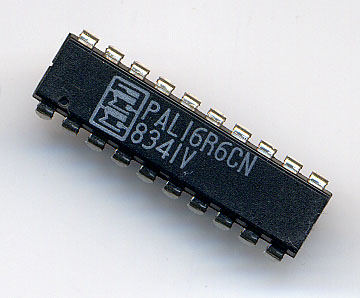
Early PALs were 20-pin DIP components fabricated in silicon using bipolar transistor technology with one-time programmable (OTP) titanium-tungsten programming fuses.[4] Later devices were manufactured by Cypress, Lattice Semiconductor and Advanced Micro Devices using CMOS technology.

The original 20- and 24-pin PALs were denoted by MMI as medium-scale integration (MSI) devices.

PAL architecture

[edit]
The programmable elements (shown as a fuse) connect both the true and complemented inputs to the AND gates. These AND gates, also known as product terms, are ORed together to form a sum-of-products logic array.

The PAL architecture consists of two main components: a logic plane and output logic macrocells.

Programmable logic plane

[edit]

The programmable logic plane is a programmable read-only memory (PROM) array that allows the signals present on the device pins, or the logical complements of those signals, to be routed to output logic macrocells.

PAL devices have arrays of transistor cells arranged in a "fixed-OR, programmable-AND" plane used to implement "sum-of-products" binary logic equations for each of the outputs in terms of the inputs and either synchronous or asynchronous feedback from the outputs.

Output logic

[edit]

The early 20-pin PALs had 10 inputs and 8 outputs. The outputs were active low and could be registered or combinational. Members of the PAL family were available with various output structures called "output logic macrocells" or OLMCs. Prior to the introduction of the "V" (for "variable") series, the types of OLMCs available in each PAL were fixed at the time of manufacture. (The PAL16L8 had 8 combinational outputs, and the PAL16R8 had 8 registered outputs. The PAL16R6 had 6 registered and 2 combinational outputs, while the PAL16R4 had 4 of each.) Each output could have up to 8 product terms (effectively AND gates); however, the combinational outputs used one of the terms to control a bidirectional output buffer. There were other combinations that had fewer outputs with more product terms per output and were available with active high outputs ("H" series).[5]: 1–14  The "X" series of devices had an XOR gate before the register.[5]: 1–9  There were also similar 24-pin versions of these PALs.

This fixed output structure often frustrated designers attempting to optimize the utility of PAL devices because output structures of different types were often required by their applications. (For example, one could not get 5 registered outputs with 3 active high combinational outputs.) So, in June 1983 AMD introduced the 22V10, a 24-pin device with 10 output logic macrocells.[6] Each macrocell could be configured by the user to be combinational or registered, active high or active low. The number of product terms allocated to an output varied from 8 to 16. This one device could replace all of the 24-pin fixed function PAL devices. Members of the PAL "V" ("variable") series included the PAL16V8, PAL20V8 and PAL22V10.

Programming PALs

[edit]

PALs were programmed electrically using binary patterns (as JEDEC ASCII/hexadecimal files) and a special electronic programming system available from either the manufacturer or a third party, such as DATA I/O. In addition to single-unit device programmers, device feeders and gang programmers were often used when more than just a few PALs needed to be programmed. (For large volumes, electrical programming costs could be eliminated by having the manufacturer fabricate a custom metal mask used to program the customers' patterns at the time of manufacture; MMI used the term "hard array logic" (HAL) to refer to devices programmed in this way.)

Programming languages (by chronological order of appearance)

[edit]
PALASM design of a 4-bit counter

Though some engineers programmed PAL devices by manually editing files containing the binary fuse pattern data, most opted to design their logic using a hardware description language (HDL) such as Data I/O's ABEL, Logical Devices' CUPL, or MMI's PALASM. These were computer-assisted design (CAD) (now referred to as "electronic design automation") programs which translated (or "compiled") the designers' logic equations into binary fuse map files used to program (and often test) each device.

PALASM

[edit]

The PALASM (from "PAL assembler") language was developed by John Birkner in the early 1980s and the PALASM compiler was written by MMI in FORTRAN IV on an IBM 370/168. MMI made the source code available to users at no cost. By 1983, MMI customers ran versions on the DEC PDP-11, Data General NOVA, Hewlett-Packard HP 2100, MDS800 and others.

It was used to express Boolean equations for the output pins in a text file, which was then converted to the 'fuse map' file for the programming system using a vendor-supplied program; later the option of translation from schematics became common, and later still, 'fuse maps' could be 'synthesized' from an HDL (hardware description language) such as Verilog.

CUPL

[edit]

Assisted Technology released CUPL (Compiler for Universal Programmable Logic) in September 1983.[7] The software was always referred to as CUPL and never the expanded acronym. It was the first commercial design tool that supported multiple PLD families. The initial release was for the IBM PC and MS-DOS, but it was written in the C programming language so it could be ported to additional platforms.[8] Assisted Technology was acquired by Personal CAD Systems (P-CAD) in July 1985. In 1986, PCAD's schematic capture package could be used as a front end for CUPL.[9] CUPL was later acquired by Logical Devices and is now owned by Altium.[10] CUPL is currently available as an integrated development package for Microsoft Windows.[11]

Atmel releases for free WinCUPL (their own design software for all Atmel SPLDs and CPLDs). Atmel was acquired by Microchip in 2016.

ABEL

[edit]

Data I/O Corporation released ABEL in April, 1984. The development team was Michael Holley, Mike Mraz, Gerrit Barrere, Walter Bright, Bjorn Freeman-Benson, Kyu Lee, David Pellerin, Mary Bailey, Daniel Burrier and Charles Olivier.

Data I/O spun off the ABEL product line into an electronic design automation company called Synario Design Systems and then sold Synario to MINC Inc in 1997. MINC was focused on developing FPGA development tools. The company closed its doors in 1998 and Xilinx acquired some of MINC's assets including the ABEL language and tool set. ABEL then became part of the Xilinx Webpack tool suite. Now Xilinx owns ABEL.

Device programmers

[edit]

Popular device programmers included Data I/O Corporation's Model 60A Logic Programmer and Model 2900.

One of the first PAL programmers was the Structured Design SD20/24. They had the PALASM software built-in and only required a CRT terminal to enter the equations and view the fuse plots. After fusing, the outputs of the PAL could be verified if test vectors were entered in the source file.

Successors

[edit]

After MMI succeeded with the 20-pin PAL parts introduced circa 1978, AMD introduced the 24-pin 22V10 PAL with additional features. After buying out MMI (circa 1987), AMD spun off a consolidated operation as Vantis, and that business was acquired by Lattice Semiconductor in 1999.[12]

Altera introduced the EP300 (first CMOS PAL) in 1983 and later moved into the FPGA business.

Lattice Semiconductor introduced the generic array logic (GAL) family in 1985, with functional equivalents of the "V" series PALs that used reprogrammable logic planes based on EEPROM (electrically eraseable programmable read-only memory) technology. National Semiconductor was a second source for GAL parts.

AMD PALCE 20V8H-15JC in 28-pin PLCC

AMD introduced a similar family called PALCE. In general one GAL part is able to function as any of the similar family PAL devices. For example, the 16V8 GAL is able to replace the 16L8, 16H8, 16H6, 16H4, 16H2 and 16R8 PALs (and many others besides).

ICT (International CMOS Technology) introduced the PEEL 18CV8 in 1986. The 20-pin CMOS EEPROM part could be used in place of any of the registered-output bipolar PALs and used much less power.

Larger-scale programmable logic devices were introduced by Atmel, Lattice Semiconductor, and others. These devices extended the PAL architecture by including multiple logic planes and/or burying logic macrocells within the logic plane(s). The term complex programmable logic device (CPLD) was introduced to differentiate these devices from their PAL and GAL predecessors, which were then sometimes referred to as simple programmable logic devices (SPLDs).

Another large programmable logic device is the field-programmable gate array (FPGA). These are devices currently[when?] made by Intel (who acquired Altera) and Xilinx (who was acquired by AMD) and other semiconductor manufacturers.

See also

[edit]

References

[edit]

Further reading

[edit]
Revisions and contributorsEdit on WikipediaRead on Wikipedia
from Grokipedia
Programmable Array Logic (PAL) is a type of (PLD) that enables the implementation of custom functions through a field-programmable AND gate array whose outputs connect non-programmably to a fixed OR gate array, allowing for efficient realization of sum-of-products expressions with reduced complexity compared to fully programmable alternatives. Invented by John Birkner and Hua-Thye Chua at Monolithic Memories Inc. (MMI), the first PAL device, such as the 16L8, was introduced in as a streamlined that traded some flexibility of Programmable Logic Arrays (PLAs) for faster delays and lower costs by limiting programmability to a single AND plane. This bipolar technology supported user programming via fuse-based methods and was accompanied by design tools like PALASM, facilitating easier entry into custom digital . PALs quickly became an industry standard for prototyping and small-scale production of logic circuits, influencing the development of subsequent devices like (GAL) in the 1980s and serving as a foundational precursor to modern field-programmable gate arrays (FPGAs).

Overview

Definition and Core Principles

Programmable Array Logic (PAL) is a family of devices classified as programmable logic devices (PLDs) designed to implement user-defined functions and limited through the selective programming of fusible links within an . These devices enable designers to customize digital circuits by configuring interconnections in a predefined array structure, allowing for the realization of expressions without the need for full custom fabrication. At the core of PAL operation is a two-level AND-OR logic structure, consisting of a programmable AND plane followed by a fixed OR plane, which inherently supports the implementation of logic functions in sum-of-products (SOP) form. In the AND plane, fusible links—typically thin metal fuses—are either left intact or blown open during programming to connect input signals (and their complements) to form product terms, with the programmable AND plane generating multiple such individual product terms that feed into the fixed OR plane; each OR gate sums a fixed number of these product terms (e.g., 2 to 8 per output) to produce each output, ensuring a structured yet flexible realization of combinational logic; for sequential applications, output macrocells may incorporate flip-flops driven by the OR outputs, with feedback paths to the AND plane for state-dependent logic. This architecture offers key advantages in simplicity, speed, and cost-effectiveness for implementing small to medium-scale logic functions, particularly when compared to custom application-specific integrated circuits (), as require no mask changes or lengthy fabrication cycles and support in low- to medium-volume production. The fixed OR plane reduces complexity and silicon area relative to fully programmable alternatives, enhancing propagation delays (often in the range) while maintaining predictability in timing analysis. A basic block diagram of a PAL illustrates inputs buffered to provide true and complemented signals feeding into the programmable AND , where fusible links define connections to multiple AND gates; the outputs of these AND gates connect via fixed wiring to OR gates in the OR , whose results drive output buffers or optional flip-flops in macrocells, forming a compact representation of SOP logic with feedback for sequential elements. Programmable Array Logic (PAL) devices differ from Programmable Logic Arrays (PLAs) primarily in their internal structure, where PALs feature a programmable AND array followed by a fixed OR array, enabling simpler and faster implementation of sum-of-products logic at the cost of reduced flexibility compared to PLAs' fully programmable AND and OR arrays. This fixed OR structure in PALs limits the sharing of product terms across outputs, making them more suitable for irregular or dedicated logic functions rather than the regular, highly optimized sum-of-products expressions that PLAs handle efficiently. In terms of density and complexity, PALs typically support 10 to 20 product terms per output with limited to around 10-16 inputs, whereas PLAs can accommodate higher term counts and broader / due to their dual programmability, though this increases area and propagation delay. In contrast to PROMs, which employ a fixed AND array (essentially a decoder) paired with a programmable OR array for memory-like operations, PALs invert this by programming the AND array to generate specific product terms while using a predefined OR array for output , allowing PALs to implement custom beyond simple table-based functions. PROMs excel in applications requiring exact address-to-data mapping, such as code conversion or state decoding, but lack the AND-plane customization that makes PALs versatile for in digital systems. Both are one-time programmable via fuse blowing, but PALs offer greater logic density for non-memory tasks, with typical devices handling 6-8 outputs versus PROMs' focus on wider bit storage. PALs also contrast with (GAL) devices, which extend the PAL architecture by incorporating EEPROM-based reprogrammability and programmable output macrocells that include flip-flops and XOR gates for support, addressing PALs' limitations in reusability and output configuration. While PALs use one-time programming via fuses and have fixed output macrocell configurations that support limited via flip-flops, GALs enable iterative design prototyping and more flexible registered outputs, though they maintain the fixed OR array for compatibility. Functionally, GALs suit evolving designs in prototyping, whereas PALs target fixed-production with lower cost per unit.
DeviceAND ArrayOR ArrayProgrammabilityTypical Density (Terms/Output)Primary Applications
FixedProgrammableOne-time (fuses)N/A (lookup-based)Memory, decoding
PLAProgrammableProgrammableOne-time (fuses)20+Flexible SOP logic
PALProgrammableFixedOne-time (fuses)10-20Irregular combinational logic
GALProgrammableFixedReprogrammable ()10-20Prototyping, sequential glue logic

History

Invention and Early Development

The invention of Programmable Array Logic (PAL) emerged in the mid-1970s at Monolithic Memories Inc. (MMI), driven by the need to simplify and reduce the cost of programmable logic devices for implementing combinational and sequential functions in digital circuits. Engineers John M. Birkner and Hua-Thye Chua led the development, conceptualizing PAL as a more efficient alternative to existing programmable logic arrays (PLAs) and field programmable logic arrays (FPLAs), which suffered from high complexity due to dual programmable planes (AND and OR arrays) that increased chip size, manufacturing costs, and design overhead. Early work began around , focusing on prototypes that retained a single programmable AND while fixing the connections to a dedicated OR , thereby enabling user-defined logic with fewer resources and greater predictability for simpler applications like glue logic in systems. These prototypes addressed PLA limitations by prioritizing fixed OR plane wiring, which eliminated the need for programmable interconnections in that section and reduced the risk of routing congestion, while incorporating features like output registers and feedback paths to support state machines and arithmetic operations. Development emphasized compatibility with standard TTL logic levels to facilitate integration into existing bipolar-based designs. The foundational concept was formalized in US Patent 4,124,899, titled "Programmable array logic circuit," filed on May 23, 1977, by Birkner and Chua and assigned to MMI. The patent detailed the PAL architecture as an evolution of FPLAs, highlighting its use of fusible links for one-time programming and bidirectional I/O pins for flexible pin assignments, which enhanced usability without compromising performance. Initial challenges during prototyping centered on bipolar transistor technology constraints, including higher power dissipation compared to later approaches and the reliability of titanium-tungsten fusible links for field programming, which required precise control to avoid over-programming or incomplete isolation of unused paths. MMI's efforts also grappled with balancing user programmability—allowing engineers to customize devices on-site using simple programmers—against the era's limitations in testing and verification tools for complex logic verification. These hurdles were overcome through iterative bipolar fabrication processes, paving the way for PAL's viability as a practical tool for .

Commercialization and Adoption

The first commercial Programmable Array Logic (PAL) device, the PAL16L8, was introduced by Monolithic Memories Inc. (MMI) in 1978 as a 20-pin bipolar designed for implementing custom functions. This device marked a significant advancement over earlier programmable logic arrays by simplifying the architecture with a programmable AND array feeding a fixed OR array, enabling faster design cycles and reduced prototyping costs for engineers. MMI's PAL family quickly became the standard for small-scale custom logic, with the PAL16L8 serving as the foundational model that supported up to 8 outputs and 10 inputs, programmable via fusible links. PAL devices saw rapid adoption throughout the late 1970s and 1980s, particularly in and applications where flexible, low-volume custom logic was essential. They were integrated into arcade video games for address decoding and control signal generation, such as in Konami's Scramble system, providing a cost-effective alternative to full custom ASICs. In early peripherals and systems like the Memotech MTX series, PALs handled and timing functions, contributing to the proliferation of personal . Their use extended to calculators and other portable devices, where space and power constraints favored programmable solutions over discrete gates. The devices' ease of programming via tools like PALASM further accelerated their uptake, allowing designers to replace hundreds of discrete TTL chips with a single PAL. The industry's embrace of PAL technology led to key standardization efforts by the Joint Electron Device Engineering Council (), which established pinout conventions and the JESD3 fuse map format in the early to ensure compatibility across manufacturers and programmers. This standardization, detailed in JEDEC publications, promoted widespread interoperability and reduced design risks for users. Following MMI's acquisition by in 1987 amid financial pressures in the semiconductor market, competition expanded as AMD and emerging players like produced second-source and enhanced PAL-compatible devices, further driving . A pivotal development in the was the introduction of CMOS-based PAL variants by MMI and around 1983, which offered significantly lower power dissipation—often below 100 mW—compared to bipolar versions, enabling broader use in battery-operated consumer products and extending the technology's relevance into the mid-1980s.

Architecture

Programmable AND-OR Array

The programmable AND-OR array forms the core logic plane of Programmable Array Logic (PAL) devices, enabling the implementation of functions through a structured of gates. It consists of an array of AND gates whose inputs are derived from the device's primary inputs and their logical complements, with connections established via fusible links that can be selectively opened during programming. These fusible links, typically implemented using bipolar fuse technology such as titanium-tungsten structures, allow each AND gate to form a product term by including or excluding specific input signals. The AND array is followed by a fixed OR array, where each output is the sum of a predetermined number of product terms from the AND gates, usually ranging from 2 to 8 terms per output in early devices. In operation, programming the AND array involves blowing selected fusible links to configure the connections, thereby defining the product terms as minterms or more general products of inputs. For instance, an unblown fuse connects an input to an AND gate, contributing a logic 1 factor, while a blown fuse isolates it, effectively multiplying by 0 and excluding that input from the term. The fixed OR array then performs a logical OR on the enabled product terms to generate each output signal, supporting the standard sum-of-products (SOP) form for Boolean functions. This architecture allows PAL devices to realize any combinational logic function that fits within the array's dimensions, such as decoders or multiplexers, by mapping the desired SOP equations to the available AND and OR resources. A representative example is the implementation of a 4-input XOR function, which computes the parity (odd number of high inputs) in SOP form: F=(1,2,4,7,8,11,13,14)F = \sum (1,2,4,7,8,11,13,14), where the minterms correspond to input combinations with an odd number of 1s (e.g., ABCD+ABCD+A'B'C'D + A'B'CD' + \dots). This requires 8 product terms, each formed by programming the AND array to select the appropriate literals from the 4 inputs and their complements, with the fixed OR array summing them for the single output; such a function fits within devices like the PAL16 series, which provide up to 7-8 terms per output. The SOP expansion ensures compatibility with the AND-OR structure, though more complex functions may require multiple macrocells if term counts exceed the limit. Key limitations of the programmable AND-OR array include the absence of feedback paths within the logic plane, restricting it to combinational-only implementations without sequential elements, and a fixed number of inputs—typically 16 in the PAL16 family (10 dedicated plus 6 bidirectional)—which bounds the complexity of addressable functions. These constraints prioritize density and speed in custom logic but necessitate careful function partitioning for larger designs.

Output Logic and Macrocells

In Programmable Array Logic (PAL) devices, the fixed OR plane serves as the non-programmable component that sums selected product terms from the preceding AND array to generate sum-of-products expressions for each output. This array typically connects a fixed number of inputs—often 6 to 8 per , depending on the device family—to form the logical OR function, enabling efficient implementation of without the complexity of a fully programmable OR structure. For instance, in early devices like the PAL16R4, each of the four outputs receives up to 8 product terms via dedicated , while more advanced variants such as the PAL22V10 allow variable distribution averaging 12 terms across 10 outputs, with a range of 8 to 16 to optimize resource allocation. The core of PAL output functionality resides in the , a versatile block associated with each output pin that integrates the output with configurable logic elements for enhanced flexibility. Each macrocell typically includes a D-type flip-flop for sequential operations, multiplexers for mode selection, and control fuses to define behavior, allowing outputs to be configured as combinational (bypassing for direct logic), registered (using the flip-flop for state storage), or in some variants latched for edge-triggered applications. Polarity control is a key feature, programmable via dedicated fuses (e.g., S0 for active-high or active-low inversion) to accommodate various logic requirements without external inverters. In the PAL22V10, for example, the macrocell's select lines (S1 and S0) enable four primary modes: registered active-low (S1=0, S0=0), registered active-high (S1=0, S0=1), combinational active-low (S1=1, S0=0), or combinational active-high (S1=1, S0=1), with feedback paths routed back to the AND array from either the OR output or the flip-flop Q-bar. Output options in PAL macrocells often incorporate tri-state buffers to support bus-oriented interfacing, where the buffer can be enabled or disabled via a dedicated product term or control pin, placing the output in a high-impedance state when not active. This allows multiple devices to share lines efficiently, as seen in the PAL16R8 where tri-state control is tied to pin 11 or individual terms, and in the PAL22V10 where each output has programmable enable logic. The macrocell block generally comprises the feeding a that selects between registered and combinational paths, followed by a polarity inverter and tri-state driver, with synchronous preset and asynchronous reset options for reliable initialization in sequential designs. As a representative example, configuring a macrocell in a PAL22V10 for a simple counter output involves setting it to registered mode (S1=0) with active-high polarity (S0=1), where the OR gate sums product terms representing the next-state logic (e.g., Q_n+1 = Q_n XOR clock_enable), clocked by the global CLK input, and feedback from the flip-flop Q to the AND array enables state retention across cycles. This setup, common in 4-bit counter implementations, leverages the macrocell's D flip-flop for toggle behavior while the tri-state buffer allows the output to interface with a shared bus when enabled.

Fabrication and Variants

Process Technologies

Programmable Array Logic (PAL) devices were initially fabricated using bipolar transistor-transistor logic (TTL) processes with clamping, introduced by Monolithic Memories Inc. (MMI) in 1978. This technology provided operation with propagation delays of 25-45 ns and clock frequencies up to 20 MHz in early variants like the 16L8, but it consumed significant power, with maximum dissipation of 700-1000 mW (140-210 mA at 5 V) due to the inherent characteristics of bipolar junctions. Programming in these bipolar PALs relied on one-time programmable (OTP) fusible links made from , which were electrically blown using 10.5-11.5 V pulses over 10-50 µs to open specific connections in the AND-OR array. Later bipolar variants used titanium-tungsten links. The industry began transitioning to complementary metal-oxide-semiconductor (CMOS) processes for PAL devices in 1983, starting with Altera's EP300 as the first CMOS PAL, driven by demands for reduced power consumption and increased logic density. Monolithic Memories Inc. (MMI) and Advanced Micro Devices (AMD), which acquired MMI in 1987, developed the PALCE series in the mid-1980s. CMOS PALs achieved power dissipation as low as 55 mA (275 mW) at 15 MHz operation, a substantial improvement over bipolar's higher quiescent currents, while enabling higher integration through more efficient transistor scaling and lower leakage. Variants incorporated electrically erasable programmable read-only memory (EEPROM) cells for reprogrammability or laser etching for permanent links, allowing up to 100 erase/program cycles in EEPROM-based designs before endurance limits. Lattice Semiconductor also contributed with generic array logic (GAL) devices in 1985, offering EEPROM-based reprogrammable CMOS alternatives. Process scaling for evolved from approximately 5-micron feature sizes in early bipolar implementations to sub-micron nodes (e.g., 0.8 µm) by the early in variants, facilitated by advances in and isolation techniques like IMOX-III slot isolation. This progression improved device speed to maximum clock frequencies (fMAX) of up to 50 MHz and supported standard pin counts of 20 to 28 pins in DIP and PLCC packages, balancing performance with compatibility for TTL/ logic levels. While OTP configurations remained dominant for cost-sensitive production, early reprogrammable attempts using UV-erasable or methods laid groundwork for flexible prototyping, though limited by cycle counts and security features like design protection bits.

Device Families and Specifications

Programmable Array Logic (PAL) devices follow a standardized that encodes key architectural and performance characteristics. The typical format is PALnXm, where n represents the number of inputs to the AND array (often equal to the total pins minus dedicated outputs and power pins, such as 16 or 20), X indicates the output configuration (e.g., L for combinatorial active-low outputs, R for registered outputs with flip-flops, V for versatile macrocells supporting both combinational and registered modes, or X for XOR-capable outputs), and m denotes the number of outputs (commonly 4, 6, 8, or 10). Suffixes further specify speed (e.g., -10 for 10 ns delay), power variants (e.g., H for half-power), temperature range (C for commercial 0°C to 70°C, M for -55°C to 125°C), and package type (e.g., PC for plastic DIP). For instance, the PAL16R4 features 16 inputs, 4 registered outputs, and is available in variants like PAL16R4-15PC for 15 ns commercial operation. Early PAL families were predominantly bipolar, leveraging TTL-compatible Schottky technology for high-speed applications. Representative bipolar devices include the PAL16L8 (16 inputs, 8 combinatorial outputs) and PAL20L8 (20 inputs, 8 combinatorial outputs), both introduced by Monolithic Memories Inc. in the late 1970s and widely adopted for replacing discrete TTL logic in interfaces and decoders. These devices typically feature 20- or 24-pin packages with 8-10 bidirectional I/Os, fixed OR-array product terms per output (e.g., 7-10 terms), and pin-compatible footprints across manufacturers like and TI to facilitate second-sourcing. Bipolar PALs offered propagation delays of 15-25 ns, enabling clock rates up to 20-40 MHz in sequential designs, though at higher power consumption levels. Early 1978 devices had slower 25-45 ns delays. CMOS-based PAL families emerged in the to address power efficiency, with the series from representing a key evolution. Devices like the PALCE22V10 (22 inputs, 10 versatile outputs) became industry standards, supporting in-system reprogrammability via cells and maintaining pin compatibility with bipolar predecessors in 24-pin packages. These variants typically provide 8-12 outputs with programmable product terms (up to 12 per ), propagation delays of 10-25 ns, and significantly lower power dissipation compared to bipolar counterparts. For example, the PALCE16V8 operates at 10-20 ns with standby currents as low as 100 µA in low-power modes.
Family TypeExample DevicePin CountOutputsPropagation Delay (ns)Power Dissipation (mW, typ. at 5V)Key Variants
BipolarPAL16L820815-25250-600High-speed (-7/-10), Low-power (-2), Commercial/
BipolarPAL20L824815-25300-600High-speed (-7), Low-power (L), Commercial/
CMOSPALCE16V820810-2550-275Half-power (H), Low standby (Z), Commercial/
CMOSPALCE22V10241010-25100-300Versatile (V), Speed-optimized (-10), Commercial/
Variants across families emphasize trade-offs in performance and environment. High-speed grades (e.g., -7 or -10 suffixes) achieve 7.5-10 ns delays for demanding applications like high-frequency counters, while low-power options (L or H) reduce dissipation by 50% or more through optimized Schottky or processes, suitable for battery-operated systems. Commercial grades dominate prototyping and , whereas military grades include extended temperature testing and hermetic packaging for and defense uses, ensuring reliability under extreme conditions. These specifications, enabled by evolving bipolar and process technologies, established PALs as versatile building blocks for custom logic integration.

Programming

Programming Mechanisms

Programmable Array Logic (PAL) devices primarily employ bipolar fuse technology for configuration, utilizing fusible links made from materials such as titanium-tungsten (Ti-W) or platinum-silicide (PtSi) in a Schottky TTL process. These links are initially intact, representing a logic 1 connection, and are selectively blown to create open circuits (logic 0) by applying high-current pulses through the desired paths. The blowing process involves raising the supply voltage (VCC) to 11.5–12 V and applying pulses of 10–50 µs duration at currents up to 50 mA on output pins, while other inputs are held at approximately 10 mA, ensuring precise targeting of individual fuses without affecting adjacent links. In CMOS variants of PAL devices, such as the PALCE series from and Lattice, traditional fusible links are replaced by electrically erasable (EE) CMOS technology using floating-gate cells. These allow reprogramming by applying a programming voltage (typically 11–15 V) to charge or discharge the floating gates, enabling multiple design iterations without hardware changes. This approach leverages the CMOS process for lower power consumption and higher integration density compared to bipolar fuses, while supporting up to 100 reprogramming cycles with data retention over 20 years. The programming algorithm follows a sequential addressing scheme, where the programmer device scans the AND-OR array cell by cell, applying the appropriate voltage and current pulses to blow specified fuses based on a predefined fuse map derived from the logic design. Verification occurs immediately after programming through readback mechanisms, including fuse-for-fuse against the expected map and with input vectors to confirm output states at specified voltages (e.g., 4.5 V and 5.5 V). This process ensures 100% functionality testing, with fault coverage often exceeding 95% via stuck-at-zero and stuck-at-one simulations, though error rates are minimized by the proven reliability of the fuse , typically achieving yields over 98%. Original bipolar PAL programming is inherently one-time and irreversible, as blown fuses cannot be reconnected, preventing reprogramming and enhancing design stability in production environments. To protect logic, features such as a dedicated "last fuse" or bit can be blown post-verification, disabling readback and functions to blank the device and obscure the fuse pattern from unauthorized access. This early blanking mechanism, activated by raising specific pins (e.g., pins 1 and 11) to VCC for 10 ms, ensures the programmed configuration remains confidential without affecting operation.

Software Tools and Languages

The development of software tools for Programmable Array Logic (PAL) devices began with the introduction of specialized languages that allowed designers to specify logic functions in a structured, text-based rather than manual fuse mapping. These tools emerged in the late and to streamline the design process for combinational and , converting high-level descriptions into device-specific programming files. Key languages were developed by major PAL manufacturers and programmer vendors, focusing on equation entry to generate fuse maps compatible with hardware programmers. PALASM, introduced in 1978 by Monolithic Memories Inc. (MMI), was the first assembler-like language for PAL design, enabling users to define equations directly for pin assignments and logic implementation. It supported syntax for pin declarations via a CHIP statement (e.g., CHIP <name> <type> <pin list>), where pins were ordered from least significant bit and assigned symbolic names starting with letters. Equations used sum-of-products notation, such as <signal> = <product term> + ... for combinational outputs (e.g., A = /B*/C) or <signal> := <product term> for registered outputs, with operators like * for AND, + for OR, and / for NOT. This language facilitated logic minimization and file generation for programming, marking a shift from schematic-based to programmatic design entry. In the early , CUPL (Compiler for User Programmable Logic), developed by Logical Devices, Inc. (LDI), expanded on these capabilities by compiling truth tables, equations, and state machine descriptions into PAL-compatible outputs, with built-in support for . Pin assignments used PIN statements (e.g., PIN pin_n = [!]var), allowing polarity specification, while logic was expressed via equations like var = exp; (e.g., Y = A & B;) or truth tables in TABLE format (e.g., TABLE input => output { 0 => 00; }). State machines employed SEQUENCE blocks with PRESENT and NEXT clauses (e.g., NEXT S {i};), and extensions like .D for D flip-flops or .OE for output enables handled sequential and control logic. CUPL's CSIM simulator verified designs using test vectors, reducing errors before fuse map synthesis. ABEL (Advanced Boolean Expression Language), released in 1983 by Data I/O Corporation, introduced more advanced features for hierarchical designs and timing specifications, building on earlier languages to support complex PAL architectures. It allowed modular equation sections, macros, and library functions, with syntax for equations like MUX = A * SELECT + B * /SELECT and state diagrams using conditional flows (e.g., IF /HOLD THEN SECOND ELSE FIRST). Truth tables aided verification, and timing constraints were specified via state diagrams, enabling synthesis and reduction of equations while considering input behaviors—unlike the more restrictive sum-of-products focus in PALASM. ABEL's hierarchical approach facilitated in larger designs, outputting fuse patterns for various logic families. The typical workflow for PAL design using these tools involved design entry in the chosen to create a source file (e.g., .PDS for PALASM or .PLD for CUPL), followed by compilation to validate syntax and synthesize a minimized fuse map in format. Simulation tools like SIM (in PALASM) or CSIM (in CUPL) then verified functionality against test vectors, integrating optionally with for visual entry. The resulting file was loaded into a hardware programmer for device configuration, ensuring reliable implementation of logic functions.

Applications

Combinational Logic Implementation

Programmable Array Logic (PAL) devices excel in implementing , which interconnects standard TTL or MSI integrated circuits in complex digital systems by generating essential control signals. For example, in interfaces like the 8086 to Am7990 LAN controller, a PAL16L8 decodes address lines and control signals to produce chip enables such as /LE = /ALE + /AS and /RD = /RW * DS, thereby replacing multiple discrete gates and reducing the overall component count by up to 5:1. This approach minimizes wiring complexity and enhances system reliability in applications such as bus interfacing and peripheral control. Similarly, in dynamic RAM controllers, PAL16L8 devices decode higher-order address bits (e.g., A19-A14) to generate select signals for 64K-byte memory blocks, streamlining memory mapping without additional logic chips. A prominent example of combinational logic in PALs is the 3-to-8 decoder, often realized using the PAL16L8, which features 10 inputs and 8 active-low outputs with up to 7 product terms per output. The design begins with a Karnaugh map for three inputs (A, B, C), where each output corresponds to a unique minterm: for instance, output D0 covers the cell for ABC = 000, yielding the product term \bar{A}\bar{B}\bar{C}, while D7 covers ABC = 111 as ABC. These sum-of-products equations—D0 = \bar{A}\bar{B}\bar{C}, D1 = \bar{A}\bar{B}C, D2 = \bar{A}B\bar{C}, D3 = \bar{A}BC, D4 = A\bar{B}\bar{C}, D5 = A\bar{B}C, D6 = AB\bar{C}, D7 = ABC—are directly programmable into the AND array, with each output driven by a single AND gate feeding the fixed OR structure (inverted for active-low). This implementation fits within the PAL16L8's resources, using the three inputs and an enable signal, and supports applications like address decoding or demultiplexing with no external components. PALs also facilitate arithmetic functions, such as and multiplexers, by encoding sum-of-products expressions into their programmable AND plane. A 4-bit , for example, can be implemented in an AmPAL18P8 by deriving the sum (XOR) and carry bits from input combinations; the XOR function for each bit uses product terms like S_i = A_i \bar{B_i} \bar{C_i} + \bar{A_i} B_i \bar{C_i} + \bar{A_i} \bar{B_i} C_i + A_i B_i C_i, while carry propagation follows standard half-adder extensions across bits. This replaces multiple TTL adder ICs with a single device, minimizing propagation delays. For multiplexers, an 8:1 version in the AmPAL18P8 uses three select lines (S2, S1, S0) and eight data inputs (D0-D7) to generate outputs via terms like Y = \bar{S2}\bar{S1}\bar{S0} D0 + \bar{S2}\bar{S1}S0 D1 + ... + S2 S1 S0 D7, enabling data routing in bus systems with programmable polarity for active-high or low signals. In prototyping custom combinational circuits, provide significant advantages over traditional TTL gate assemblies, including design cycles measured in hours rather than days or weeks, due to their reprogrammable nature and software tools for minimization. They reduce board space by consolidating dozens of gates into a single 20- or 24-pin package, lower power consumption, and cut costs by avoiding custom ASIC fabrication for low-volume applications. For instance, prototyping a custom decoder or block in a PAL like the PAL16L8 allows iterative testing and modification without resoldering components, accelerating development for . The architecture's support for direct sum-of-products mapping further simplifies translation from truth tables or Karnaugh maps to hardware.

Sequential Logic and State Machines

Registered macrocells in Programmable Array Logic (PAL) devices integrate D-type flip-flops to facilitate state storage, enabling the implementation of sequential circuits such as finite state machines and counters. These flip-flops, edge-triggered on the rising clock edge, store the output of the OR array, with feedback paths routing the registered state back to the programmable AND array for next-state computation. Clock distribution occurs via a dedicated CLK pin that synchronizes all macrocell registers across the device, while reset functionality includes asynchronous options through product terms and power-up reset to initialize states to a known low logic level. PALs support finite state machines (FSMs) in both Moore and Mealy configurations, where outputs depend solely on the current state (Moore) or state and inputs (Mealy), leveraging the registered macrocells for state retention. A practical example is a controller using the PAL20R8, which employs four states—north-south green, yellow, east-west green, and yellow—with transitions triggered by timer signals or vehicle sensors fed into the AND array to generate next-state logic for the D flip-flops. The eight registered outputs of the PAL20R8 can drive light indicators and auxiliary signals, with preload capability allowing testing of all states during programming verification. Counters and shift registers are implemented by feeding registered outputs back to the AND array to form sum-of-products expressions for increment, decrement, or shift operations. In a binary counter, such as a 4-bit up-counter in the PAL16R8, the least significant bit toggles on every clock cycle via a simple product term, while higher bits use feedback from lower bits to detect carries and update accordingly, requiring up to eight product terms per output for reliable operation up to 50 MHz. Shift registers follow similar feedback principles, with examples demonstrating parallel data movement across bits using dedicated macrocell configurations. Despite these capabilities, PALs face limitations in complex sequential designs due to the lack of internal routing between macrocells, necessitating external connections or multiple devices for interdependent state logic beyond simple feedback. Product term limits per output (typically 6-8 in devices like PAL20R8) further constrain intricate FSMs, often requiring partitioning across several PALs.

Successors and Legacy

Immediate Successors

The immediate successor to Programmable Array Logic (PAL) devices was the (GAL) family, introduced by in 1985. GAL utilized E²CMOS technology, an electrically erasable and reprogrammable CMOS process based on EEPROM cells, enabling thousands of program/erase cycles and addressing the one-time programmability limitation of bipolar PALs. This allowed designers to iterate logic implementations rapidly without hardware replacement. GAL devices were engineered for direct compatibility with PAL architectures, serving as pin-for-pin and functionally equivalent drop-in replacements. For instance, the GAL16V8 emulated the PAL16L8, PAL16R4, PAL16R6, and PAL16R8 with full fuse map and parametric compatibility, while the GAL20V8 replaced similar 24-pin PAL variants. The GAL22V10 extended this with 10 output logic macrocells (OLMCs), configurable for registered or combinatorial modes, maintaining the same 24-pin as the PAL22V10. Significant improvements in GAL included enhanced reprogrammability with erase times under 100 ms, higher logic reaching up to 12 macrocells in devices like the GAL26CV12, and lower power consumption—typically 75 mA active current for the GAL16V8 compared to over 100 mA in equivalent bipolar PALs. Later variants, such as the ispGAL22V10 introduced in the late , added in-system programmability (ISP) via a 4-wire serial interface, allowing reconfiguration without socket removal. Ultra-low-power options like the GAL16V8Z achieved 100 µA standby current, suiting battery-powered applications. GAL adoption accelerated in the for prototyping and low-volume production, driven by their flexibility and 100% , which reduced design risks and time-to-market. By the late , as GAL captured over 98% of the low-density PLD market, production of new bipolar PAL devices had effectively ended, with GAL obsoleting virtually all standard PAL types and providing seamless upgrades for legacy designs.

Evolution to Modern PLDs

The evolution of Programmable Array Logic (PAL) significantly influenced the development of Complex Programmable Logic Devices (CPLDs) in the , which addressed PAL's limitations in logic capacity and interconnectivity by integrating multiple PAL-like structures on a single chip. CPLDs combine several simple programmable (SPLD) blocks—each resembling a PAL with programmable AND arrays and fixed OR arrays—connected via a programmable interconnect array (PIA) to enable more complex designs without external wiring. This multi-array architecture allowed for greater density and flexibility compared to standalone PALs, supporting up to 50 SPLD equivalents in early commercial products. A representative example is Altera's MAX series, introduced in the early , where Logic Array Blocks (LABs) each contain macrocells with configurable product terms feeding OR gates and flip-flops, interconnected through the PIA for efficient signal routing. PAL concepts also laid the groundwork for Field-Programmable Gate Arrays (FPGAs), beginning with Xilinx's XC2000 series in , which shifted from PAL's AND-OR array model to more scalable (LUT)-based logic blocks for implementing arbitrary functions. The XC2000 featured configurable logic blocks with 3-input LUTs and programmable routing channels, overcoming PAL's routing bottlenecks by distributing interconnect resources in an island-style , thus enabling higher logic density and reconfigurability. This evolution progressed through generations, with LUT sizes expanding to 4- or 6-input in later families like Virtex, and routing incorporating variable-length wires for optimized . Modern FPGAs, such as Xilinx's Versal series, now integrate billions of logic gates, reflecting PAL's foundational emphasis on programmable logic while scaling to support advanced applications through enhanced LUTs and hierarchical routing. The legacy of PAL endures in contemporary (HDL) design flows, where its principles of two-level logic minimization inform synthesis tools for mapping combinational functions to LUTs and macrocells in CPLDs and FPGAs. As of 2025, PAL devices continue to find use in niche embedded and legacy systems, particularly for cost-sensitive, low-complexity in industrial controls and prototyping where reprogrammability is valued over high density. In , PAL serves as a foundational tool for digital logic principles, with programmable logic boards demonstrating concepts like reduction and state machines to enhance student understanding of . Furthermore, modern relevance persists through IP cores that emulate PAL functionality in application-specific integrated circuits (), often as soft or hard macros for efficient integration of simple programmable elements in hybrid SoCs.

References

Add your contribution
Related Hubs
Contribute something
User Avatar
No comments yet.