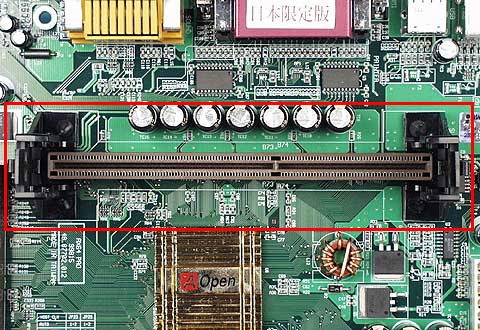
Slot 1
Slot 1
Main page
2195935

Slot 1

logo
Community Hub0 subscribers
Read side by side
from Wikipedia
Slot 1
TypeSlot
Chip form factors
Contacts242[1]
FSB protocolAGTL+
FSB frequency66, 100, and (on third-party chipsets) 133 MHz
Voltage range1.3 to 3.50 V
ProcessorsPentium II: 233–450 MHz

Celeron: 266–433 MHz
Pentium III: 450 MHz–1.13 GHz
(A Slotket makes following Socket 370 CPUs usable:
Celeron and Pentium III to 1,400 MHz,
VIA Cyrix III: 350–733 MHz,
VIA C3: 733–1,200 MHz

Slotkets also made it possible to use some Pentium Pro CPUs for Socket 8 using the same method.)
PredecessorSocket 7
SuccessorSocket 370

This article is part of the CPU socket series
Pentium II SECC form installed into Slot 1

Slot 1 refers to the physical and electrical specification for the connector used by some of Intel's microprocessors, including the Pentium Pro, Celeron, Pentium II and the Pentium III. Both single and dual processor configurations were implemented.

Intel reverted to the traditional socket interface with the release of Socket 370 in 1999.

General

[edit]

With the introduction of the Pentium II CPU, the need for greater access for testing had made the transition from socket to slot necessary. Previously with the Pentium Pro, Intel had combined processor and cache dies in the same Socket 8 package. These were connected by a full-speed bus, resulting in significant performance benefits. Unfortunately, this method required that the two components be bonded together early in the production process, before testing was possible. As a result, a single, tiny flaw in either die made it necessary to discard the entire assembly, causing low production yield and high cost.[citation needed]

Intel subsequently designed a circuit board where the CPU and cache remained closely integrated, but were mounted on a printed circuit board, called a Single-Edged Contact Cartridge (SECC). The CPU and cache could be tested separately, before final assembly into a package, reducing cost and making the CPU more attractive to markets other than that of high-end servers. These cards could also be easily plugged into a Slot 1, thereby eliminating the chance for pins of a typical CPU to be bent or broken when installing in a socket.

A Slot A CPU on the left compared to a Slot 1 CPU (connector rotated by 180 degrees)

The form factor used for Slot 1 was a 5-inch-long, 242-contact edge connector named SC242. To prevent the cartridge from being inserted the wrong way, the slot was keyed to allow installation in only one direction. The SC242 was later used for AMD's Slot A as well, and while the two slots were identical mechanically, they were electrically incompatible. To discourage Slot A users from trying to install a Slot 1 CPU, the connector was rotated 180 degrees on Slot A motherboards. This also allowed motherboard manufacturers to save costs by stocking the same part for both Slot 1 and Slot A assemblies.

With the new Slot 1, Intel added support for symmetric multiprocessing (SMP). A maximum of two Pentium II or Pentium III CPUs can be used in a dual slot motherboard. The Celeron does not have official SMP support.

There are also converter cards, known as Slotkets, which hold a Socket 8 so that a Pentium Pro CPU can be used with Slot 1 motherboards.[2] These specific converters, however, are rare. Another kind of slotket allows using a Socket 370 CPU in a Slot 1. These are generally more common than Socket 8 to Slot 1 slotkets. Many of these latter devices are equipped with their own voltage regulator modules, in order to supply the new CPU with a lower core voltage, which the motherboard would not otherwise allow.

Form factors

[edit]
Intel Pentium II CPU in SECC form factor
Pentium III (Katmai) in SECC2: CPU at center, two chips at right are cache
Celeron in SEPP: CPU at center (under heat spreader), surrounding chips are resistors and bypass capacitors

The Single Edge Contact Cartridge, or "SECC", was used at the beginning of the Slot 1-era for Pentium II CPUs. Inside the cartridge, the CPU itself is enclosed in a hybrid plastic and metal case. The back of the housing is plastic and has several markings on it: the name, "Pentium II"; the Intel logo; a hologram; and the model number. The front consists of a black anodized aluminum plate, which is used to hold the CPU cooler. The SECC form is very solid, because the CPU itself is resting safely inside the case. As compared to socket-based CPUs, there are no pins that can be bent, and the CPU is less likely to be damaged by improper installation of a cooler.

Following SECC, the SEPP-form (Single Edge Processor Package) appeared on the market. It was designed for lower-priced Celeron CPUs. This form lacks a case entirely, consisting solely of the printed-circuit board holding the components.

A form factor called SECC2 was used for late Pentium II and Pentium III CPUs for Slot 1, which was created to accommodate the switch to flip chip packaging.[3] Only the front plate was carried over, the coolers were now mounted straight to the PCB and exposed CPU die and are, as such, incompatible with SECC cartridges.

History

[edit]

Historically, there are three platforms for the Intel P6 CPUs: Socket 8, Slot 1 and Socket 370.

Slot 1 is a successor to Socket 8. While the Socket 8 CPUs (Pentium Pro) directly had the L2-cache embedded into the CPU, it is located (outside of the core) on a circuit board shared with the core itself. The exception is later Slot 1 CPUs with the Coppermine core which have the L2-cache embedded into the die.

In the beginning of 2000, around the time the Coppermine Pentium III CPUs with FC-PGA housing were already commonplace, Slot 1 was being gradually phased out in favor of Socket 370, well after Intel started to offer both Socket 370 and Slot 1 CPUs at the same time since late 1998. Socket 370 was initially made for low-cost Celeron processors starting with the Mendocino Celerons, while Slot 1 was thought of as a platform for the more expensive Pentium II and early Pentium III models. Both cache and core were embedded into the die.

Slot 1 also obsoleted the old Socket 7 as the standard platform for home users, at least regarding Intel. After superseding the Intel P5 Pentium MMX CPU in the late 1990s, Intel had completely left the Socket 7 market.

Chipsets and officially supported CPUs[4][5]

[edit]
Slot 1/Socket 370 Converter
Slot 1/Socket 8 Converter

Intel 440FX [6]

[edit]
  • Introduced in: May 6, 1996
  • FSB: 66 MHz
  • PIO/WDMA
  • Supported RAM type: EDO-DRAM
  • Supported CPUs:
  • Used in both Socket 8 (Pentium Pro) and Slot 1 (Pentium II, early Celerons)
  • Does not support AGP or SDRAM, as it predates the introduction of said technologies
  • Allowed up to two CPUs for SMP

Intel 440LX [7]

[edit]
  • Introduced in: August 27, 1997
  • FSB: 66 MHz
  • Supported RAM type: EDO-DRAM, SDRAM
  • Supported CPUs: Pentium II, Celeron
  • AGP 2× Mode
  • UDMA/33
  • Introduced support for AGP and SDRAM
  • Allowed up to two CPUs for SMP

Intel 440EX [8]

[edit]
  • Introduced in: April, 1998
  • FSB: 66 MHz
  • Supported RAM type: EDO-DRAM, SDRAM
  • Supported CPUs: Pentium II, Celeron
  • AGP 2× Mode
  • UDMA/33
  • Same specifications as 440LX, but memory support limited to 256 MB and no SMP support.

Intel 440BX [9]

[edit]
  • Introduced in: April 1998
  • FSB: 66 and 100 MHz (some motherboards supported overclocking to 133 MHz, allowing usage of Socket 370 CPUs using a Slocket)
  • AGP 2× Mode (max aperture size 32 or 64 MB)
  • UDMA/33
  • Supported RAM types: SDRAM (PC66 and PC100, PC133 with overclocking) up to 4 DIMMs of 256 MB
  • Supported CPUs:
  • Allowed up to two CPUs for SMP

Intel 440ZX

[edit]
  • Introduced in: November 1998
  • FSB: 66 and 100 MHz (some motherboards supported overclocking to 133 MHz, allowing usage of Socket 370 CPUs using a Slocket)
  • AGP 2× Mode
  • UDMA/33
  • Supported RAM types: SDRAM (PC66 and PC100, PC133 with overclocking), up to 2 DIMMs of 256 MB
  • Supported CPUs:

Intel 810

[edit]
  • Introduced in: 1999
  • FSB: 66 and 100 MHz
  • No external AGP
  • Intel i752 based graphics
  • UDMA/66 (UDMA/33 with ICH0)
  • Supported RAM types: PC100 SDRAM
  • Supported CPUs:

Intel 820/820E (Camino)

[edit]
  • Introduced in: November 1999
  • FSB: 100 and 133 MHz
  • AGP 4× Mode
  • UDMA/66 (i820), UDMA/100 (i820E)
  • Supported RAM types: RDRAM, SDRAM (PC100 via MTH)
  • Supported CPUs: All FSB 100/133 Slot 1 CPUs
  • Allowed up to two CPUs for SMP

Intel 840

[edit]
  • Introduced in: November 1999
  • FSB: 100 and 133 MHz
  • AGP 4× Mode
  • UDMA/66 (i820), UDMA/100 (i820E)
  • Supported RAM types: Dual Channel RDRAM, SDRAM (PC100 via MTH)
  • Supported CPUs: All FSB 100/133 Slot 1 CPUs
  • Allowed up to two CPUs for SMP

VIA Apollo Pro / Pro II / Pro+

[edit]
  • Introduced in: May 1998 (Pro Plus: Dec 1998)
  • FSB: 66, 100 MHz (some motherboards supported overclocking to 133 MHz, allowing usage of Socket 370 CPUs using a Slocket)
  • AGP 2× Mode
  • UDMA/33 (VT82C586B/VT82C596A), UDMA/66 (VT82C596B)
  • Supported RAM types: PC66/100 SDRAM up to 1536 MB
  • Supported CPUs:

VIA Apollo Pro 133

[edit]
  • Introduced in: July 1999
  • FSB: 66, 100, and 133 MHz
  • AGP 2× Mode
  • UDMA/33 (VT82C596A), UDMA/66 (VT82C596B/VT82C686A), UDMA/100 (VT82C686B)
  • Supported RAM types: PC66/100/133 SDRAM up to 1536 MB
  • Supported CPUs: All Slot 1 CPUs

VIA Apollo Pro 133A

[edit]
  • Introduced in: Oct 1999
  • FSB: 66, 100, and 133 MHz
  • AGP 4× Mode
  • UDMA/66 (VT82C596B/VT82C686A), UDMA/100 (VT82C686B)
  • Supported RAM types: PC66/100/133 SDRAM up to 2048 MB
  • Supported CPUs: All Slot 1 CPUs
  • Allowed up to two CPUs for SMP

SiS 5600 (SiS 600)

[edit]
  • Introduced in: November 1998
  • FSB: 66 and 100 MHz
  • AGP 2× Mode
  • UDMA/33
  • Supported RAM types: PC66/100 SDRAM up to 1536 MB
  • Supported CPUs:

SiS 620

[edit]
  • Introduced in: April 1999
  • FSB: 66 and 100 MHz
  • No external AGP port
  • SiS 6326 based Integrated Graphics
  • UDMA/33
  • Supported RAM types: PC66/100 SDRAM up to 1536 MB
  • Supported CPUs:

See also

[edit]

References

[edit]
[edit]
Revisions and contributorsEdit on WikipediaRead on Wikipedia
from Grokipedia
Slot 1 is a proprietary 242-pin edge connector (SC242) developed by Intel as the primary interface for its Pentium II and early Pentium III microprocessors, which were housed in Single Edge Contact Cartridge (SECC) or Single Edge Processor Package (SEPP) formats to integrate the CPU die, L2 cache, and thermal solutions into a removable module.[1][2] Introduced on May 7, 1997, alongside the launch of the Pentium II processor at speeds starting from 233 MHz, Slot 1 marked a shift from traditional pin-grid array sockets to a cartridge-based design aimed at simplifying upgrades and enhancing thermal management for desktop and workstation systems.[3] The Slot 1 architecture supported a 64-bit data bus and front-side bus (FSB) speeds of 66 MHz and 100 MHz, enabling efficient communication between the processor and the motherboard chipset while utilizing Gunning Transceiver Logic+ (GTL+) signaling for reduced power consumption and noise.[2] It was compatible with several Intel chipsets, including the 440FX (Natoma), 440LX (Natoma), 440EX (Balboa), and notably the 440BX (Seattle), which became the most popular due to its support for 100 MHz FSB, AGP graphics, and up to 1 GB of SDRAM. Processors using Slot 1 featured the P6 microarchitecture, with integrated MMX instructions in Pentium II models and the addition of Streaming SIMD Extensions (SSE) in Pentium III variants, alongside 256 KB or 512 KB of on-cartridge L2 cache running at full core speed.[2] Over its lifespan from 1997 to approximately 2001, Slot 1 powered a range of processors including the Pentium II (Klamath and Deschutes cores at 233–450 MHz), low-end Celeron variants (Deschutes core at 300–533 MHz), and Pentium III models (Katmai and Coppermine cores up to 1 GHz), achieving clock speeds that pushed the limits of the 0.35 μm to 0.18 μm fabrication processes. The design emphasized modularity, with thermal specifications requiring heatsinks to maintain case temperatures below 70–75°C under power dissipation of 20–30 W.[1] However, its larger form factor and higher cost compared to pin-based sockets led Intel to phase it out in favor of Socket 370 (PGA370) for later Pentium III and Celeron processors starting in 1999, culminating in the full transition to Socket 423 with the Pentium 4 in 2000.[4]

Overview

Definition and purpose

Slot 1 is a proprietary CPU connector standard developed by Intel, introduced in 1997 as an edge connector interface for its Pentium II and Pentium III processors, utilizing a 242-contact slot known as SC 242.[1][2] This slot-based design marked a departure from the traditional pin grid array (PGA) sockets used in prior generations, such as Socket 7, by employing a removable cartridge that housed the processor die, L2 cache chips, and passive components on a printed circuit board substrate.[1] The architecture facilitated easier installation and removal compared to soldered or ZIF PGA solutions, while providing mechanical stability and protection for sensitive internals.[1] The primary purpose of Slot 1 was to enable higher performance in computing systems by supporting system bus speeds ranging from 66 MHz to 133 MHz, which exceeded the capabilities of Socket 7's typical 66 MHz limit and allowed for improved data throughput between the CPU, memory, and I/O subsystems.[5][2] It incorporated an integrated L2 cache within the Single Edge Contact Cartridge (SECC or SECC2) packaging, typically 256 KB or 512 KB in size, running at full or half core speed to enhance memory access efficiency without relying on motherboard-mounted cache.[5][1] Additionally, the cartridge design improved heat dissipation through an integrated thermal plate or direct heatsink attachment points, addressing the thermal challenges of higher clock speeds and power dissipation in multi-transistor dies.[2][5] Initially targeted at consumer desktops, workstations, and entry-level servers, Slot 1 provided scalability beyond Socket 7 by accommodating the evolving demands of multimedia, scientific computing, and business applications in the late 1990s.[2][5] This interface supported binary compatibility with earlier Intel Architecture processors while introducing features like the GTL+ bus protocol for robust signaling at elevated frequencies.[2] The SECC form factor, resembling a scaled-down PCI expansion card, simplified upgrades and contributed to the platform's adoption in OEM systems requiring reliable high-volume production.[1]

Key specifications

Slot 1 utilizes a 242-pin edge connector for interfacing the processor cartridge with the motherboard.[6] This connector supports electrical signaling primarily through GTL+ protocol, with termination voltage (VTT) at 1.5 V ± 9% (ranging from 1.365 V to 1.635 V) and reference voltage (VREF) at two-thirds of VTT.[6] Additionally, certain I/O signals, such as those for the L2 cache (VCCL2), operate at 3.3 V to ensure compatibility with system components.[2] The front-side bus (FSB) frequencies supported include 66 MHz, 100 MHz, and 133 MHz, determined by the processor model and chipset configuration.[7] Mechanically, the Slot 1 connector measures approximately 5.255 inches (13.35 cm) in length for the single-edge contact (SEC) cartridge interface, enabling secure insertion and extraction up to 50 cycles.[2] The edge fingers feature gold-plated contacts to minimize resistance and ensure reliable electrical connectivity over time.[6] Supported processors draw a maximum power of up to 30 W under typical operating conditions, with variations based on clock speed and thermal design (e.g., 27.1 W for 450 MHz Pentium II models).[2] The protocol employed is GTL+ (Gunning Transceiver Logic+), an open-drain signaling scheme with external pull-up resistors to VTT, designed to reduce electromagnetic interference and ringing while enabling higher bus speeds.[6] GTL+ provides larger noise margins compared to earlier GTL implementations, with edge rates specified between 0.3 V/ns and 0.8 V/ns for optimal signal integrity.[6] This protocol applies to key bus signals such as address (A[35:3]#), data (D[63:0]#), and request lines (REQ[4:0]#), all synchronized to the BCLK clock.[6]

Physical design

Connector architecture

The Slot 1 connector, designated as the SC242, features a 242-pin edge connector design with a 1.0 mm pitch, facilitating high-volume desktop systems integration with Single Edge Contact Cartridge (SECC) processors.[1] This structure includes keyed notches along the edge for alignment, ensuring unidirectional insertion to prevent misalignment or damage during installation.[8] Electrically, the connector allocates specific pins for core functions, including multiple dedicated VCC pins for power distribution—such as VCC_CORE at 2.0 V for the processor core, VCC_L2 at 3.3 V for L2 cache support, and VCC_VTT at 1.5 V for AGTL+ bus termination—alongside VCC5 at 5 V. Ground (VSS) pins, numbering around 30, are distributed to minimize inductance and support signal integrity. Address and data lines, comprising 141 AGTL+ bus signals, occupy dedicated pins for bidirectional communication, while control signals include BSEL[1:0] pins for selecting system bus frequencies (66 MHz, 100 MHz, or 133 MHz).[8] To maintain stability given the cartridge's weight, the connector integrates with a retention mechanism typically consisting of plastic clips or brackets mounted on the motherboard, which cradle and secure the SECC against vibration and thermal expansion.[9]

Cartridge form factor

The Single Edge Contact Cartridge (SECC) served as the primary packaging form factor for Slot 1 processors, consisting of a plastic enclosure that houses the CPU die, L2 cache chips, and associated components on a printed circuit board substrate. The substrate features an edge finger connector with 242 contacts at a 1.0 mm pitch, designed for insertion into the Slot 1 motherboard slot. Inside the cartridge, the CPU die is mounted alongside surface-mount L2 cache chips, typically providing up to 512 KB of integrated cache memory using TagRAM and Burst Static RAM (BSRAM) modules. An aluminum thermal plate, coated in black anodization for improved heat dissipation, is attached to the CPU die via a thermal interface material and secured with clips, facilitating effective heat sinking.[1][10] A variant known as SECC2 was introduced to enhance thermal performance by eliminating the extended thermal plate, allowing direct attachment of a heatsink to the processor core through the cartridge cover, which reduces thermal resistance. This design incorporated an integrated heat spreader on the CPU for better heat distribution and compatibility with higher-performance cooling solutions. The overall dimensions of the SECC and SECC2 cartridges measure approximately 12.7 cm in length, 6.2 cm in width, and 1.25 cm in height, providing a compact yet robust module for desktop and workstation applications.[10] Key advantages of the SECC form factor include protection of the electrical contacts, as the edge finger design avoids exposed pins that could be damaged during handling, unlike traditional pin-grid array packages. Additionally, the cartridge includes VID pins that signal the motherboard's VRM to provide the appropriate core voltage, such as 1.9–2.1 V, ensuring compliance with power state transitions and simplifying motherboard design by standardizing voltage regulation on the system board. The cartridge's edge connector ensures pin compatibility with the Slot 1 interface.[10][1]

Historical context

Development origins

In the mid-1990s, Intel's research and development initiatives sought to address the constraints of the Socket 7 interface, which supported Pentium processors but limited front-side bus (FSB) speeds to 66 MHz and hindered scalability for higher-performance designs. This effort targeted successor CPU projects internally code-named Klamath and Deschutes, leading to the conceptualization of Slot 1 as a new connector to enable faster bus operations and modular packaging.[11][12] A primary engineering driver for Slot 1 was the requirement for an off-die L2 cache, which allowed Intel to deliver substantial performance gains—such as reduced latency and higher bandwidth—without enlarging the CPU die and thereby escalating production costs associated with on-chip integration. This strategy drew inspiration from the earlier Socket 8 design for the Pentium Pro, where cache was implemented in a multi-chip module adjacent to the core, but Slot 1 extended the concept by mounting the L2 cache (typically 512 KB synchronous SRAM) on a removable cartridge's printed circuit board for easier assembly and consumer-oriented affordability.[13] Development of Slot 1 was spearheaded by Intel's Architecture Labs, the company's central R&D division responsible for advancing PC architectures during the 1990s, with internal lab testing commencing around 1996 to verify compatibility with emerging 100 MHz FSB capabilities that would become standard in later implementations.[14][15]

Timeline of releases

Slot 1 was introduced on May 7, 1997, alongside the Klamath-core Pentium II processors operating at clock speeds of 233 MHz, 266 MHz, and 300 MHz.[3][16] This debut marked the first use of the Slot 1 connector for consumer desktop systems, building on the Pentium Pro's Slot 2 architecture but optimized for broader market adoption. In 1998, Slot 1 support expanded with the Deschutes-core Pentium II processors, debuting on January 26 at 333 MHz and scaling up to 450 MHz by August.[17][18] The following year, 1999 saw the introduction of the Katmai-core Pentium III on February 26, starting at 450 MHz and reaching 600 MHz by September, enhancing multimedia capabilities through the addition of SSE instructions while maintaining compatibility with existing Slot 1 motherboards.[19] By 2000 and 2001, Slot 1 accommodated the Coppermine-core Pentium III, released on October 25, 1999, with speeds from 500 MHz to 1 GHz. However, Intel began phasing out Slot 1 in favor of the more compact Socket 370 interface around 2000, with full discontinuation of new Slot 1 processor production by 2002 as Coppermine and later cores transitioned to socket designs.[20][4]

Supported processors

Pentium II processors

The Pentium II processors, introduced by Intel in May 1997, represented the inaugural CPU family engineered specifically for the Slot 1 interface, building on the P6 microarchitecture from the Pentium Pro while integrating MMX instructions for enhanced multimedia processing. These processors were housed in a Single Edge Contact Cartridge (SECC) form factor, which encapsulated the CPU die, heat sink, and 512 KB of off-die L2 cache to improve thermal management and system integration. With approximately 7.5 million transistors, the Pentium II family delivered higher overall performance than its predecessors, maintaining binary compatibility with earlier Intel x86 processors.[16][21] The Klamath core, the first iteration of the Pentium II, was fabricated using a 0.35 μm CMOS process and launched at clock speeds of 233 MHz, 266 MHz, and 300 MHz. It operated on a 66 MHz front-side bus (FSB) with GTL+ signaling, and its 512 KB L2 cache ran at half the core clock speed (116.5 MHz for the 233 MHz model), providing unified, non-blocking access to support dynamic execution features like out-of-order processing and branch prediction. Klamath processors consumed up to 25 watts of power at a core voltage of 2.8 V, targeting desktop and entry-level workstation applications.[12][21] Succeeding Klamath, the Deschutes core debuted in early 1998 on a more efficient 0.25 μm process, enabling higher clock speeds ranging from 266 MHz to 450 MHz while reducing power draw to around 24 watts at similar voltages. Early Deschutes models retained the 66 MHz FSB, but later variants supported 100 MHz FSB for increased bandwidth, aligning with the Slot 1's design capabilities. A major refinement was the full-speed L2 cache option, operating at the core frequency to minimize latency and boost throughput in cache-sensitive workloads, all while retaining MMX instruction set compatibility.[22][2][23] Overall, the Pentium II processors achieved significant performance uplifts over the Socket 7-based Pentium MMX, with the integrated 512 KB L2 cache and higher FSB contributing to faster data access and execution; for instance, in CPU Mark 32 benchmarks, a 233 MHz Klamath scored 605 points compared to 464 for a 225 MHz Pentium MMX. These gains were particularly evident in floating-point and multimedia tasks leveraging MMX, where the P6 architecture's superscalar design provided up to 30-50% better efficiency per clock cycle in select applications.[16]

Pentium III processors

The Pentium III processors represented the final major evolution of Intel's Slot 1-compatible CPUs, building on the P6 microarchitecture with enhancements in instruction sets and cache design to improve multimedia and computational performance. These processors were packaged in Single Edge Contact Cartridge 2 (SECC2) form factors for Slot 1, maintaining compatibility with existing motherboards while introducing features like processor serial numbers for security and identification. Slot 1 support for Pentium III spanned from 1999 to 2001, after which Intel phased out the cartridge in favor of pin-grid array sockets. The Katmai core, launched in February 1999, marked the debut of the Pentium III lineup for Slot 1, with clock speeds ranging from 450 MHz to 600 MHz fabricated on a 250 nm process. It featured 9.5 million transistors in the core, plus an additional 25 million for the off-die 512 KB L2 cache operating at half the processor speed, and a 16 KB L1 instruction cache alongside a 16 KB L1 data cache. A key innovation was the introduction of 70 Streaming SIMD Extensions (SSE) instructions, enabling accelerated vector processing for floating-point operations in applications like 3D graphics and scientific simulations. These processors dissipated up to 28 W of thermal design power (TDP) and used a 100 MHz front-side bus, providing an 11% frequency uplift over the highest-speed Pentium II equivalents. Succeeding Katmai, the Coppermine core arrived in October 1999, shifting to a 180 nm process with 28 million transistors and integrating 256 KB of full-speed on-die L2 cache—reducing latency and eliminating the need for external cache chips in the cartridge. Clock speeds for Slot 1 variants extended from 500 MHz to a peak of 1.13 GHz, supporting both 100 MHz and 133 MHz bus options in later models, with TDP ranging from 21.5 W to 31.1 W depending on frequency. This design improved overall efficiency and bandwidth, particularly for cache-intensive workloads, while retaining SSE support and adding optimizations like advanced transfer cache for better prefetching. The Tualatin core, introduced in 2001, refined the architecture further on a 130 nm process with 47 million transistors, 512 KB of on-die L2 cache at full speed, and improved power management for lower voltage operation (1.475 V core), achieving speeds from 1.13 GHz to 1.4 GHz with TDPs as low as 27.7 W. Although officially designed for Socket 370, third-party adapters like the PowerLeap Slotket III enabled unofficial Slot 1 compatibility on select motherboards with BIOS updates and voltage adjustments, extending the platform's lifespan for enthusiasts. Tualatin's enhancements focused on branch prediction and pipeline efficiency, yielding up to 20% better performance per clock over Coppermine in integer tasks. Official Slot 1 Pentium III production concluded in 2001 with the 1.13 GHz Coppermine model, as Intel redirected development toward Socket 370 and emerging NetBurst architectures, signaling the end of cartridge-based designs.

Celeron processors

Slot 1 also supported low-end Celeron processors, introduced in April 1998 as a cost-reduced alternative to the Pentium II, using the same P6 microarchitecture but with reduced features like smaller or no L2 cache to lower price. These were aimed at budget desktop systems and initially packaged in SECC form factors for Slot 1 compatibility. The Covington core Celeron, based on the Deschutes design but without L2 cache, launched at 266 MHz and 300 MHz on a 0.25 μm process, operating at 66 MHz FSB with power consumption around 17 W at 2.0 V. This no-cache design led to performance penalties in cache-dependent tasks but offered good value for basic computing. Succeeding Covington, the Mendocino core debuted in August 1999 on a 0.18 μm process with 19 million transistors and 128 KB of on-die full-speed L2 cache, significantly improving performance over Covington. Slot 1 variants ranged from 333 MHz to 533 MHz, supporting 66 MHz and 100 MHz FSB options, with TDP up to 20 W. The integrated cache and smaller die size enhanced efficiency, making Mendocino Celerons popular for upgrades on existing Slot 1 motherboards until the transition to Socket 370 in late 1999.[24]

Compatible chipsets

Intel chipsets

Intel's chipsets for the Slot 1 platform formed the backbone of early Pentium II and Pentium III systems, providing official support for the cartridge-based processors through integrated northbridge and southbridge components optimized for performance and compatibility. These chipsets evolved to address increasing demands for faster front-side bus (FSB) speeds, advanced graphics interfaces, and memory technologies, while maintaining Intel's proprietary architecture for validated stability. The lineup began with basic PCI-centric designs and progressed to support for AGP and emerging DRAM types, though some later iterations faced challenges with cost and reliability. The 440FX, codenamed Natoma and released in 1997, was the inaugural chipset for Slot 1, supporting a 66 MHz FSB and up to 1 GB of EDO DRAM across four 72-pin SIMM slots. It featured the 82441FX PCI and memory controller without AGP support, relying instead on PCI slots for graphics expansion, and paired with the PIIX3 southbridge for IDE and USB 1.1 connectivity. Designed initially for Pentium Pro but adapted for early Pentium II processors, it emphasized robust system addressing up to 4 GB while ensuring backward compatibility with prior Intel architectures. Succeeding it, the 440LX chipset, introduced in 1998 and codenamed Balboa, advanced to a 100 MHz FSB for improved processor bandwidth, alongside AGP 2x support and PC100 SDRAM compatibility for up to 1 GB of memory. This chipset's 82443LX northbridge enabled better graphics performance through the Accelerated Graphics Port and synchronous DRAM, marking a shift toward mainstream desktop acceleration while supporting Slot 1 Pentium II CPUs up to 450 MHz. Its architecture balanced cost and features, becoming a staple in mid-range systems. The 440BX, launched later in 1998, emerged as the most enduring and popular Slot 1 chipset due to its support for 100/133 MHz FSB, AGP 4x, and up to 1 GB of PC133 SDRAM, paired with the PIIX4E southbridge for enhanced ATA/66 storage. Known for exceptional overclocking stability—allowing reliable operation beyond official speeds on compatible motherboards—it powered high-performance builds with Pentium III processors and remained viable into the early 2000s. The 82443BX northbridge optimized data throughput, contributing to its widespread adoption in gaming and workstation platforms. As a more affordable derivative, the 440ZX chipset arrived in 1999, functioning as a budget-oriented variant of the 440BX with 66/100 MHz FSB support, AGP 2x, and up to 1 GB of PC100 SDRAM. It introduced options for integrated graphics via compatible southbridges like the PIIX4E, targeting entry-level systems while retaining core Slot 1 compatibility for Pentium II and III processors. Though less capable than its predecessor in peak performance, it offered cost savings without sacrificing essential connectivity. The i810 chipset, released in 1999 and aimed at low-end consumer systems, integrated 3D graphics acceleration via the i752 core, supporting 66/100 MHz FSB and up to 512 MB of PC100 SDRAM without an external AGP slot. Designed for value-oriented Slot 1 builds with Pentium II or Celeron processors, it included the 82810 GMCH northbridge and ICH0 southbridge for UDMA/33 IDE, emphasizing all-in-one functionality to reduce component costs in home PCs. Later, the 820 and 820E chipsets, codenamed Camino and introduced in late 1999, shifted to Rambus Direct RDRAM (Direct RDRAM) for memory, supporting 100/133 MHz FSB, AGP 4x, and up to 1 GB of RDRAM in a 4-channel configuration, with the 820E adding ATA/100 support. However, these were hampered by high RDRAM module costs—often exceeding the processor price—and instability issues like signal integrity problems at high speeds, leading to limited adoption despite Slot 1 compatibility for Pentium III CPUs. The 82820M northbridge aimed for bandwidth gains but faced criticism for real-world performance shortfalls. Finally, the 840 chipset, released in 2000 as an extension of the 820 architecture and codenamed Carmel, enhanced RDRAM handling with dual-channel PC800 support for up to 2 GB, 100/133 MHz FSB, and AGP 4x, specifically enabling dual-processor Slot 1 configurations in workstation environments. It addressed some 820 shortcomings through improved memory interleaving and 64-bit PCI support via the 82840 MCH, though RDRAM expenses continued to hinder broader use. This chipset targeted professional applications with Pentium III Xeon processors, providing scalable bandwidth for multi-threaded workloads.

VIA chipsets

VIA Technologies entered the Slot 1 chipset market in 1998 with the Apollo Pro, offering a cost-effective alternative to Intel's 440FX and 440BX chipsets by supporting both 66 MHz and 100 MHz front-side bus (FSB) speeds, AGP 2x interface, and SDRAM memory up to 1 GB with ECC support. This two-chip design, consisting of the VT82C691 Northbridge and VT82C596 Southbridge, ensured compatibility with Pentium II and Celeron processors while incorporating innovations like SideBand Addressing for improved AGP performance and asynchronous memory timing to pair 100 MHz FSB CPUs with 66 MHz SDRAM. Released in May 1998, the Apollo Pro quickly gained traction among motherboard manufacturers for its balanced feature set, enabling mainstream Slot 1 systems without the premium pricing of Intel solutions.[25] Building on this foundation, VIA introduced the Apollo Pro 133 in July 1999, extending FSB support to 133 MHz to accommodate emerging Pentium III processors and incorporating ATA/66 for faster hard drive performance.[26] The chipset, featuring the VT82C693A Northbridge, maintained SDRAM compatibility (PC100/PC133 up to 1.5 GB) and AGP 2x, positioning it as an accessible upgrade path for users transitioning from Pentium II systems. Priced at $29 in OEM quantities, it targeted value-conscious builders seeking performance parity with Intel's 440BX at a lower cost, though it required careful BIOS tuning for stability at higher FSB speeds.[26] The Apollo Pro 133A, launched in October 1999, refined the lineup with AGP 4x support for enhanced graphics bandwidth and improved voltage regulation to better handle Coppermine-core Pentium III CPUs, including those with 133 MHz FSB.[27] Using the VT82C694X Northbridge paired with the VT82C686A/B Southbridge, it added ATA/100 in later revisions and supported up to 1.5 GB of PC133 SDRAM, making it a versatile choice for mid-range Slot 1 builds through 2000.[28] This iteration solidified VIA's role in the market by addressing Coppermine-specific power delivery challenges, allowing broader adoption in consumer motherboards without compromising on peripheral integration. In parallel, VIA offered value-oriented variants like the Apollo Pro II and Pro+ in late 1998 and December 1998, respectively, emphasizing 100 MHz FSB support and features such as integrated audio codecs on compatible boards to reduce costs for entry-level Slot 1 systems. These models, based on the VT82C692X Northbridge, retained core Apollo Pro capabilities like AGP 2x and SDRAM support while enabling overclocking to 133 MHz on select motherboards, appealing to budget users upgrading from older platforms.[29] Overall, VIA's Slot 1 chipsets played a key role in democratizing access to Pentium II/III performance, powering numerous third-party motherboards and fostering competition that drove down system prices.

SiS chipsets

Silicon Integrated Systems (SiS) developed chipsets for Slot 1 motherboards that emphasized cost-effectiveness and integration, appealing primarily to original equipment manufacturers (OEMs) seeking budget-friendly platforms for Pentium II and compatible processors. These chipsets provided essential features like AGP support and memory compatibility while prioritizing affordability over high-end performance. The SiS 620 chipset, introduced in 1999, supported Slot 1 Pentium II processors with 66/100 MHz front-side bus (FSB) speeds, AGP 2x mode, and up to 1.5 GB of PC66/100 SDRAM across three DIMM slots, making it a popular entry-level choice for OEMs aiming to reduce system costs. It featured an integrated 3D graphics accelerator based on the SiS 6326 core, enabling basic multimedia capabilities without requiring a separate graphics card, and was priced at approximately $29 in volume for manufacturers. Paired typically with the SiS 5595 southbridge, it included UDMA/33 support for IDE storage, further enhancing its suitability for low-end consumer PCs. The SiS 5600 chipset (also known as SiS 600), launched in late 1998 and available through 2000, extended Slot 1 compatibility with up to 100 MHz FSB support, AGP 2x, and up to 1.5 GB of SDRAM/EDO memory, targeting low-cost systems for home and office use. It incorporated the AGP 6326 integrated graphics engine for 3D acceleration and shared PCI bandwidth, alongside UDMA/33 IDE interfaces via its companion southbridge, allowing OEMs to build economical configurations with onboard video. While BIOS options permitted some FSB adjustments, the chipset's design focused on standard speeds rather than aggressive tuning. SiS chipsets for Slot 1 exhibited limitations in stability during high overclocks compared to Intel counterparts like the 440BX, often showing memory incompatibility issues—such as instability with certain 8ns or 256 MB modules at 100 MHz FSB—and reduced overall bandwidth (10-30% lower in benchmarks), which restricted their appeal in enthusiast builds. These traits stemmed from their emphasis on integration and low pricing, contributing briefly to the third-party ecosystem alongside options like VIA.

Transition and legacy

Shift to socket-based designs

The transition from Slot 1 to socket-based designs for Intel processors began in late 1999, primarily driven by the introduction of the Coppermine-core Pentium III, which integrated the L2 cache directly onto the processor die, eliminating the need for the external Single Edge Processor (SEP) cartridge used in Slot 1 configurations. This shift allowed for the adoption of the Flip-Chip Pin Grid Array (FC-PGA) packaging on the PGA370 socket (also known as Socket 370), which replaced the larger SC242 Slot 1 connector.[7] The Coppermine processors, launched in FC-PGA form for Socket 370, supported clock speeds from 500 MHz to 1.13 GHz and were designed for high-performance desktops, workstations, and servers, offering improved power dissipation through an Integrated Heat Spreader (IHS).[7] To accommodate the large installed base of Slot 1 motherboards, Intel continued producing Coppermine Pentium III variants in the Slot 1 package alongside the new socket versions, while third-party adapters—known as "slockets"—enabled Socket 370 CPUs to be used on existing Slot 1 boards by converting the form factor and providing pin mapping, with voltage regulation provided by the motherboard. These adapters facilitated a smoother migration, allowing users to upgrade without full motherboard replacement. Socket 370 offered several advantages over Slot 1, including lower manufacturing costs, a smaller physical footprint on motherboards, and simpler production processes due to the standardized 370-pin Zero Insertion Force (ZIF) design shared with Celeron processors.[7] Additionally, it supported a 100 MHz or 133 MHz system bus and easier thermal management, making it more suitable for compact systems like laptops where Slot 1 was impractical.[30] The socket design extended to later revisions, supporting the Tualatin-core Pentium III up to 1.4 GHz with 512 KB L2 cache, marking the upper limit for Socket 370 compatibility. As part of Intel's broader strategy, Slot 1 was phased out by 2002 in favor of PGA standardization, aligning with the Pentium 4 launch on Socket 423 in November 2000 and its transition to Socket 478 in 2001 for Northwood cores, which emphasized higher clock speeds and a new NetBurst architecture. This move streamlined production and reduced complexity across Intel's desktop lineup.

Modern relevance

In the contemporary landscape of computing as of 2025, Slot 1 maintains niche significance through retro computing enthusiasts who value its role in authentic reproduction of late-1990s PC experiences. The broader surge in retro gaming, driven by nostalgia and accessibility via online platforms, has spotlighted Slot 1 systems for running original DOS and Windows 98 software on period-correct hardware.[31][32] This legacy use often involves modifications for compatibility with current infrastructure, such as adapters enabling modern ATX power supplies to power Slot 1 motherboards originally designed for AT form factors.[33] Among collectors, Slot 1 processors command notable value, particularly rare variants like the 450 MHz Deschutes-core Pentium II, with eBay sales as of 2025 typically ranging from $10 to $50 USD depending on condition and provenance.[34][35] Open-source firmware initiatives have extended Slot 1's viability; for instance, Coreboot provides ongoing support for compatible motherboards like the ASUS P3B-F, allowing firmware customization and revival of these systems without proprietary BIOS dependencies.[36] As Slot 1 hardware becomes obsolete following the industry's shift to socket-based designs in the early 2000s, discarded systems contribute to global e-waste streams, posing environmental and health risks through improper disposal of hazardous materials like heavy metals and plastics.[37]

References

User Avatar
No comments yet.