Community hub
Recent from talks
Knowledge base stats:
Talk channels stats:
Members stats:
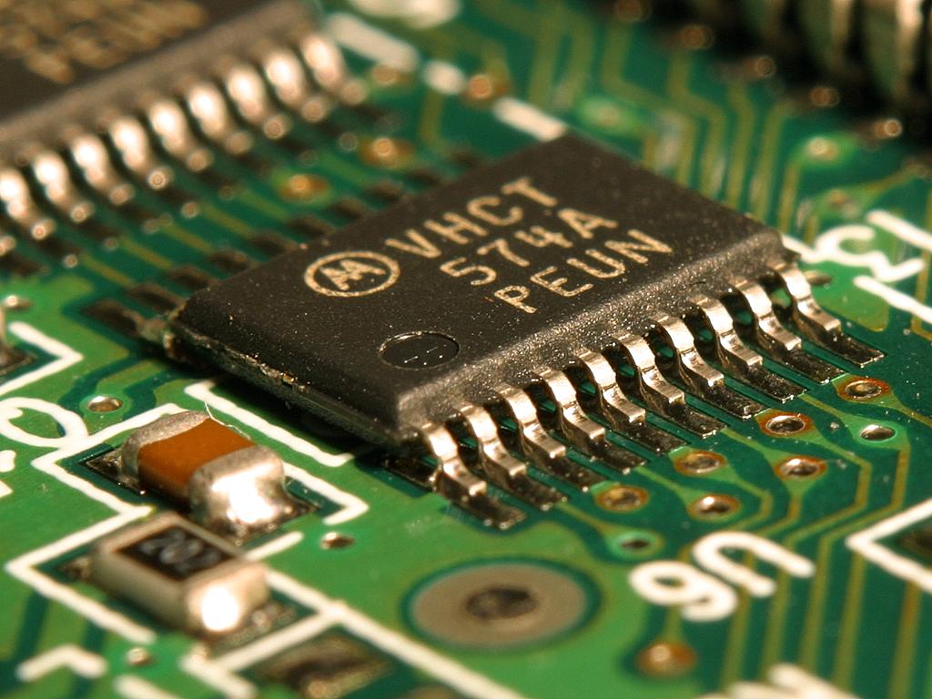
Solid-state electronics
Solid-state electronics are semiconductor electronics: electronic equipment that use semiconductor devices such as transistors, diodes and integrated circuits (ICs). The term is also used as an adjective for devices in which semiconductor electronics that have no moving parts replace devices with moving parts, such as the solid-state relay, in which transistor switches are used in place of a moving-arm electromechanical relay, or the solid-state drive (SSD), a type of semiconductor memory used in computers to replace hard disk drives, which store data on a rotating disk.
The term solid-state became popular at the beginning of the semiconductor era in the 1960s to distinguish this new technology. A semiconductor device works by controlling an electric current consisting of electrons or holes moving within a solid crystalline piece of semiconducting material such as silicon, while the thermionic vacuum tubes it replaced worked by controlling a current of electrons or ions in a vacuum within a sealed tube.
Although the first solid-state electronic device was the cat's whisker detector, a crude semiconductor diode invented around 1904, solid-state electronics started with the invention of the transistor in 1947. Before that, all electronic equipment used vacuum tubes, because vacuum tubes were the only electronic components that could amplify—an essential capability in all electronics. The transistor, which was invented by John Bardeen and Walter Houser Brattain while working under William Shockley at Bell Laboratories in 1947, could also amplify, and replaced vacuum tubes. The first transistor hi-fi system was developed by engineers at GE and demonstrated at the University of Philadelphia in 1955. In terms of commercial production, The Fisher TR-1 was the first "all transistor" preamplifier, which became available mid-1956. In 1961, a company named Transis-tronics released a solid-state amplifier, the TEC S-15.
The replacement of bulky, fragile, energy-hungry vacuum tubes by transistors in the 1960s and 1970s created a revolution not just in technology but in people's habits, making possible the first truly portable consumer electronics such as the transistor radio, cassette tape player, walkie-talkie and quartz watch, as well as the first practical computers and mobile phones. Other examples of solid state electronic devices are the microprocessor chip, LED lamp, solar cell, charge coupled device (CCD) image sensor used in cameras, and semiconductor laser.
Also during the 1960s and 1970s, television set manufacturers switched from vacuum tubes to semiconductors, and advertised sets as "100% solid state" even though the cathode-ray tube (CRT) was still a vacuum tube. It meant only the chassis was 100% solid-state, not including the CRT. Early advertisements spelled out this distinction, but later advertisements assumed the audience had already been educated about it and shortened it to just "100% solid state". LED displays can be said to be truly 100% solid-state.
Hub AI
Solid-state electronics AI simulator
(@Solid-state electronics_simulator)
Solid-state electronics
Solid-state electronics are semiconductor electronics: electronic equipment that use semiconductor devices such as transistors, diodes and integrated circuits (ICs). The term is also used as an adjective for devices in which semiconductor electronics that have no moving parts replace devices with moving parts, such as the solid-state relay, in which transistor switches are used in place of a moving-arm electromechanical relay, or the solid-state drive (SSD), a type of semiconductor memory used in computers to replace hard disk drives, which store data on a rotating disk.
The term solid-state became popular at the beginning of the semiconductor era in the 1960s to distinguish this new technology. A semiconductor device works by controlling an electric current consisting of electrons or holes moving within a solid crystalline piece of semiconducting material such as silicon, while the thermionic vacuum tubes it replaced worked by controlling a current of electrons or ions in a vacuum within a sealed tube.
Although the first solid-state electronic device was the cat's whisker detector, a crude semiconductor diode invented around 1904, solid-state electronics started with the invention of the transistor in 1947. Before that, all electronic equipment used vacuum tubes, because vacuum tubes were the only electronic components that could amplify—an essential capability in all electronics. The transistor, which was invented by John Bardeen and Walter Houser Brattain while working under William Shockley at Bell Laboratories in 1947, could also amplify, and replaced vacuum tubes. The first transistor hi-fi system was developed by engineers at GE and demonstrated at the University of Philadelphia in 1955. In terms of commercial production, The Fisher TR-1 was the first "all transistor" preamplifier, which became available mid-1956. In 1961, a company named Transis-tronics released a solid-state amplifier, the TEC S-15.
The replacement of bulky, fragile, energy-hungry vacuum tubes by transistors in the 1960s and 1970s created a revolution not just in technology but in people's habits, making possible the first truly portable consumer electronics such as the transistor radio, cassette tape player, walkie-talkie and quartz watch, as well as the first practical computers and mobile phones. Other examples of solid state electronic devices are the microprocessor chip, LED lamp, solar cell, charge coupled device (CCD) image sensor used in cameras, and semiconductor laser.
Also during the 1960s and 1970s, television set manufacturers switched from vacuum tubes to semiconductors, and advertised sets as "100% solid state" even though the cathode-ray tube (CRT) was still a vacuum tube. It meant only the chassis was 100% solid-state, not including the CRT. Early advertisements spelled out this distinction, but later advertisements assumed the audience had already been educated about it and shortened it to just "100% solid state". LED displays can be said to be truly 100% solid-state.