Hubbry Logo
Aluminium gallium arsenideAluminium gallium arsenideMain
Open search
Aluminium gallium arsenide
Community hub
Aluminium gallium arsenide
logo
8 pages, 0 posts
0 subscribers
Be the first to start a discussion here.
Aluminium gallium arsenide
from Wikipedia
The crystal structure of aluminium gallium arsenide is zincblende.

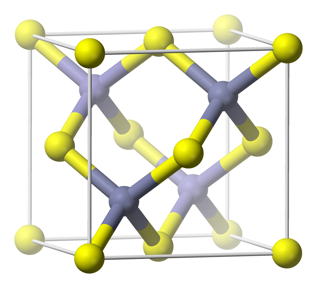
Aluminium gallium arsenide (also gallium aluminium arsenide) (AlxGa1−xAs) is a semiconductor material with very nearly the same lattice constant as GaAs, but a larger bandgap. The x in the formula above is a number between 0 and 1 - this indicates an arbitrary alloy between GaAs and AlAs.

The chemical formula AlGaAs should be considered an abbreviated form of the above, rather than any particular ratio.

The bandgap varies between 1.42 eV (GaAs) and 2.16 eV (AlAs). For x < 0.4, the bandgap is direct.

The refractive index is related with the bandgap via the Kramers–Kronig relations and varies between 2.9 (x = 1) and 3.5 (x = 0). This allows the construction of Bragg mirrors used in VCSELs, RCLEDs, and substrate-transferred crystalline coatings.

Aluminium gallium arsenide is used as a barrier material in GaAs based heterostructure devices. The AlGaAs layer confines the electrons to a gallium arsenide region. An example of such a device is a quantum well infrared photodetector (QWIP).

It is commonly used in GaAs-based red- and near-infra-red-emitting (700–1100 nm) double-hetero-structure laser diodes.

Safety and toxicity aspects

[edit]

The toxicology of AlGaAs has not been fully investigated. The dust is an irritant to skin, eyes and lungs. The environment, health and safety aspects of aluminium gallium arsenide sources (such as trimethylgallium and arsine) and industrial hygiene monitoring studies of standard MOVPE sources have been reported recently in a review.[1]

References

[edit]
[edit]
Revisions and contributorsEdit on WikipediaRead on Wikipedia
from Grokipedia
Aluminium gallium arsenide (AlGaAs), with the chemical formula AlxGa1-xAs where x ranges from 0 to 1, is a ternary III-V semiconductor alloy composed of gallium arsenide (GaAs) and aluminium arsenide (AlAs). It crystallizes in the zincblende structure and exhibits a tunable direct bandgap that varies from 1.424 eV for pure GaAs (x=0) to 2.168 eV for pure AlAs (x=1), transitioning to an indirect bandgap around x ≈ 0.45 at approximately 1.98 eV. This material's lattice constant closely matches that of GaAs (about 5.653 Å at x=0, with minimal mismatch of ~0.2% across compositions), enabling the epitaxial growth of high-quality heterostructures. AlGaAs is prized for its high thermal conductivity, chemical stability, and mechanical strength, making it a cornerstone in optoelectronic and high-frequency devices. The alloy's bandgap tunability allows precise control over emission wavelengths, particularly in the red and infrared spectrum (roughly 650 nm to 870 nm), which is essential for applications like light-emitting diodes (LEDs) used in red lighting such as traffic signals, and laser diodes used in readers, DVD players, and fiber optic communications. In heterostructure devices, AlGaAs serves as a barrier layer to confine electrons in GaAs channels, enhancing performance in high-electron-mobility transistors (HEMTs), quantum wells, superlattices, and solar cells. Its role extends to vertical-cavity surface-emitting lasers (VCSELs) and resonant-cavity LEDs (RCLEDs), where it forms Bragg mirrors due to its refractive index contrast with GaAs. Additionally, AlGaAs finds use in photodetectors and high-power, high-temperature electronics, leveraging its wider bandgap compared to GaAs for improved and efficiency in and photonic applications.

Composition and crystal structure

Chemical composition

Aluminium gallium arsenide (AlGaAs) is a ternary III-V semiconductor alloy composed of aluminium, gallium, and arsenic elements. Its chemical formula is AlxGa1xAs\mathrm{Al}_x \mathrm{Ga}_{1-x} \mathrm{As}, where the subscript xx denotes the molar fraction of aluminium substituting for gallium. The value of xx varies continuously from 0 to 1, enabling a wide range of alloy compositions. At x=0x = 0, the material is pure gallium arsenide (GaAs), a binary compound of gallium and arsenic known for its direct bandgap and applications in optoelectronics. At x=1x = 1, it becomes pure aluminium arsenide (AlAs), another binary III-V compound with distinct electronic properties. These binary endpoints serve as the parent compounds for the AlGaAs alloy system. The fraction xx plays a crucial role in tailoring the material's properties, particularly by modifying the bandgap energy and enabling near-perfect lattice matching to GaAs substrates across the composition range. This tunability arises from the similar atomic sizes of and gallium, which minimize strain in heterostructures grown on GaAs. AlGaAs typically adopts the zincblende , consistent with its binary constituents.

Crystal structure and lattice parameters

Aluminium gallium arsenide (AlxGa1-xAs) crystallizes in the zincblende structure, the same cubic lattice adopted by its binary constituents GaAs and AlAs, with space group Td2-F¯43*m. This structure features a face-centered cubic arrangement of the anion (As) sublattice, with the cation (Al and Ga) atoms tetrahedrally coordinated to four arsenic atoms, resulting in no inversion symmetry and important implications for piezoelectric and optical properties. The a of AlxGa1-xAs follows approximately, varying linearly with the aluminum mole fraction x as a=5.6533+0.0078xa = 5.6533 + 0.0078x , where x ranges from 0 (pure GaAs) to 1 (pure AlAs). For x = 0, a ≈ 5.653 , while for x = 1, a ≈ 5.661 , reflecting the slightly larger lattice of AlAs compared to GaAs. Although small deviations from linearity exist due to bonding effects, the linear approximation suffices for most epitaxial applications. This compositional dependence enables pseudomorphic epitaxial growth of AlGaAs layers on GaAs substrates, where the epilayer conforms to the substrate lattice without dislocations for low x. The relative lattice mismatch Δa/a=(aAlGaAsaGaAs)/aGaAs0.138%×x\Delta a / a = (a_{\text{AlGaAs}} - a_{\text{GaAs}}) / a_{\text{GaAs}} \approx 0.138\% \times x, remaining below 0.1% for x up to approximately 0.3 (mismatch ≈ 0.04%), which supports coherent interfaces critical for high-performance heterostructures. Beyond this range, strain relaxation via misfit dislocations can occur, limiting layer thickness to the critical value determined by Matthews-Blakeslee .

Synthesis and fabrication

Growth techniques

Aluminium gallium arsenide (AlGaAs) layers are primarily produced through epitaxial growth techniques that enable the deposition of high-quality crystalline films on suitable substrates, such as GaAs for lattice-matched compositions. Among these, metalorganic vapor phase epitaxy (MOVPE), also known as metalorganic (MOCVD), stands as the dominant method due to its scalability and ability to produce uniform layers over large areas. In MOVPE, AlGaAs is grown by transporting metalorganic in a carrier gas, typically , over a heated substrate in a reactor at atmospheric or reduced pressure. The key include trimethylaluminum (TMAl) for aluminum, trimethylgallium (TMGa) for , and (AsH₃) for , with growth temperatures ranging from 600°C to 800°C to ensure efficient decomposition and incorporation while minimizing defects. This technique allows for precise control of alloy composition by adjusting the precursor flow ratios, resulting in smooth, low-defect layers suitable for device applications. Molecular beam epitaxy (MBE) offers superior precision for ultrathin layers, enabling monolayer-level control through the sequential evaporation of elemental sources in an environment, typically at pressures of 10⁻¹⁰ to 10⁻¹¹ . Elemental , aluminum, and are sublimed from effusion cells, directed as molecular beams onto the substrate held at 500–650°C, allowing monitoring via reflection high-energy electron diffraction (RHEED) for abrupt interfaces and high purity. MBE is particularly valued for and high-performance devices requiring minimal impurities and sharp heterostructures. Liquid phase (LPE) involves the of AlGaAs from a molten solution, often a Ga-rich melt saturated with aluminum and , onto a substrate at temperatures around 700–850°C, making it suitable for thicker layers (several micrometers) compared to the thinner films from MOVPE or MBE. Although capable of yielding high-purity through careful melt purification, LPE is less commonly used today due to challenges in achieving uniform composition and thickness control, as well as lower reproducibility relative to gas-phase methods. Emerging techniques include electrochemical deposition, a cost-effective method for synthesizing nanostructured AlGaAs/GaAs heterostructures, such as nanowhiskers on GaAs substrates. Reported as of 2023, this approach enables the formation of high-quality "desert rose" nanocrystallites with good adhesion and potential for advanced electronic and optoelectronic applications.

Doping and alloying

Doping in aluminium gallium arsenide (AlGaAs) is essential for tailoring its electrical properties, with n-type and p-type impurities introduced during epitaxial growth to control carrier concentrations. N-type doping is commonly achieved using silicon (Si) or tellurium (Te), enabling donor concentrations up to 101910^{19} cm3^{-3}. Silicon, as a group IV dopant, primarily occupies gallium sites to donate electrons, particularly in growth techniques like molecular beam epitaxy (MBE) or metalorganic vapor phase epitaxy (MOVPE). Tellurium, a group VI element, serves as an alternative n-type dopant, offering reduced compensation compared to silicon in certain compositions. P-type doping in AlGaAs employs (Zn) or (Be), both group II elements that substitute on gallium sites to provide acceptors. is widely used due to its compatibility with vapor-phase growth methods, while is preferred in MBE for its low and high incorporation efficiency. can exhibit amphoteric behavior at high growth temperatures, acting as an acceptor on sites in addition to its donor role, which requires careful control of deposition conditions to minimize compensation. Alloying in AlGaAs involves adjusting the aluminum xx in AlxGa1xAs\mathrm{Al}_x\mathrm{Ga}_{1-x}\mathrm{As} during growth to precisely tune the bandgap , which varies from 1.42 eV for GaAs (x=0x=0) to 2.16 eV for AlAs (x=1x=1). This compositional control enables direct bandgap materials for x<0.45x < 0.45 and indirect for higher xx, facilitating integration in optoelectronic devices. Graded compositions, where xx varies continuously across layers, are employed in heterostructures to create smooth band profiles that reduce interface defects and enhance carrier confinement.

Physical and thermal properties

Density and mechanical properties

The density of aluminium gallium arsenide (AlGaAs), denoted as AlxGa1-xAs, decreases linearly with increasing aluminium content x, spanning from 5.32 g/cm³ for pure GaAs (x=0) to 3.76 g/cm³ for pure AlAs (x=1). This variation arises primarily from the lower of compared to , within the shared zincblende crystal structure. AlGaAs displays elastic properties typical of III-V compound semiconductors, with Young's modulus ranging from approximately 85 GPa for GaAs-like compositions to 110 GPa for AlAs-like compositions, influenced by the directional dependence in the cubic lattice. These materials exhibit inherent , lacking significant due to their strong covalent bonding and limited slip systems, which restricts deformation under stress. Vickers hardness of epitaxial AlGaAs films decreases with x, following an approximately linear trend of (6.9 - 2.2x) GPa, from about 6.9 GPa at x=0 to 4.7 GPa at x=1. , measured as KIC, similarly shows a linear increase with aluminium content, though values are generally low (on the order of 0.3-0.5 MPa·m1/2 for similar III-V films), rendering the material prone to crack propagation. In epitaxial layers, mechanical integrity is particularly sensitive to growth-induced defects such as dislocations and internal stresses, which can lower effective toughness by up to 25% and promote premature failure during processing or device fabrication.

Thermal expansion and conductivity

Aluminium gallium arsenide (AlxGa1-xAs) exhibits a linear of that decreases with increasing aluminum fraction x, from 5.7 × 10⁻⁶ K-1 at x=0 to 4.2 × 10⁻⁶ K-1 at x=1. This composition-dependent behavior follows and arises from the differing atomic bonding strengths in GaAs and AlAs end members. In heterostructures, the mismatch in coefficients between AlGaAs layers and GaAs substrates induces biaxial strain during cooling from epitaxial growth temperatures (typically 600–800°C), which can alter band alignments and carrier confinement. The thermal conductivity of AlGaAs at is 0.46 W/cm·K for x=0, decreasing to 0.23 W/cm·K for x=1, primarily due to enhanced from mass and force constant disorder in the lattice. This reduction is most pronounced at intermediate compositions (e.g., x ≈ 0.5), where alloy scattering limits heat dissipation. In high-power optoelectronic devices like diodes and high-electron-mobility transistors, the relatively low thermal conductivity necessitates advanced heat sinking and substrate choices (e.g., or SiC) to mitigate self-heating and maintain performance stability.

Electronic properties

Band structure and bandgap

Aluminium gallium arsenide (Alx_xGa1x_{1-x}As) exhibits a , with its featuring a valence band maximum at the Γ\Gamma point of the and a conduction band whose minimum varies with the aluminium composition xx. For low xx values, the conduction band minimum lies at the Γ\Gamma point, resulting in a direct bandgap similar to that of GaAs. As xx increases, the Γ\Gamma minimum rises in energy relative to the X-point minimum along the Λ\Lambda direction, leading to a crossover where the X point becomes the lowest conduction band edge. The valence band, comprising heavy-hole and light-hole subbands, remains relatively flat with its maximum at Γ\Gamma, showing minimal dispersion changes across the composition range. The bandgap energy Eg(x)E_g(x) of Alx_xGa1x_{1-x}As depends strongly on xx and transitions from direct to indirect character. For 0x<0.450 \leq x < 0.45, the bandgap is direct at the Γ\Gamma point, given by Eg(x)=1.424+1.247x(eV, at 300 K),E_g(x) = 1.424 + 1.247x \quad \text{(eV, at 300 K)}, spanning from 1.424 eV (GaAs at x=0x=0) to approximately 1.98 eV near the crossover. Beyond x0.45x \approx 0.45, the bandgap becomes indirect at the X point, with the energy described by Eg(x)=1.9+0.125x+0.143x2(eV, at 300 K),E_g(x) = 1.9 + 0.125x + 0.143x^2 \quad \text{(eV, at 300 K)}, reaching 2.16 eV for AlAs at x=1x=1. The precise crossover occurs at xc0.41x_c \approx 0.41 for Γ\Gamma-X and xc0.47x_c \approx 0.47 for Γ\Gamma-L, influencing the material's optoelectronic suitability. The bandgap exhibits a temperature dependence typical of III-V semiconductors, decreasing with increasing temperature due to electron-phonon interactions and thermal expansion. Near room temperature (around 300 K), EgE_g reduces at a rate of approximately 0.4-0.4 to 0.6-0.6 meV/K, varying slightly with xx; for example, values around 0.5-0.5 meV/K are reported for compositions in the direct regime. This shift is modeled using empirical relations like the Varshni equation, Eg(T)=Eg(0)αT2T+βE_g(T) = E_g(0) - \frac{\alpha T^2}{T + \beta}, with parameters α5×10⁴\alpha \approx 5 \times 10^{-4} eV/K and β200\beta \approx 200 K adapted from GaAs-like behavior.

Carrier transport properties

Carrier transport in aluminium gallium arsenide (AlGaAs) is characterized by high electron mobility in compositions with low aluminium content (x ≈ 0), reaching up to 8500 cm²/V·s at 300 K in undoped material, which approaches that of pure GaAs. This mobility decreases with increasing x due to enhanced alloy disorder scattering, following an approximate relation μ_n ≈ 8000 - 22000x + 10000x² cm²/V·s for 0 < x < 0.45 at room temperature. Hole mobility is significantly lower, typically around 400 cm²/V·s for low x, with a composition dependence given by μ_p ≈ 370 - 970x + 740x² cm²/V·s. These values reflect the material's suitability for high-speed electron transport while limiting hole-dominated applications. The electrical conductivity of AlGaAs is highly tunable through doping, transitioning from high-resistivity insulating behavior in undoped samples to low-resistivity semiconducting states. For n-type doping with donor concentrations on the order of 10^{18} cm^{-3}, resistivities as low as 10^{-3} Ω·cm can be achieved, particularly in low-x compositions where mobility remains high. This tunability arises from the incorporation of shallow donors like , enabling precise control over carrier density and enabling conductive layers in heterostructures. Impact ionization in AlGaAs involves electron and hole coefficients that increase with electric field and vary with Al content; for example, at x = 0.3, the threshold fields are approximately 7.6 × 10^5 V/cm for electrons and 8.5 × 10^5 V/cm for holes at 300 K. The avalanche breakdown field ranges from 4 to 6 × 10^5 V/cm, depending on doping (e.g., 4.5 × 10^5 V/cm for N_a = 10^{16} cm^{-3}), which exceeds that of silicon (≈ 3 × 10^5 V/cm) and supports applications in high-voltage power devices.

Optical properties

Refractive index

The refractive index of aluminium gallium arsenide (Alx_xGa1x_{1-x}As) is a key optical property that determines the phase velocity of light propagating through the material and influences its use in waveguides and photonic devices. For compositions spanning 0x10 \leq x \leq 1, the refractive index nn at a wavelength of 1 μ\mum decreases from approximately 3.5 (for x=0x=0, pure ) to 2.9 (for x=1x=1, pure AlAs), reflecting the material's tunability via alloying. This range arises from experimental measurements and empirical models fitted to spectroscopic data across the near-infrared spectrum. The wavelength dependence, or dispersion, of nn in AlGaAs is accurately captured by the Sellmeier equation, an empirical dispersion relation of the form n2(λ)=A+Bλ2λ2Cn^2(\lambda) = A + \frac{B \lambda^2}{\lambda^2 - C}, where λ\lambda is the vacuum wavelength and AA, BB, CC are composition-dependent coefficients derived from ellipsometry and reflectometry measurements. This model holds well below the direct band gap, typically for wavelengths longer than about 0.8 μ\mum depending on xx. As xx increases, nn decreases at fixed wavelength due to reduced electronic polarizability from the widening band gap, a connection enforced by the Kramers-Kronig relations that link the real part of the refractive index (dispersion) to the imaginary part (absorption) integrated over all frequencies. Shorter wavelengths also yield lower nn values, characteristic of normal dispersion in semiconductors away from absorption edges. In its unstrained cubic zincblende crystal structure, AlGaAs is optically isotropic with negligible intrinsic birefringence, as the symmetric lattice yields equal refractive indices for all polarizations. However, epitaxial films subjected to strain—such as biaxial compression or tension from lattice mismatch with substrates like GaAs or Si—induce photoelastic effects that split the refractive index for orthogonal polarizations, with birefringence magnitudes up to 10310^{-3} reported in strained heterostructures. This strain-induced anisotropy must be accounted for in device designs involving quantum wells or distributed Bragg reflectors.

Absorption and luminescence

Aluminium gallium arsenide (AlGaAs) exhibits distinct absorption characteristics that depend on its aluminum composition xx, particularly the transition between direct and indirect bandgap regimes. In the direct bandgap regime where x<0.45x < 0.45, the absorption coefficient α\alpha near the bandgap exceeds 10410^4 cm1^{-1}, typically reaching values around 2×1042 \times 10^4 cm1^{-1} for compositions such as x=0.20x = 0.20 at cryogenic temperatures. This strong absorption enables the use of thin-film structures for efficient light interaction in optoelectronic applications. For x>0.45x > 0.45 in the indirect bandgap regime, absorption near the band edge is significantly weaker due to the involvement of phonon-assisted transitions, resulting in lower α\alpha values that limit direct optical processes. Photoluminescence (PL) in AlGaAs is highly efficient in the direct bandgap regime (x<0.45x < 0.45), where internal quantum efficiencies can approach 99.7%, attributed to the favorable momentum conservation for radiative recombination. The emission wavelength is tunable by varying xx in the direct bandgap regime (x<0.45x < 0.45), spanning approximately 630–870 nm, corresponding to bandgap energies from about 1.98 eV (x0.45x \approx 0.45) to 1.42 eV (x=0x = 0) via the relation Eg=1.424+1.247xE_g = 1.424 + 1.247x eV. Note that practical efficiency is highest for lower xx (longer wavelengths), decreasing near the indirect transition. In contrast, PL efficiency diminishes in the indirect regime (x>0.45x > 0.45) due to slower radiative rates and competing nonradiative pathways. The exciton binding energy in bulk AlGaAs is approximately 5 meV, which plays a key role in room-temperature performance by allowing to persist despite thermal dissociation (kT ≈ 25 meV), thereby supporting efficient even at elevated temperatures. This value influences the linewidth and intensity of PL spectra and increases to around 10 meV in quantum-confined structures due to enhancement from reduced dimensionality.

Applications

Optoelectronic devices

Aluminium gallium arsenide (AlGaAs) serves as the primary material for cladding and barrier layers in GaAs/AlGaAs lasers, enabling efficient carrier and optical confinement due to its wider bandgap relative to (GaAs). In these structures, undoped GaAs forms the active region, typically 100 Å thick, sandwiched between AlGaAs barriers and graded-index separate-confinement heterostructure (GRIN-SCH) layers that guide both electrons and photons to the well, reducing threshold currents and improving overall efficiency. These lasers emit in the 780–850 nm wavelength range, which allows precise matching to application needs. Such lasers at 780 nm have been pivotal in (CD) players, where low-power operation (below 10 mW) and reliable single-mode emission facilitate data readout from optical media. For short-haul , 850 nm variants support multimode links in data centers and local area networks, offering high-speed modulation up to several gigabits per second with low noise. The heterostructure design minimizes losses, achieving internal quantum efficiencies exceeding 90% in optimized devices, though challenges like catastrophic optical damage limit continuous-wave powers to tens of milliwatts without advanced cooling. In vertical-cavity surface-emitting lasers (VCSELs), AlGaAs layers form the core of distributed Bragg reflectors (DBRs), consisting of alternating high- and low-refractive-index pairs of AlGaAs and GaAs (or AlAs) quarter-wave stacks that provide reflectivity over 99% for vertical light . This configuration yields circular, low-divergence output beams ideal for array integration and optical interconnects at 850 nm, with threshold currents as low as 1 mA in room-temperature devices grown on GaAs or even Si substrates. Resonant-cavity light-emitting diodes (RCLEDs) similarly utilize AlGaAs/GaAs DBRs on one or both sides of the cavity to enhance directionality and spectral purity, boosting external quantum efficiency to 20–30% for applications in short-range data transmission where lasing thresholds are undesirable. High-electron-mobility transistors (HEMTs) exploit the band offset at the AlGaAs/GaAs —approximately 0.3 eV for conduction band discontinuity—to form a high-mobility via modulation doping, where donors in the AlGaAs supply layer populate the undoped GaAs channel without impurities. This enables mobilities exceeding 10,000 cm²/V·s at 77 K, far surpassing bulk GaAs, and supports cutoff frequencies up to 100 GHz in early devices. In amplifiers, AlGaAs/GaAs HEMTs deliver low figures (below 1 dB) and high gain (10–15 dB) for systems and communications, with the heterostructure's abrupt interface minimizing intervalley for robust performance at power densities over 1 W/mm.

Photovoltaic and sensing devices

Aluminium gallium arsenide (AlGaAs) plays a critical role in multi-junction solar cells as the wide-bandgap material for the top subcell, where compositions such as Al0.3Ga0.7As provide a bandgap energy of approximately 1.8 eV, allowing efficient capture of high-energy photons while transmitting longer-wavelength light to underlying GaAs or InGaAs layers. This layered architecture enhances overall spectral utilization, particularly in under high illumination intensities, where device efficiencies have surpassed 30% under AM0 conditions. For instance, three-junction stacks incorporating an AlGaAs top cell have demonstrated 25.2% efficiency at 1-sun AM0 illumination, with more recent designs achieving efficiencies exceeding 32% under AM0 conditions as of ; potential for higher performance in concentrated due to improved junctions and reduced series resistance. In sensing applications, AlGaAs/GaAs infrared photodetectors (QWIPs) leverage intersubband transitions within modulation-doped s to achieve sensitive detection in the long-wave (LWIR) spectrum of 8-12 μm, ideal for thermal imaging in military and civilian contexts. These devices operate by exciting electrons from bound ground states to continuum states under perpendicular illumination, enabling high quantum efficiency and uniform response in large-format focal plane arrays, such as 640 × 512 configurations with peak detectivities exceeding 1010 cm Hz1/2/W at 77 K. The mature GaAs-based epitaxial growth processes further support scalable production of QWIP arrays for uncooled or cryogenically cooled systems. AlGaAs heterostructures also enable high-speed photodiodes for fiber optic systems, where the abrupt band offsets reduce carrier transit times and compared to homojunction designs, supporting bandwidths suitable for data rates beyond 40 Gbps. In particular, vertical dual-depletion-region photodetectors using AlGaAs/GaAs layers at 850 nm wavelengths have achieved 3 dB bandwidths of 46 GHz with low dark currents, benefiting from inductive peaking to extend high-frequency response without compromising around 0.5 A/W. These attributes make them valuable for short-haul optical interconnects in infrastructure.

Health and safety

Toxicity and hazards

Aluminium gallium arsenide (AlGaAs), with a composition featuring 50 at% in its formula \ceAlxGa1xAs\ce{Al_x Ga_{1-x} As}, exhibits primarily attributable to its content, akin to that observed in (GaAs). Inhalation of AlGaAs dust leads to respiratory irritation and pneumotoxicity, as demonstrated in intratracheal instillation studies in animal models where AlGaAs caused and damage, though to a lesser extent than GaAs or . Chronic exposure to such arsenic-based III-V semiconductors is linked to carcinogenic risks, including skin and , due to the established carcinogenicity of inorganic compounds released upon dissolution or metabolism. No dedicated LD50 data exist for AlGaAs via common exposure routes like or ingestion, but its toxicity profile is considered analogous to other III-V arsenides, with intraperitoneal LD50 values for GaAs reported at 10 g/kg in rats and 4.7 g/kg in mice. AlGaAs is reactive and can decompose upon contact with moisture or —albeit slowly—to release toxic compounds, possibly including gas (\ceAsH3\ce{AsH3}), a potent hepatotoxin and that inhibits and can lead to rapid systemic poisoning, multi-organ failure, and death even at low concentrations. This hazard is exacerbated under conditions of heating or exposure to acids, generating additional toxic fumes.

Handling and disposal

When handling aluminium gallium arsenide (AlGaAs) materials, particularly during fabrication processes, appropriate (PPE) is essential to minimize exposure to dust and particles, which can release compounds. Recommended PPE includes gloves to prevent skin contact, safety goggles to protect the eyes, and respirators with appropriate filters for airborne particulates, especially in environments where or cutting may generate dust. All manipulations should occur in a well-ventilated to contain potential toxic fumes, particularly if the material is exposed to acids or high temperatures that could liberate gas. AlGaAs waste is classified as hazardous due to its content and must be managed in accordance with regulations such as the , which designates arsenic-bearing wastes as toxic under characteristic code D004. Preferred disposal methods include high-temperature in permitted facilities to destroy organic components and immobilize arsenic, or stabilization through chemical fixation (e.g., with or lime) to prevent leaching, rather than direct landfilling, which is restricted to minimize contamination. Improper disposal of AlGaAs can release into ecosystems, leading to in aquatic organisms and food chains, where it biomagnifies and poses risks to and through contaminated and . To mitigate environmental impacts, techniques such as epitaxial lift-off (ELO) are employed, allowing separation of AlGaAs device layers from reusable substrates via selective etching of a sacrificial layer, thereby reducing waste generation and resource consumption. This process has been demonstrated to enable multiple substrate reuses in III-V production, supporting sustainable manufacturing practices.

References

Add your contribution
Related Hubs
User Avatar
No comments yet.