
Community hub
Recent from talks
Contribute something
Nothing was collected or created yet.
GeForce 600 series
View on Wikipedia
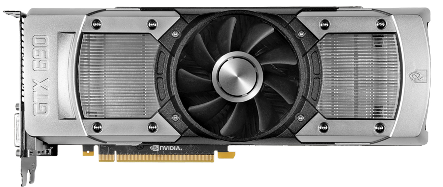
 A GeForce GTX 690 released in 2012, the series' flagship model | |
| Release date | March 22, 2012 |
|---|---|
| Codename | GK10x |
| Architecture | |
| Models | GeForce series
|
| Transistors | 292M 40 nm (GF119)
|
| Cards | |
| Entry-level |
|
| Mid-range |
|
| High-end |
|
| Enthusiast |
|
| API support | |
| OpenCL | OpenCL 3.0[a] |
| OpenGL | OpenGL 4.6 |
| Vulkan | Vulkan 1.2[2] SPIR-V |
| DirectX | Direct3D 12.0 (feature level 11_0)[1] Shader Model 6.5 |
| History | |
| Predecessor | GeForce 500 series |
| Successor | |
| Support status | |
| Unsupported | |
The GeForce 600 series is a series of graphics processing units developed by Nvidia, first released in 2012. It served as the introduction of the Kepler architecture. It is succeeded by the GeForce 700 series.
Overview
[edit]Where the goal of the previous architecture, Fermi, was to increase raw performance (particularly for compute and tessellation), Nvidia's goal with the Kepler architecture was to increase performance per watt, while still striving for overall performance increases.[3] The primary way Nvidia achieved this goal was through the use of a unified clock. By abandoning the shader clock found in their previous GPU designs, efficiency is increased, even though it requires more cores to achieve similar levels of performance. This is not only because the cores are more power efficient (two Kepler cores using about 90% of the power of one Fermi core, according to Nvidia's numbers), but also because the reduction in clock speed delivers a 50% reduction in power consumption in that area.[4]
Kepler also introduced a new form of texture handling known as bindless textures. Previously, textures needed to be bound by the CPU to a particular slot in a fixed-size table before the GPU could reference them. This led to two limitations: one was that because the table was fixed in size, there could only be as many textures in use at one time as could fit in this table (128). The second was that the CPU was doing unnecessary work: it had to load each texture, and also bind each texture loaded in memory to a slot in the binding table.[3] With bindless textures, both limitations are removed. The GPU can access any texture loaded into memory, increasing the number of available textures and removing the performance penalty of binding.
Finally, with Kepler, Nvidia was able to increase the memory clock to 6 GHz. To accomplish this, Nvidia needed to design an entirely new memory controller and bus. While still shy of the theoretical 7 GHz limitation of GDDR5, this is well above the 4 GHz speed of the memory controller for Fermi.[4]
Kepler is named after the German mathematician, astronomer, and astrologer Johannes Kepler.
Architecture
[edit]The GeForce 600 series contains products from both the older Fermi and newer Kepler generations of Nvidia GPUs. Kepler based members of the 600 series add the following standard features to the GeForce family:
- PCI Express 3.0 interface
- DisplayPort 1.2
- HDMI 1.4a 4K x 2K video output
- Purevideo VP5 hardware video acceleration (up to 4K x 2K H.264 decode)
- Hardware H.264 encoding acceleration block (NVENC)
- Support for up to 4 independent 2D displays, or 3 stereoscopic/3D displays (NV Surround)
- Next Generation Streaming Multiprocessor (SMX)
- A New Instruction Scheduler
- Bindless Textures
- CUDA Compute Capability 3.0
- GPU Boost
- TXAA
- Manufactured by TSMC on a 28 nm process
Streaming Multiprocessor Architecture (SMX)
[edit]The Kepler architecture employs a new Streaming Multiprocessor Architecture called SMX. The SMX are the key method for Kepler's power efficiency as the whole GPU uses a single "Core Clock" rather than the double-pump "Shader Clock".[4] The SMX usage of a single unified clock increases the GPU power efficiency due to the fact that two Kepler CUDA Cores consume 90% power of one Fermi CUDA Core. Consequently, the SMX needs additional processing units to execute a whole warp per cycle. Kepler also needed to increase raw GPU performance as to remain competitive. As a result, it doubled the CUDA Cores from 16 to 32 per CUDA array, 3 CUDA Cores Array to 6 CUDA Cores Array, 1 load/store and 1 SFU group to 2 load/store and 2 SFU group. The GPU processing resources are also double. From 2 warp schedulers to 4 warp schedulers, 4 dispatch unit became 8 and the register file doubled to 64K entries as to increase performance. With the doubling of GPU processing units and resources increasing the usage of die spaces, The capability of the PolyMorph Engine aren't double but enhanced, making it capable of spurring out a polygon in 2 cycles instead of 4.[5] With Kepler, Nvidia not only worked on power efficiency but also on area efficiency. Therefore, Nvidia opted to use eight dedicated FP64 CUDA cores in a SMX as to save die space, while still offering FP64 capabilities since all Kepler CUDA cores are not FP64 capable. With the improvement Nvidia made on Kepler, the results include an increase in GPU graphic performance while downplaying FP64 performance.
A new instruction scheduler
[edit]Additional die areas are acquired by replacing the complex hardware scheduler with a simple software scheduler. With software scheduling, warps scheduling was moved to Nvidia's compiler and as the GPU math pipeline now has a fixed latency, it now include the utilization of instruction-level parallelism and superscalar execution in addition to thread-level parallelism. As instructions are statically scheduled, scheduling inside a warp becomes redundant since the latency of the math pipeline is already known. This resulted an increase in die area space and power efficiency.[4][6][3]
GPU Boost
[edit]GPU Boost is a new feature which is roughly analogous to turbo boosting of a CPU. The GPU is always guaranteed to run at a minimum clock speed, referred to as the "base clock". This clock speed is set to the level which will ensure that the GPU stays within TDP specifications, even at maximum loads.[3] When loads are lower, however, there is room for the clock speed to be increased without exceeding the TDP. In these scenarios, GPU Boost will gradually increase the clock speed in steps, until the GPU reaches a predefined power target (which is 170W by default).[4] By taking this approach, the GPU will ramp its clock up or down dynamically, so that it is providing the maximum amount of speed possible while remaining within TDP specifications.
The power target, as well as the size of the clock increase steps that the GPU will take, are both adjustable via third-party utilities and provide a means of overclocking Kepler-based cards.[3]
Microsoft DirectX support
[edit]Both Fermi and Kepler based cards support Direct3D 11, both also support Direct3D 12, though not all features provided by the API.[7][8]
TXAA
[edit]Exclusive to Kepler GPUs, TXAA is a new anti-aliasing method from Nvidia that is designed for direct implementation into game engines. TXAA is based on the MSAA technique and custom resolve filters. Its design addresses a key problem in games known as shimmering or temporal aliasing; TXAA resolves that by smoothing out the scene in motion, making sure that any in-game scene is being cleared of any aliasing and shimmering.[9]
NVENC
[edit]NVENC is Nvidia's SIP block that performs video encoding, in a way similar to Intel's Quick Sync Video and AMD's VCE. NVENC is a power-efficient fixed-function pipeline that is able to take codecs, decode, preprocess, and encode H.264-based content. NVENC specification input formats are limited to H.264 output. But still, NVENC, through its limited format, can perform encoding in resolutions up to 4096×4096.[10]
Like Intel's Quick Sync, NVENC is currently exposed through a proprietary API, though Nvidia does have plans to provide NVENC usage through CUDA.[10]
New driver features
[edit]In the R300 drivers, released alongside the GTX 680, Nvidia introduced a new feature called Adaptive VSync. This feature is intended to combat the limitation of v-sync that, when the framerate drops below 60 FPS, there is stuttering as the v-sync rate is reduced to 30 FPS, then down to further factors of 60 if needed. However, when the framerate is below 60 FPS, there is no need for v-sync as the monitor will be able to display the frames as they are ready. To address this issue (while still maintaining the advantages of v-sync with respect to screen tearing), Adaptive VSync can be turned on in the driver control panel. It will enable VSync if the framerate is at or above 60 FPS, while disabling it if the framerate lowers. Nvidia claims that this will result in a smoother overall display.[3]
While the feature debuted alongside the GTX 680, this feature is available to users of older Nvidia cards who install the updated drivers.[3]
Dynamic Super Resolution (DSR) was added to Fermi and Kepler GPUs with an October 2014 release of Nvidia drivers. This feature aims at increasing the quality of displayed picture, by rendering the scenery at a higher and more detailed resolution (upscaling), and scaling it down to match the monitor's native resolution (downsampling).[11] Such feature is similar to AMD's Virtual Super Resolution (VSR).
History
[edit]In September 2010, Nvidia first announced Kepler.[12]
In early 2012, details of the first members of the 600 series parts emerged. These initial members were entry-level laptop GPUs sourced from the older Fermi architecture.
On March 22, 2012, Nvidia unveiled the 600 series GPU: the GTX 680 for desktop PCs and the GeForce GT 640M, GT 650M, and GTX 660M for notebook/laptop PCs.[13][14]
On April 29, 2012, the GTX 690 was announced as the first dual-GPU Kepler product.[15]
On May 10, 2012, the GTX 670 was officially announced.[16]
On June 4, 2012, the GTX 680M was officially announced.[17]
On August 16, 2012, the GTX 660 Ti was officially announced.[18]
On September 13, 2012, the GTX 660 and GTX 650 were officially announced.[19]
On October 9, 2012, the GTX 650 Ti was officially announced.[20]
On March 26, 2013, the GTX 650 Ti BOOST was officially announced.[21]
Products
[edit]GeForce 600 (6xx) series
[edit]
- 1 SPs – Shader Processors – Unified Shaders : Texture mapping units : Render output units
- 2 The GeForce 605 (OEM) card is a rebranded GeForce 510.
- 3 The GeForce GT 610 card is a rebranded GeForce GT 520.
- 4 The GeForce GT 620 (OEM) card is a rebranded GeForce GT 520.
- 5 The GeForce GT 620 card is a rebranded GeForce GT 530.
- 6 This revision of GeForce GT 630 (DDR3) card is a rebranded GeForce GT 440 (DDR3).
- 7 The GeForce GT 630 (GDDR5) card is a rebranded GeForce GT 440 (GDDR5).
- 8 The GeForce GT 640 (OEM) card is a rebranded GeForce GT 545 (DDR3).
- 9 The GeForce GT 645 (OEM) card is a rebranded GeForce GTX 560 SE.
GeForce 600M (6xxM) series
[edit]The GeForce 600M series for notebooks architecture. The processing power is obtained by multiplying shader clock speed, the number of cores and how many instructions the cores are capable of performing per cycle.
| Model | Launch | Code Name | Fab (nm) | Bus interface | Core Configuration1 | Clock Speed | Fillrate | Memory | API Support (version) | Processing Power2 (GFLOPS) |
TDP (Watts) | Notes | |||||||||
|---|---|---|---|---|---|---|---|---|---|---|---|---|---|---|---|---|---|---|---|---|---|
| Core (MHz) | Shader (MHz) | Memory (MT/s) | Pixel (GP/s) | Texture (GT/s) | Size (MiB) | Bandwidth (GB/s) | DRAM Type | Bus Width (bit) | DirectX | OpenGL | OpenCL | Vulkan | |||||||||
| GeForce 610M[22] | Dec 2011 | GF119 (N13M-GE) | 40 | PCIe 2.0 x16 | 48:8:4 | 450 | 900 | 1800 | 3.6 | 7.2 | 1024 2048 |
14.4 | DDR3 | 64 | 12.0 (11_0) | 4.6 | 1.1 | N/a | 142.08 | 12 | OEM. Rebadged GT 520MX |
| GeForce GT 620M[23] | Apr 2012 | GF117 (N13M-GS) | 28 | 96:16:4 | 625 | 1250 | 1800 | 2.5 | 10 | 14.4 28.8 |
64 128 |
240 | 15 | OEM. Die-Shrink GF108 | |||||||
| GeForce GT 625M | October 2012 | GF117 (N13M-GS) | 14.4 | 64 | |||||||||||||||||
| GeForce GT 630M[23][24][25] | Apr 2012 | GF108 (N13P-GL) GF117 |
40 28 |
660 800 |
1320 1600 |
1800 4000 |
2.6 3.2 |
10.7 12.8 |
28.8 32.0 |
DDR3 GDDR5 |
128 64 |
258.0 307.2 |
33 | GF108: OEM. Rebadged GT 540M GF117: OEM Die-Shrink GF108 | |||||||
| GeForce GT 635M[23][26][27] | Apr 2012 | GF106 (N12E-GE2) GF116 |
40 | 144:24:24 | 675 | 1350 | 1800 | 16.2 | 16.2 | 2048 1536 |
28.8 43.2 |
DDR3 | 128 192 |
289.2 388.8 |
35 | GF106: OEM. Rebadged GT 555M GF116: 144 Unified Shaders | |||||
| GeForce GT 640M LE[23] | March 22, 2012 | GF108 GK107 (N13P-LP) |
40 28 |
PCIe 2.0 x16 PCIe 3.0 x16 |
96:16:4 384:32:16 |
762 500 |
1524 500 |
3130 1800 |
3 8 |
12.2 16 |
1024 2048 |
50.2 28.8 |
GDDR5 DDR3 |
128 | 1.1 1.2 |
N/A ? |
292.6 384 |
32 20 |
GF108: Fermi GK107: Kepler architecture | ||
| GeForce GT 640M[23][28] | March 22, 2012 | GK107 (N13P-GS) | 28 | PCIe 3.0 x16 | 384:32:16 | 625 | 625 | 1800 4000 |
10 | 20 | 28.8 64.0 |
DDR3 GDDR5 |
1.2 | 1.1 | 480 | 32 | Kepler architecture | ||||
| GeForce GT 645M | October 2012 | GK107 (N13P-GS) | 710 | 710 | 1800 4000 |
11.36 | 22.72 | 545 | |||||||||||||
| GeForce GT 650M[23][29][30] | March 22, 2012 | GK107 (N13P-GT) | 835 745 900* |
950 835 900* |
1800 4000 5000* |
15.2 13.4 14.4* |
30.4 26.7 28.8* |
1024 2048 * |
28.8 64.0 80.0* |
DDR3 GDDR5 GDDR5* |
729.6 641.3 691.2* |
45 | Kepler architecture | ||||||||
| GeForce GTX 660M[23][30][31][32] | March 22, 2012 | GK107 (N13E-GE) | 835 | 950 | 5000 | 15.2 | 30.4 | 2048 | 80.0 | GDDR5 | 729.6 | 50 | Kepler architecture | ||||||||
| GeForce GTX 670M[23] | April 2012 | GF114 (N13E-GS1-LP) | 40 | PCIe 2.0 x16 | 336:56:24 | 598 | 1196 | 3000 | 14.35 | 33.5 | 1536 3072 |
72.0 | 192 | 1.1 | N/a | 803.6 | 75 | OEM. Rebadged GTX 570M | |||
| GeForce GTX 670MX | October 2012 | GK106 (N13E-GR) | 28 | PCIe 3.0 x16 | 960:80:24 | 600 | 600 | 2800 | 14.4 | 48.0 | 67.2 | 1.2 | 1.1 | 1152 | Kepler architecture | ||||||
| GeForce GTX 675M[23] | April 2012 | GF114 (N13E-GS1) | 40 | PCIe 2.0 x16 | 384:64:32 | 620 | 1240 | 3000 | 19.8 | 39.7 | 2048 | 96.0 | 256 | 1.1 | ? | 952.3 | 100 | OEM. Rebadged GTX 580M | |||
| GeForce GTX 675MX | October 2012 | GK106 (N13E-GSR) | 28 | PCIe 3.0 x16 | 960:80:32 | 600 | 600 | 3600 | 19.2 | 48.0 | 4096 | 115.2 | 1.2 | 1.1 | 1152 | Kepler architecture | |||||
| GeForce GTX 680M | June 4, 2012 | GK104 (N13E-GTX) | 1344:112:32 | 720 | 720 | 3600 | 23 | 80.6 | 1935.4 | ||||||||||||
| GeForce GTX 680MX | October 23, 2012 | GK104 | 1536:128:32 | 5000 | 92.2 | 160 | 2234.3 | 100+ | |||||||||||||
| Model | Launch | Code Name | Fab (nm) | Bus interface | Core Configuration1 | Clock Speed | Fillrate | Memory | API Support (version) | Processing Power2 (GFLOPS) |
TDP (Watts) | Notes | |||||||||
| Core (MHz) | Shader (MHz) | Memory (MT/s) | Pixel (GP/s) | Texture (GT/s) | Size (MiB) | Bandwidth (GB/s) | DRAM Type | Bus Width (bit) | DirectX | OpenGL | OpenCL | Vulkan | |||||||||
(*)-Apple MacBook Pro Retina 2012 with 512MB or 1024MB GDDR5 configuration.
Chipset table
[edit]GeForce 600 (6xx) series
[edit]| Model | Launch | Code name | Fab (nm) | Transistors (million) | Die size (mm2) | Bus interface | SM count | Core config[b] | Clock rate | Fillrate | Memory configuration | Supported API version | Processing power (GFLOPS)[c] | TDP (Watts) | Release price (USD) | ||||||||||||
|---|---|---|---|---|---|---|---|---|---|---|---|---|---|---|---|---|---|---|---|---|---|---|---|---|---|---|---|
| Core (MHz) | Average Boost (MHz) | Max Boost (MHz) | Shader (MHz) | Memory (MHz) | Pixel (GP/s) | Texture (GT/s) | Size (MB) | Bandwidth (GB/s) | DRAM type | Bus width (bit) | Vulkan[d] | Direct3D | OpenGL | OpenCL | Single precision | Double precision | |||||||||||
| GeForce 605[e] | April 3, 2012 | GF119 | TSMC 40 nm | 292 | 79 | PCIe 2.0 x16 | 1 | 48:8:4 | 523 | N/a | N/a | 1046 | 898 (1796) |
2.09 | 4.2 | 512 1024 | 14.4 | DDR3 | 64 | N/a | 12 (11_0) | 4.6 | 1.2 | 100.4 | Unknown | 25 | OEM |
| GeForce GT 610[f] | May 15, 2012 | GF119-300-A1 | PCIe 2.0 x16, PCIe x1, PCI | 48:8:4 | 810 | N/a | N/a | 1620 | 1000 1800 |
3.24 | 6.5 | 512 1024 2048 |
8 14.4 |
155.5 | Unknown | 29 | Retail | ||||||||||
| GeForce GT 620[g] | April 3, 2012 | GF119 | PCIe 2.0 x16 | 48:8:4 | N/a | N/a | 898 (1796) |
6.5 | 512 1024 |
14.4 | 155.5 | Unknown | 30 | OEM | |||||||||||||
| May 15, 2012 | GF108-100-KB-A1 | 585 | 116 | 2 | 96:16:4 | 700 | N/a | N/a | 1400 | 1000–1800 | 2.8 | 11.2 | 1024 2048 |
8–14.4 | 268.8 | Unknown | 49 | Retail | |||||||||
| GeForce GT 625 | February 19, 2013 | GF119 | 292 | 79 | 1 | 48:8:4 | 810 | N/a | N/a | 1620 | 898 (1796) |
3.24 | 6.5 | 512 1024 | 14.4 | 155.5 | Unknown | 30 | OEM | ||||||||
| GeForce GT 630[h][i] | April 24, 2012 | GK107 | TSMC 28 nm | 1300 | 118 | PCIe 3.0 x16 | 192:16:16 | 875 | N/a | N/a | 875 | 891 (1782) |
14 | 14 | 1024 2048 |
28.5 | 128 | 1.2 | 336 | 14 | 50 | ||||||
| May 15, 2012 | GF108-400-A1 | TSMC 40 nm | 585 | 116 | PCIe 2.0 x16 | 2 | 96:16:4 | 700 | N/a | N/a | 1620 | 1600–1800 | 2.8 | 11.2 | 1024 2048 4096 |
25.6–28.8 | N/a | 311 | Unknown | 49 | Retail | ||||||
| GF108 | 96:16:4 | 810 | N/a | N/a | 1620 | 800 (3200) |
3.2 | 13 | 1024 | 51.2 | GDDR5 | 311 | Unknown | 65 | |||||||||||||
| May 29, 2013 | GK208-301-A1 | TSMC 28 nm | 1020 | 79 | PCIe 2.0 x8 | 1 | 384:16:8 | 902 | N/a | N/a | 902 | 900 (1800) |
7.22 | 14.44 | 1024 2048 |
14.4 | DDR3 | 64 | 1.2 | 692.7 | Unknown | 25 | |||||
| GeForce GT 635 | February 19, 2013 | GK208 | PCIe 3.0 x8 | 384:16:8 | 967 | N/a | N/a | 967 | 1001 (2002) |
7.74 | 15.5 | 16 | 742.7 | Unknown | 35 | OEM | |||||||||||
| GeForce GT 640[j] | April 24, 2012 | GF116 | TSMC 40 nm | 1170 | 238 | PCIe 2.0 x16 | 3 | 144:24:24 | 720 | N/a | N/a | 1440 | 891 (1782) |
17.3 | 17.3 | 1536 3072 |
42.8 | 192 | N/a | 414.7 | Unknown | 75 | |||||
| GK107 | TSMC 28 nm | 1300 | 118 | PCIe 3.0 x16 | 2 | 384:32:16 | 797 | N/a | N/a | 797 | 891 (1782) |
12.8 | 25.5 | 1024 2048 |
28.5 | 128 | 1.2 | 612.1 | 25.50 | 50 | |||||||
| June 5, 2012 | 900 | N/a | N/a | 900 | 891 (1782) |
14.4 | 28.8 | 2048 4096 |
28.5 | 691.2 | 28.8 | 65 | 100 | ||||||||||||||
| April 24, 2012 | 950 | N/a | N/a | 950 | 1250 (5000) |
15.2 | 30.4 | 1024 2048 |
80 | GDDR5 | 729.6 | 30.40 | 75 | OEM | |||||||||||||
| May 29, 2013 | GK208-400-A1 | TSMC 28 nm | 1020 | 79 | PCIe 2.0 x8 | 384:16:8 | 1046 | N/a | N/a | 1046 | 1252 (5008) |
8.37 | 16.7 | 1024 | 40.1 | 64 | 803.3 | Unknown | 49 | ||||||||
| GeForce GT 645[k] | April 24, 2012 | GF114-400-A1 | TSMC 40 nm | 1950 | 332 | PCIe 2.0 x16 | 6 | 288:48:24 | 776 | N/a | N/a | 1552 | 1914 | 18.6 | 37.3 | 91.9 | 192 | N/a | 894 | Unknown | 140 | OEM | |||||
| GeForce GTX 645 | April 22, 2013 | GK106 | TSMC 28 nm | 2540 | 221 | PCIe 3.0 x16 | 3 | 576:48:16 | 823.5 | 888.5 | N/a | 823 | 1000 (4000) |
14.16 | 39.5 | 64 | 128 | 1.2 | 948.1 | 39.53 | 64 | ||||||
| GeForce GTX 650 | September 13, 2012 | GK107-450-A2 | 1300 | 118 | 2 | 384:32:16 | 1058 | N/a | N/a | 1058 | 1250 (5000) |
16.9 | 33.8 | 1024 2048 |
80 | 812.54 | 33.86 | 110 | |||||||||
| November 27, 2013[34] | GK-106-400-A1 | 2540 | 221 | N/a | 65 | ? | |||||||||||||||||||||
| GeForce GTX 650 Ti | October 9, 2012 | GK106-220-A1 | 4 | 768:64:16 | 928 | N/a | N/a | 928 | 1350 (5400) |
14.8 | 59.4 | 86.4 | 1425.41 | 59.39 | 110 | 150 (130) | |||||||||||
| GeForce GTX 650 Ti Boost | March 26, 2013 | GK106-240-A1 | 768:64:24 | 980 | 1032 | N/a | 980 | 1502 (6008) |
23.5 | 62.7 | 144.2 | 192 | 1505.28 | 62.72 | 134 | 170 (150) | |||||||||||
| GeForce GTX 660 | September 13, 2012 | GK106-400-A1 | 5 | 960:80:24 | 1084 | 1502 (6008) |
23.5 | 78.4 | 1536+512 3072 |
96.1+48.1 144.2 |
128+64 192 |
1881.6 | 78.40 | 140 | 230 (180) | ||||||||||||
| August 22, 2012 | GK104-200-KD-A2 | 3540 | 294 | 6 | 1152:96:24 1152:96:32 |
823.5 | 888.5 | 899 | 823 | 1450 (5800) |
19.8 | 79 | 1536 2048 3072 |
134 186 |
192 256 |
2108.6 | 79.06 | 130 | OEM | ||||||||
| GeForce GTX 660 Ti | August 16, 2012 | GK104-300-KD-A2 | 7 | 1344:112:24 | 915 | 980 | 1058 | 915 | 1502 (6008) |
22.0 | 102.5 | 2048 | 96.1+48.1 144.2 |
128+64 192 |
2459.52 | 102.48 | 150 | 300 | |||||||||
| GeForce GTX 670 | May 10, 2012 | GK104-325-A2 | 1344:112:32 | 1084 | 1502 (6008) |
29.3 | 102.5 | 2048 4096 |
192.256 | 256 | 2459.52 | 102.48 | 170 | 400 | |||||||||||||
| GeForce GTX 680 | March 22, 2012 | GK104-400-A2 | 8 | 1536:128:32 | 1006[3] | 1058 | 1110 | 1006 | 1502 (6008) |
32.2 | 128.8 | 192.256 | 3090.43 | 128.77 | 195 | 500 | |||||||||||
| GeForce GTX 690 | April 29, 2012 | 2x GK104-355-A2 | 2x 3540 | 2x 294 | 2x 8 | 2x 1536:128:32 | 915 | 1019 | 1058 | 915 | 1502 (6008) |
2x 29.28 | 2x 117.12 | 2x 2048 | 2x 192.256 | 2x 256 | 2x 2810.88 | 2x 117.12 | 300 | 1000 | |||||||
| Model | Launch | Code name | Fab (nm) | Transistors (million) | Die size (mm2) | Bus interface | SM count | Core config[b] | Clock rate | Fillrate | Memory configuration | Supported API version | Processing power (GFLOPS)[c] | TDP (Watts) | Release price (USD) | ||||||||||||
| Core (MHz) | Average Boost (MHz) | Max Boost (MHz) | Shader (MHz) | Memory (MHz) | Pixel (GP/s) | Texture (GT/s) | Size (MB) | Bandwidth (GB/s) | DRAM type | Bus width (bit) | Vulkan | Direct3D | OpenGL | OpenCL | Single precision | Double precision | |||||||||||
- ^ In OpenCL 3.0, OpenCL 1.2 functionality has become a mandatory baseline, while all OpenCL 2.x and OpenCL 3.0 features were made optional.
- ^ a b Unified shaders: texture mapping units: render output units
- ^ a b To calculate the processing power see Kepler (microarchitecture)#Performance, or Fermi (microarchitecture)#Performance.
- ^ Vulkan 1.2 is only supported on Kepler cards.[33]
- ^ The GeForce 605 (OEM) card is a rebranded GeForce 510.
- ^ The GeForce GT 610 card is a rebranded GeForce GT 520.
- ^ The GeForce GT 620 (OEM) card is a rebranded GeForce GT 520.
- ^ The GeForce GT 630 (DDR3, 128-bit, retail) card is a rebranded GeForce GT 430 (DDR3, 128-bit).
- ^ The GeForce GT 630 (GDDR5) card is a rebranded GeForce GT 440 (GDDR5).
- ^ The GeForce GT 640 (OEM) GF116 card is a rebranded GeForce GT 545 (DDR3).
- ^ The GeForce GT 645 (OEM) card is a rebranded GeForce GTX 560 SE.
Support
[edit]Nvidia stopped releasing 32-bit drivers for 32-bit operating systems after the last Release 390 driver, 391.35, was released in March 2018.[35]
Kepler notebook GPUs moved to legacy support in April 2019 and stopped receiving critical security updates in April 2020.[36] Several notebook Geforce 6xxM GPUs were affected by this change, the remaining ones being low-end Fermi GPUs already out of support since January 2019.[37]
Nvidia announced that after Release 470 drivers, it would transition driver support for the Windows 7 and Windows 8.1 operating systems to legacy status and continue to provide critical security updates for these operating systems through September 2024.[38]
Nvidia announced that all remaining Kepler desktop GPUs would transition to legacy support from September 2021 onwards and be supported for critical security updates through September 2024.[39] All remaining GeForce 6xx GPUs would be affected by this change.
See also
[edit]Notes
[edit]References
[edit]- ^ "DX12 Do's and Don'ts". September 17, 2015.
- ^ "Vulkan Driver Support". Nvidia. February 10, 2016. Archived from the original on January 9, 2021. Retrieved April 25, 2018.
- ^ a b c d e f g h "Nvidia GeForce GTX 680 Whitepaper.pdf" (PDF). Archived from the original (PDF) on April 17, 2012. ( 1405KB), page 6 of 29
- ^ a b c d e Smith, Ryan (March 22, 2012). "NVIDIA GeForce GTX 680 Review: Retaking The Performance Crown". AnandTech. Archived from the original on March 24, 2012. Retrieved November 25, 2012.
- ^ "GK104: The Chip And Architecture GK104: The Chip And Architecture". Tom;s Hardware. March 22, 2012.
- ^ "NVIDIA Kepler GK110 Architecture Whitepaper" (PDF).
- ^ Moreton, Henry (March 20, 2014). "DirectX 12: A Major Stride for Gaming". Blogs.nvidia.com. Retrieved May 11, 2014.
- ^ Kowaliski, Cyril (March 21, 2014). "DirectX 12 will also add new features for next-gen GPUs". The Tech Report. Retrieved April 1, 2014.
- ^ "Introducing The GeForce GTX 680 GPU". Nvidia. March 22, 2012.
- ^ a b "Benchmark Results: NVEnc And MediaEspresso 6.5". Tom’s Hardware. March 22, 2012.
- ^ "GeForce Game Ready Driver For Civilization: Beyond Earth & Lords Of The Fallen Available Now". Retrieved October 24, 2014.
- ^ Yam, Marcus (September 22, 2010). "Nvidia roadmap". Tom's Hardware US.
- ^ "Introducing The GeForce GTX 680 GPU". NVIDIA. March 22, 2012. Retrieved December 10, 2015.
- ^ "GeForce 600M Notebooks: Powerful and Efficient". NVIDIA. March 21, 2012. Retrieved December 10, 2015.
- ^ "Performance Perfected: Introducing the GeForce GTX 690". GeForce. April 1, 2012. Retrieved March 1, 2014.
- ^ "Introducing The GeForce GTX 670 GPU". GeForce. March 19, 2012. Retrieved March 1, 2014.
- ^ "Introducing The GeForce GTX 680M Mobile GPU". June 4, 2012. Retrieved December 10, 2015.
- ^ "Meet Your New Weapon: The GeForce GTX 660 Ti. Borderlands 2 Included". GeForce. August 15, 2012. Retrieved March 1, 2014.
- ^ "Kepler For Every Gamer: Meet The New GeForce GTX 660 & 650". GeForce. September 12, 2012. Retrieved March 1, 2014.
- ^ "Kepler Family Complete : Introducing the GeForce GTX 650 Ti". GeForce. October 9, 2012. Retrieved March 1, 2014.
- ^ "GTX 650 Ti BOOST: Tuned For Sweet Spot Gaming". GeForce. March 26, 2013. Retrieved March 1, 2014.
- ^ "GeForce 610M Graphics Card with Optimus technology | NVIDIA". Nvidia.in. Retrieved May 7, 2013.
- ^ a b c d e f g h i "NVIDIA's GeForce 600M Series: Mobile Kepler and Fermi Die Shrinks". AnandTech. Archived from the original on March 24, 2012. Retrieved May 7, 2013.
- ^ "GeForce GT 630M Graphics Card with Optimus technology | NVIDIA". Nvidia.in. Retrieved May 7, 2013.
- ^ "GT 630M GPU with NVIDIA Optimus Technology". GeForce. Retrieved May 7, 2013.
- ^ "GeForce GT 635M GPU with NVIDIA Optimus technology | NVIDIA". Nvidia.in. Retrieved May 7, 2013.
- ^ "GT 635M GPU with NVIDIA Optimus Technology". GeForce. Retrieved May 7, 2013.
- ^ "Acer Aspire TimelineU M3: Life on the Kepler Verge". AnandTech. Archived from the original on March 16, 2012. Retrieved May 7, 2013.
- ^ "HP Lists New Ivy Bridge 2012 Mosaic Design Laptops, Available April 8th". Laptopreviews.com. March 18, 2012. Archived from the original on May 23, 2013. Retrieved May 7, 2013.
- ^ a b "Help Me Choose | Dell". Content.dell.com. April 13, 2012. Archived from the original on November 2, 2012. Retrieved May 7, 2013.
- ^ Wollman, Dana (January 8, 2012). "Lenovo unveils six mainstream consumer laptops (and one desktop replacement)". Engadget.com. Retrieved May 7, 2013.
- ^ "660m power draw tested in Asus G75VW". Retrieved October 24, 2014.
- ^ "The Khronos Group". May 31, 2022.
- ^ "NVIDIA GeForce GTX 650 Specs". TechPowerUp. Retrieved December 9, 2021.
- ^ "Support Plan for 32-bit and 64-bit Operating Systems | NVIDIA".
- ^ "Support Plan for Kepler-series GeForce GPUs for notebooks | NVIDIA".
- ^ "Support Plan for Fermi series GeForce GPUs | NVIDIA".
- ^ "Support Plan for Windows 7 and Windows 8/8.1 | NVIDIA".
- ^ "Support Plan for Kepler-series GeForce GPUs for Desktop | NVIDIA".
External links
[edit]- Introducing the GeForce GTX 680 GPU
- Introducing the GeForce GTX 670 GPU
- Meet Your New Weapon: The GeForce GTX 660 Ti. Borderlands 2 Included.
- Kepler For Every Gamer: Meet The New GeForce GTX 660 & 650
- Kepler Whitepaper
- Introducing The GeForce GTX 680M Mobile GPU
- GeForce 600M Notebooks: Powerful and Efficient
- GeForce GTX 690
- GeForce GTX 680
- GeForce GTX 670
- GeForce GTX 660 Ti
- GeForce GTX 660
- GeForce GTX 650 Ti BOOST
- GeForce GTX 650 Ti
- GeForce GTX 650
- GeForce GT 640
- GeForce GTX 680MX
- GeForce GTX 680M
- GeForce GTX 675MX
- GeForce GTX 670MX
- GeForce GTX 660M
- GeForce GT 650M
- GeForce GT 645M
- GeForce GT 640M
- A New Dawn
- Nvidia Nsight
- techPowerUp! GPU Database
- Official presentation of the Nvidia GeForce GTX 690
GeForce 600 series
View on GrokipediaOverview
Introduction
The GeForce 600 Series is a family of graphics processing units (GPUs) developed by NVIDIA, representing the company's first implementation of the Kepler microarchitecture. Released starting in March 2012, it succeeded the Fermi-based GeForce 500 Series and marked a shift toward enhanced energy efficiency in consumer graphics hardware.[6] The series includes over 10 desktop models and more than 20 mobile variants. While mid- and high-end models utilize the GK10x chip family based on Kepler, with GK107 targeted at entry-to-mid-level segments and GK104 powering high-end configurations, several entry-level desktop (e.g., GT 610, GT 620, GT 630) and many mobile variants are rebranded Fermi-based GPUs from the 500 series. The primary design goals for the GeForce 600 Series emphasized dramatic improvements in power efficiency, achieving twice the performance of the preceding Fermi-based GTX 580 at equivalent power levels, while serving desktop, mobile, and professional applications.[6] Built on TSMC's 28 nm process node, the architecture enabled smaller die sizes and lower thermal design power (TDP) compared to the 40 nm Fermi, facilitating broader deployment in energy-constrained devices like notebooks.[6] Launched amid intensifying competition, the series responded to AMD's Radeon HD 7000 Series, which debuted in December 2011 using a similar 28 nm node. The flagship GeForce GTX 680 arrived on March 22, 2012, with subsequent models rolling out through 2013 to expand the lineup across performance tiers.[6]Key Innovations
The GeForce 600 series marked NVIDIA's transition to the 28 nm fabrication process, a significant shrink from the 40 nm node used in the prior Fermi architecture, which enabled substantial gains in power efficiency. This process allowed the GPUs to deliver approximately 2x the performance per watt compared to the GeForce GTX 580, the flagship Fermi-based card, primarily through architectural optimizations that balanced higher transistor density with reduced power consumption.[7] A key advancement was the introduction of bindless textures, which eliminated the traditional limit of 128 texture slots per shader stage in Fermi by allowing textures to be referenced directly via 64-bit handles stored in memory objects. This reduced API overhead in graphics rendering by minimizing bind-unbind operations, enabling applications to handle over a million unique textures without performance penalties from context switching.[7] The feature was exposed through OpenGL extensions on Kepler hardware, facilitating more dynamic and efficient rendering pipelines for complex scenes.[8] Improvements to the unified memory architecture further enhanced compute task handling by implementing a single request path for loads and stores across the GPU, supported by per-SMX L1 data caches configurable in ratios such as 16/48 KB or 32/32 KB shared memory (with a separate 16 KB texture cache per SMX). This design boosted cache hit rates and reduced latency for memory-bound operations, with the series-wide 512 KB L2 cache providing 73% higher bandwidth than in Fermi.[7] Later CUDA implementations, starting with version 6, leveraged Kepler's hardware for full Unified Memory support, allowing seamless data migration between CPU and GPU via a single address space on compatible GeForce 600 series cards.[9] The series also introduced support for PCI Express 3.0, operating at up to 8 GT/s per lane for doubled bandwidth over PCIe 2.0, which improved data transfer rates for high-resolution textures and compute datasets in multi-GPU setups.[10] Additionally, it provided hardware acceleration for 4K (3840x2160) resolution output, enabled by the integrated display engine compatible with HDMI 1.4a and DisplayPort 1.2 standards, supporting uncompressed 4K at 30 Hz or compressed modes up to 60 Hz.[11] The overall energy-efficient design of the Kepler-based GeForce 600 series permitted innovative dual-GPU configurations, such as the GTX 690, which combined two GK104 GPUs while maintaining a total thermal design power (TDP) of 300 W—comparable to single high-end Fermi cards—without requiring excessive cooling or power supply upgrades.[12] This efficiency stemmed from the 28 nm process and refined power gating, allowing sustained performance in compact form factors.Kepler Architecture
Streaming Multiprocessor (SMX)
The Streaming Multiprocessor (SMX) serves as the fundamental processing block in NVIDIA's Kepler architecture, introduced with the GeForce 600 series to enhance both graphics rendering and general-purpose computing efficiency over the prior Fermi architecture. Unlike Fermi's SM, which housed 32 CUDA cores, each Kepler SMX integrates 192 single-precision CUDA cores, enabling significantly higher parallel throughput while maintaining a unified clock domain for all execution units. These cores are organized into four partitions managed by the warp schedulers, with each partition effectively handling groups of 48 cores that support dual-issue execution, allowing the SMX to process up to 192 floating-point operations per clock cycle. This structure prioritizes power efficiency by eliminating the doubled shader clock of Fermi, running all cores at the base GPU clock rate instead.[8] Central to the SMX's operation is its dual dual-issue warp scheduler design, comprising four independent schedulers that can each issue up to two instructions per warp (groups of 32 threads) simultaneously, for a potential total of eight instructions dispatched per cycle across the SMX. This quad-scheduler setup supports concurrent execution of up to four warps, doubling the instruction throughput compared to Fermi's dual-scheduler approach and reducing idle cycles through better latency hiding. The schedulers rely on compiler optimizations for instruction ordering rather than complex hardware dependency checks, which simplifies the logic and lowers power draw while sustaining high occupancy for thread blocks.[8][13] Each SMX includes 16 texture filtering units, a quadrupling from Fermi's four per SM, to accelerate texture sampling in graphics pipelines and texture memory accesses in compute tasks; these units also benefit from bindless texture support, eliminating fixed texture slot limitations for more flexible programming. For compute-intensive workloads, Kepler enhances double-precision (FP64) performance with 64 dedicated FP64 units per SMX, providing one FP64 FMA (fused multiply-add) per clock on professional variants like GK110, though consumer GeForce implementations rate-limit this to 1/24 of single-precision throughput to prioritize gaming. The texture units integrate with this compute ecosystem by enabling efficient FP64-compatible data fetches from texture memory, supporting scientific simulations and high-performance computing applications.[8][13] Efficiency gains in the SMX stem from an expanded register file capacity relative to its increased core count, sized at 256 KB (65,536 32-bit registers) per SMX compared to Fermi's 128 KB (32,768 registers) per SM, which accommodates up to 63 registers per thread but allows more SMXs to fit on the die by optimizing allocation for higher thread concurrency. Complementing this, the SMX provides 64 KB of configurable on-chip memory, allocatable as shared memory or L1 cache in ratios like 48 KB shared/16 KB L1 or 32 KB/32 KB, doubling Fermi's shared memory bandwidth to better handle data locality in parallel algorithms. These refinements enable denser integration, such as eight SMXs on the compact GK107 die used in entry-level GeForce 600 series GPUs.[13][8] These refinements amplify the benefits of the 28 nm process node for improved performance-per-watt—up to 3x in some workloads—without proportional power increases. This supports larger GPU configurations within thermal and power envelopes, as seen in mid-range GeForce 600 series chips balancing cost and capability.[8]Instruction Scheduling and Execution
In the Kepler architecture of the GeForce 600 series, each Streaming Multiprocessor (SMX) incorporates four warp schedulers, a doubling from the two in the prior Fermi architecture, enabling more efficient management of thread execution.[7] Each warp scheduler can select and issue instructions from up to two warps simultaneously, with independent issue capabilities that allow for concurrent handling of ready warps. This design supports the execution of up to eight instructions per clock cycle across the SMX when fully utilized, though practical limits arise from execution unit availability and instruction dependencies. Instruction dispatch in Kepler's SMX represents a significant improvement over Fermi's single-instruction-per-cycle limitation, allowing each warp scheduler to dispatch up to two independent instructions per warp per clock—typically one floating-point or integer operation and one load/store operation.[7] This dual-issue capability enhances throughput by exploiting instruction-level parallelism (ILP) within warps, complementing the thread-level parallelism (TLP) provided by multiple active warps. For latency hiding, Kepler maintains the standard 32 threads per warp while employing an improved scoreboarding mechanism to track dependencies on prior instructions, ensuring that stalled warps are quickly masked in favor of eligible ones.[7] The redesigned schedulers leverage compiler-provided latency hints to simplify hardware logic, reducing power consumption compared to Fermi's more complex dynamic tracking.[7] Branch divergence penalties are mitigated through per-lane execution masking within warps, where inactive threads are disabled via predicate bits during divergent paths, allowing the hardware to serialize execution efficiently without halting the entire warp. This masking approach, inherent to the SIMT execution model, benefits from Kepler's increased scheduler count, which enables faster switching between divergent warp segments to minimize idle cycles. The SMX operates within a unified clock domain at the core graphics clock (e.g., base frequencies around 1006 MHz for GK104-based GPUs like the GTX 680, boosting to 1058 MHz), eliminating the separate higher-frequency shader clock of Fermi for better power efficiency.[7] This synchronization facilitates asynchronous compute capabilities, permitting limited overlap of graphics rendering and compute tasks through concurrent kernel queuing, though full multi-queue support is more pronounced in higher-end Kepler variants.GPU Boost and Power Management
The GeForce 600 series introduced GPU Boost 1.0, a dynamic overclocking technology that automatically increases the graphics processing unit (GPU) clock speed beyond the base frequency by leveraging available thermal and power headroom. This algorithm utilizes a factory-fused voltage-frequency curve, defined with 12.5 mV voltage steps and 13 MHz frequency increments, to map operating voltages to stable clock speeds while optimizing performance within hardware constraints.[14][7] Power management in the 600 series relies on on-die sensors that continuously monitor power consumption, temperature, and utilization to enforce thermal design power (TDP) limits, such as the 195 W rating for the GTX 680. If these limits are approached or exceeded, the system throttles the clock speed to prevent instability or damage, ensuring operation remains within safe parameters. GPU Boost integrates this monitoring to gradually ramp up clocks in real-time, starting from the base frequency and boosting as conditions allow, without requiring user intervention.[5][7] For the GTX 680, the base clock is specified at 1006 MHz, with GPU Boost enabling an average boost to 1058 MHz—a 5% increase—under typical loads, though individual chip binning and workload variations can push boosts higher, up to 1.1 GHz or more in lighter applications. This results in real-world performance gains of 5-10% in gaming scenarios by sustaining elevated clocks without manual overclocking.[7][5] Board partners enhanced GPU Boost through custom cooling solutions, allowing higher sustained boosts; for instance, ASUS variants of the GTX 680 with DirectCU II coolers achieved peaks up to 1201-1280 MHz due to improved thermal dissipation. These adaptations improved efficiency by enabling 10-15% higher clocks in demanding tasks compared to reference designs, while maintaining power targets.[15][7]Graphics Pipeline Enhancements
The Kepler architecture in the GeForce 600 series introduced several enhancements to the fixed-function graphics pipeline, optimizing rendering efficiency and image quality beyond the programmable shader stages handled by the Streaming Multiprocessor (SMX) units. The raster engine was designed to process pixels at high rates, with each of the four Graphics Processing Clusters (GPCs) delivering 32 pixels per clock for a total of 128 pixels per clock across the GPU, enabling smooth handling of complex scenes in high-resolution displays.[7] The Render Output (ROP) units saw improvements in count and efficiency, ranging from 16 to 48 per GPU depending on the chip configuration, such as 32 ROPs in the GK104 die used in mid-range models like the GeForce GTX 670. These units incorporate compressed Z-buffer technology, including lossless compression schemes that reduce memory bandwidth usage by minimizing redundant depth data writes, thereby improving overall rendering throughput without sacrificing accuracy. Each ROP processes one color sample per clock, supporting efficient blending and depth testing for demanding workloads.[7] Texture filtering capabilities were bolstered with 128 texture units in high-end configurations, providing a fill rate of up to 128.8 Gigatexels per second and full support for 16x anisotropic filtering to reduce texture blurring at oblique angles. Enhanced bilinear and trilinear filtering units ensure high-quality mipmapping, contributing to sharper distant textures while maintaining low computational overhead in the pipeline.[7] The geometry engine featured eight PolyMorph Engines 2.0, each offering approximately twice the per-clock performance of the Fermi architecture's implementation, with the ability to set up 0.5 polygons per clock per SMX for a GPU-wide rate of 4 polygons per clock. This hardware tessellation stage complies with DirectX 11 standards, dynamically generating detailed geometry on-the-fly to support up to 1 billion tessellated triangles per second in high-end chips, enhancing scene complexity without excessive vertex shader load. The anti-aliasing setup includes full support for 8x Multisample Anti-Aliasing (MSAA) coverage, augmented by early-Z rejection mechanisms that discard occluded fragments early in the pipeline to boost efficiency and reduce overdraw. Post-pipeline enhancements like TXAA build on this foundation for temporal anti-aliasing.[7]Software Features
API Support
The GeForce 600 series, built on NVIDIA's Kepler architecture, provides robust support for DirectX 11, achieving feature level 11_0 compliance to enable advanced rendering techniques such as tessellation and displacement mapping in next-generation games.[1] This implementation operates under the DirectX 11.1 API but offers only partial feature level 11_1 capabilities, lacking support for features like Unordered Access View Arrays (UAVA) while delivering hardware-accelerated improvements in tessellation performance.[16] These enhancements allow developers to leverage Kepler's unified shader architecture for more complex geometry processing without full 11_1 hardware requirements. For OpenGL, the series achieves 4.2 core profile compliance from launch, incorporating key features like geometry shaders for procedural mesh generation and double-precision floating-point (FP64) operations in shaders, which facilitate high-fidelity scientific visualization and simulations.[17] Subsequent driver updates extended this to OpenGL 4.3 and beyond, maintaining backward compatibility while introducing extensions that pave the way for modern rendering paradigms.[18] In compute workloads, the GeForce 600 series supports OpenCL 1.1, enabling parallel processing across its CUDA cores for general-purpose GPU (GPGPU) tasks such as image processing and simulations.[19] This integrates seamlessly with the CUDA 5.0 toolkit, which was contemporaneous with the series' release and optimizes kernel execution on Kepler's streaming multiprocessors for improved efficiency in heterogeneous computing environments. Additionally, DirectCompute 11 support allows GPGPU programming via DirectX shaders, with bindless resource handling—introduced through NVIDIA extensions—reducing draw call overhead by enabling direct memory access to textures and buffers without traditional binding slots.[20] Precursor support for Vulkan appears through OpenGL extensions like GL_KHR_debug, which provides runtime debugging callbacks and message controls, anticipating Vulkan's low-overhead debugging model and aiding developers in transitioning to explicit API paradigms.[21] Later drivers added full Vulkan 1.0 compatibility, but these early extensions laid foundational groundwork for cross-API portability on Kepler hardware.[22]Anti-Aliasing and Image Quality (TXAA)
Temporal Anti-Aliasing (TXAA) is a film-style anti-aliasing technique introduced with NVIDIA's Kepler architecture in the GeForce 600 series, designed to reduce temporal aliasing such as crawling and flickering edges during motion in games.[23] It achieves this by combining hardware multisample anti-aliasing (MSAA) samples with a custom compute shader-based resolve and temporal filtering that leverages motion vectors from the current and previous frames to blend pixel data over time.[24] This approach provides image quality comparable to 8x MSAA in static scenes while effectively mitigating motion artifacts that traditional MSAA struggles with, resulting in smoother visuals especially on high-resolution displays.[23] TXAA requires DirectX 11 support and is exclusive to Kepler-based GPUs like those in the GeForce 600 series, where it utilizes the streaming multiprocessors for post-processing the temporal filters.[23] Implementation involves developer integration into games, with early support in titles such as The Secret World (2012) and Batman: Arkham City (with updates), expanding to over 50 games by 2013 including Batman: Arkham Origins.[24][25] In terms of performance, TXAA incurs a moderate overhead correlated to the underlying MSAA level—typically higher than lightweight post-process methods like FXAA but more efficient than equivalent high-sample MSAA for dynamic scenes—often resulting in 20-30% greater impact than FXAA alone while delivering superior edge stability.[24] Complementing TXAA, the GeForce 600 series introduced other image quality enhancements, including Adaptive VSync, which dynamically enables vertical sync only when frame rates exceed the display's refresh rate to eliminate screen tearing without the input lag associated with traditional VSync.[26] Additionally, TXAA's filmic resolve incorporates tone mapping elements that simulate cinematic color grading, providing HDR-like contrast and exposure effects in supported rendering pipelines.[24] As NVIDIA's first advanced anti-aliasing method extending beyond conventional MSAA and supersample anti-aliasing (SSAA), TXAA laid foundational concepts for temporal upscaling techniques seen in later technologies like DLSS by prioritizing motion-aware filtering for realistic image fidelity.[23][27]Video Encoding (NVENC)
The GeForce 600 series GPUs, built on NVIDIA's Kepler architecture, incorporated the first-generation NVENC (NVIDIA Encoder), a dedicated application-specific integrated circuit (ASIC) embedded on the GPU die independently of the streaming multiprocessors (SMX). This hardware encoder was designed for power-efficient, fixed-function video compression, primarily supporting the H.264/AVC codec in baseline, main, and high profiles with 8-bit YUV 4:2:0 color format. It enabled encoding at resolutions up to 4096×4096, including 4K at 60 frames per second, while handling intra (I), predicted (P), and bi-directional (B) frames for enhanced compression ratios.[28][29] Kepler-based chips featured 1 to 2 NVENC engines per GPU, with the GK104 silicon in models like the GeForce GTX 680 equipped with one engine; these engines utilized CABAC (Context-Adaptive Binary Arithmetic Coding) entropy encoding alongside CAVLC for flexible bitrate control in constant bitrate (CBR) or variable bitrate (VBR) modes. The architecture prioritized low-latency operation, achieving sub-100 ms encoding times ideal for real-time scenarios, and delivered high-quality output approaching near-lossless fidelity at elevated bitrates, such as 50 Mbps for 1080p content.[28][30][31] NVENC found immediate applications in consumer workflows, powering game streaming and instant recording through NVIDIA's GeForce Experience software released in October 2012, as well as video capture utilities for content creation. It also integrated with professional tools like Adobe Premiere Pro starting in 2012 via third-party plugins and NVIDIA's NVENCODE API, accelerating H.264 exports and reducing render times.[32] By handling encoding tasks autonomously, NVENC offloaded workload from the CPU and SMX units, substantially enhancing overall system efficiency and enabling smoother multitasking during video-intensive operations without significantly impacting gaming or compute performance.Driver and Software Improvements
The GeForce 600 series introduced GeForce Experience, a software application unveiled in 2012 that automatically optimizes game settings based on hardware capabilities, facilitates seamless driver updates, and enables ShadowPlay for background gameplay recording without significant performance impact.[33] This tool streamlined user experience by scanning installed games and applying NVIDIA-recommended configurations, reducing manual tweaking while ensuring compatibility with Kepler GPUs.[34] The accompanying driver architecture shifted to the R300 series, with version 301.42 serving as the first WHQL-certified release optimized for Kepler, featuring a unified kernel-mode design that enhanced overall system stability across Windows platforms.[35] This unified approach consolidated support for multiple GPU generations, minimizing conflicts and improving reliability in graphics-intensive applications compared to prior Fermi-era drivers.[36] A key software enhancement was the integration of PhysX version 3.0, which provided GPU-accelerated physics simulations on GeForce 600 series cards via CUDA, alongside an improved CPU fallback mode for broader compatibility on non-NVIDIA systems.[37] This update delivered more realistic environmental interactions in supported titles, with the fallback ensuring playable performance even without dedicated hardware acceleration.[38] Users benefited from optimization tools like NVIDIA Inspector, a utility for fine-tuning driver settings such as clock speeds and antialiasing modes, and expanded SLI profiles in the R300 drivers that improved multi-GPU scaling for early 600 series configurations in popular games.[39] These profiles, updated via driver releases, optimized frame rendering across linked cards, enhancing performance in DirectX applications.[40] Driver updates for the 600 series addressed lingering stability issues from the Fermi generation, including reduced crashes in DirectX 11 workloads through refined kernel handling and better error recovery mechanisms.[6] GeForce Experience also integrated NVENC for efficient video encoding during captures. As of October 2021, new Game Ready Drivers ceased for Kepler GPUs, with only security updates provided thereafter. Additionally, as of OBS Studio 31.0 in October 2024, support for Kepler's NVENC was discontinued.[41][42]Development History
Announcement and Design Goals
The development of the Kepler microarchitecture, which powers the GeForce 600 series, began in late 2010 as NVIDIA sought to address the power efficiency shortcomings of its predecessor, the Fermi architecture released earlier that year. Fermi GPUs, such as the GeForce GTX 580, drew significant criticism for their high thermal design power (TDP) ratings, often exceeding 240W, which limited their appeal in power-constrained environments like laptops and data centers. NVIDIA's engineers aimed to reclaim performance leadership by prioritizing energy efficiency while maintaining or exceeding Fermi's computational capabilities, investing substantial resources—equivalent to 1.8 million man-hours over several years—into the redesign. However, initial plans for a late 2011 launch were delayed to 2012 due to lower-than-expected yields at TSMC's 28 nm process.[43][6][44] Central to Kepler's design goals was achieving dramatically improved performance per watt, with NVIDIA targeting up to three times the efficiency of Fermi through architectural innovations and advanced manufacturing. The architecture leveraged TSMC's 28nm high-performance (HP) process node, which reduced active power by approximately 15% and leakage by 50% compared to the prior 40nm node, enabling smaller die sizes and lower costs without compromising transistor density. This shift allowed Kepler GPUs to deliver higher performance in graphics and general-purpose computing tasks while operating at reduced TDPs, such as 195W for the flagship GeForce GTX 680 versus 244W for the GTX 580. The focus extended beyond gaming to high-performance computing (HPC) applications, where later professional Kepler variants like the GK110 provided enhanced double-precision floating-point performance exceeding 1 TFLOP with over 80% efficiency in matrix operations, positioning it competitively against AMD's 28nm offerings and emphasizing versatility in scientific simulations and data processing.[7][45][46] A major engineering challenge involved redesigning the streaming multiprocessor (SM) unit from Fermi's configuration, which featured 32 CUDA cores per SM, to the new streaming multiprocessor next (SMX) with 192 CUDA cores per unit, all while preserving or enhancing instructions per clock (IPC) execution. This required simplifying hardware schedulers—replacing complex hazard-detection logic with compiler-optimized warp scheduling—and optimizing for balanced power distribution across graphics and compute workloads. The redesign's viability was confirmed through early silicon prototypes produced later in 2011 by TSMC, allowing NVIDIA to validate efficiency gains and iterate on power management before full production.[47] NVIDIA formally announced the Kepler architecture on March 21, 2012, via a press release coinciding with demonstrations at the Game Developers Conference (GDC), where CEO Jen-Hsun Huang described it as delivering "unprecedented technical advancements in performance and efficiency." The reveal underscored Kepler's role in advancing GPU computing beyond traditional rasterization, with features tailored for emerging parallel programming models in both consumer and professional markets.[6][48]Release Timeline
The GeForce 600 series debuted with the high-end GeForce GTX 680 on March 22, 2012, priced at $499, marking NVIDIA's entry into the 28 nm Kepler architecture for consumer graphics.[5][49] The card achieved immediate commercial success, selling out rapidly and surpassing the launch sales of its predecessor, the GTX 580, by 60 percent in the initial weeks.[50] This strong demand was attributed to its competitive performance positioning against AMD's Radeon HD 7970, though early production yields at TSMC's 28 nm node constrained overall supply.[51] Following the GTX 680, NVIDIA expanded the high-end lineup with the dual-GPU GeForce GTX 690 on May 3, 2012, at $999, and the single-GPU GeForce GTX 670 on May 10, 2012, priced at $399.[4][52] Entry-level models arrived shortly after the flagship launch, with the GeForce GT 610 and GT 620 releasing on April 3, 2012, both targeted under $100 to serve budget multimedia and light gaming needs; these were based on rebranded Fermi architecture due to ongoing Kepler supply limitations.[53][54] The mid-range segment followed in the summer, with the GeForce GTX 660 Ti launching on August 16, 2012, at $299, offering a balance of performance and efficiency for 1080p gaming.[55] The GeForce GTX 650 arrived on September 13, 2012, priced at $109, further broadening accessibility amid improving production yields.[56] In 2013, NVIDIA introduced rebranded variants like the GeForce GT 630, which combined Fermi and Kepler dies to refresh the entry-level offerings.[57] For mobile processors, the GeForce 600M series was announced alongside the desktop GTX 680 on March 22, 2012, starting with models like the GT 640M and GT 650M; the flagship GTX 680M launched on June 4, 2012, and quickly appeared in high-end notebooks such as the Alienware M17x and M18x.[1][58] Initial supply challenges delayed fuller availability of lower-end desktop and mobile SKUs into mid-2012, but the series ultimately drove strong market adoption, with Kepler-based GeForce GPUs contributing to NVIDIA's revenue growth in the GPU segment.[59]Desktop Graphics Cards
Model Lineup
The GeForce 600 series for desktops includes a range of graphics cards based on NVIDIA's Kepler architecture, utilizing GK104, GK106, and GK107 chips for high-performance computing and gaming. These GPUs support features like NVIDIA GPU Boost for dynamic overclocking, SLI for multi-GPU configurations in high-end models, and PCIe 3.0 interfaces. Unlike mobile variants, desktop cards have higher power envelopes, enabling superior performance without strict thermal constraints.[1] High-end models target enthusiast gaming and professional workloads, with TDPs up to 195W and support for dual-GPU setups. Key offerings include the flagship GTX 680 (GK104 chip, 1536 CUDA cores), GTX 670 (1344 CUDA cores), and the dual-GPU GTX 690 (3072 CUDA cores combined), which were released in 2012 and integrated into custom desktop builds from partners like ASUS and EVGA. The GTX 680, launched on March 22, 2012, at $499, delivered up to 3x faster tessellation than the prior GTX 580.[1][4] Mid-range desktop processors offer a balance of performance and efficiency for mainstream gaming PCs, with TDPs typically between 110W and 150W. This category includes the GTX 660 Ti, GTX 660, GTX 650 Ti, and GTX 650, suitable for 1080p gaming and multimedia in standard ATX chassis. Entry-level models provide basic graphics acceleration for budget desktops and OEM systems, operating under 65W TDP without requiring external power connectors. These include the GT 640, GT 630, GT 620, and GT 610, often using cost-effective DDR3 memory. Low-end variants like the GT 610 were optimized for casual computing and video playback in compact systems. Examples of OEM integration include the GT 630 in Dell OptiPlex desktops from 2012-2013.[60]Specifications Comparison
The GeForce 600 series desktop GPUs feature configurations optimized for PC form factors, with variations in core counts, clocks, and power to suit different performance tiers. The following table presents key specifications for selected models, highlighting Kepler-based architecture and capabilities.| Model | Chip | SMXs / CUDA Cores | Core Clock (MHz) | Memory (size / type / bus) | TDP (W) | Launch Date |
|---|---|---|---|---|---|---|
| GTX 690 | GK104 x2 | 15 / 3072 | 1019 (base), 1085 (boost) | 4 GB / GDDR5 / 512-bit | 330 | May 2012 |
| GTX 680 | GK104 | 8 / 1536 | 1006 (base), 1058 (boost) | 2 GB / GDDR5 / 256-bit | 195 | March 2012 |
| GTX 670 | GK104 | 7 / 1344 | 915 (base), 980 (boost) | 2 GB / GDDR5 / 256-bit | 170 | May 2012 |
| GTX 660 Ti | GK104 | 6 / 1344 | 915 (base), 980 (boost) | 2 GB / GDDR5 / 192-bit | 150 | August 2012 |
| GTX 660 | GK106 | 5 / 960 | 980 (base), 1033 (boost) | 2 GB / GDDR5 / 192-bit | 140 | September 2012 |
| GTX 650 Ti | GK106 | 4 / 768 | 915 (base), 980 (boost) | 1-2 GB / GDDR5 / 128-bit | 110 | August 2012 |
| GTX 650 | GK107 | 2 / 384 | 1058 | 1-2 GB / GDDR5 / 128-bit | 65 | September 2012 |
| GT 640 | GK107 | 2 / 384 | 900 (DDR3), 1046 (GDDR5) | 1-2 GB / DDR3 or GDDR5 / 128-bit | 65 | May 2012 |
| GT 630 | GK208 | 2 / 384 | 902 | 1-2 GB / DDR3 / 128-bit | 65 | May 2012 |
| GT 620 | GF108 | 1 / 96 | 700 | 1-2 GB / DDR3 / 64-bit | 38 | April 2012 |
| GT 610 | GF119 | 1 / 48 | 810 | 1 GB / DDR3 / 64-bit | 30 | April 2012 |
Mobile Graphics Processors
Model Lineup
The GeForce 600M series encompasses a range of mobile graphics processors based on NVIDIA's Kepler and Fermi microarchitectures, adapted for laptops with cut-down dies to accommodate thermal and power constraints compared to desktop counterparts (Kepler: GK107 to GK104 chips; Fermi: GF11x chips). These GPUs support NVIDIA Optimus technology for switchable graphics, enabling seamless transitions between discrete and integrated processing to extend battery life in compatible systems.[1] High-end models target gaming and workstation laptops, featuring higher power envelopes up to 100W TDP for demanding applications. Key offerings include the Fermi-based GTX 675M and Kepler-based GTX 670MX and GTX 660M, which were integrated into high-performance chassis allowing for robust cooling solutions. The Kepler-based GTX 680M flagship variant, appeared in premium OEM designs such as the MSI GT70 series from 2012-2013.[72] Mid-range M series processors balance performance and efficiency for mainstream notebooks, with TDP ratings typically between 40W and 65W. This category comprises the Kepler-based GTX 650M, GT 650M, and GT 640M, suitable for multimedia and light gaming tasks in slimmed-down laptops. Entry-level M models focus on basic graphics acceleration and video playback in budget or ultraportable devices, operating under 35W TDP. These include the Fermi-based GT 630M, GT 620M, and GT 610M, often paired with integrated CPU graphics via Optimus. Low-power variants, such as the GT 620M LE at 25W, were optimized for Ultrabooks with limited thermal headroom. Examples of OEM integration feature the GT 630M in Dell Inspiron series laptops from 2012-2014.[73]Specifications Comparison
The GeForce 600M series mobile GPUs feature a range of configurations tailored to laptop form factors, with variations in core counts, clocks, and power consumption to balance performance and efficiency. The following table presents key specifications for selected models, highlighting differences in architecture and capabilities.| Model | Chip | SMXs / CUDA Cores | Core Clock (MHz) | Memory (size / type / bus) | TDP Range (W) | Launch Date |
|---|---|---|---|---|---|---|
| GTX 680M | GK104 | 7 / 1344 | 719 (base), 758 (boost) | 2-4 GB / GDDR5 / 256-bit | 100-150 | June 2012 |
| GTX 675M | GF114 | N/A / 384 | 620 | 2 GB / GDDR5 / 256-bit | 100 | March 2012 |
| GTX 670M | GF114 | N/A / 336 | 598 | 1.5-3 GB / GDDR5 / 192-bit | 75 | March 2012 |
| GTX 660M | GK106 | 2 / 384 | 835 (base), 950 (boost) | 1-2 GB / GDDR5 / 128-bit | 45-115 | March 2012 |
| GT 650M | GK107 | 2 / 384 | 835 (base), 950 (boost) | 1-2 GB / DDR3 or GDDR5 / 128-bit | 45 | March 2012 |
| GT 640M | GK107 | 2 / 384 | 624 (base), 709 (boost) | 1-2 GB / DDR3 or GDDR5 / 64-bit | 32 | March 2012 |
| GT 630M | N12M-GS | N/A / 96 | 660-800 | 1-2 GB / DDR3 or GDDR5 / 64-bit | 25-33 | December 2011 |
| GT 620M | N12M-GE | N/A / 96 | 625 (base), 715 (boost) | 1 GB / DDR3 / 64-bit | 15-25 | March 2012 |
| GT 610M | N12M-GE1 | N/A / 48 | 672 (base), 900 (boost) | 1-2 GB / DDR3 / 64-bit | 12-38 | December 2011 |