
Community hub


LIGA is a fabrication technology used to create high-aspect-ratio microstructures. The term is a German acronym for Lithographie, Galvanoformung, Abformung – lithography, electroplating, and molding.
Overview
[edit]LIGA consists of three main processing steps: lithography, electroplating, and molding. There are two main LIGA-fabrication technologies: X-Ray LIGA, which uses X-rays produced by a synchrotron to create high-aspect-ratio structures, and UV LIGA, a more accessible method which uses ultraviolet light to create structures with relatively low aspect ratios.
Notable characteristics of X-ray LIGA-fabricated structures include:
- high aspect ratios on the order of 100:1
- parallel side walls with a flank angle on the order of 89.95°
- smooth side walls with = 10 nm, suitable for optical mirrors
- structural heights from tens of micrometers to several millimeters
- structural details on the order of micrometers over distances of centimeters

X-Ray LIGA
[edit]X-Ray LIGA is a fabrication process in microtechnology that was developed in the early 1980s[1] by a team under the leadership of Erwin Willy Becker and Wolfgang Ehrfeld at the Institute for Nuclear Process Engineering (Institut für Kernverfahrenstechnik, IKVT) at the Karlsruhe Nuclear Research Center, since renamed to the Institute for Microstructure Technology (Institut für Mikrostrukturtechnik, IMT) at the Karlsruhe Institute of Technology (KIT). LIGA was one of the first major techniques to allow on-demand manufacturing of high-aspect-ratio structures (structures that are much taller than wide) with lateral precision below one micrometer.
In the process, an X-ray sensitive polymer photoresist, typically PMMA, bonded to an electrically conductive substrate, is exposed to parallel beams of high-energy X-rays from a synchrotron radiation source through a mask partly covered with a strong X-ray absorbing material. Chemical removal of exposed (or unexposed) photoresist results in a three-dimensional structure, which can be filled by the electrodeposition of metal. The resist is chemically stripped away to produce a metallic mold insert. The mold insert can be used to produce parts in polymers or ceramics through injection molding.
The LIGA technique's unique value is the precision obtained by the use of deep X-ray lithography (DXRL). The technique enables microstructures with high aspect ratios and high precision to be fabricated in a variety of materials (metals, plastics, and ceramics). Many of its practitioners and users are associated with, or are located close to, synchrotron facilities.
UV LIGA
[edit]UV LIGA utilizes an inexpensive ultraviolet light source, like a mercury lamp, to expose a polymer photoresist, typically SU-8. Because heating and transmittance are not an issue in optical masks, a simple chromium mask can be substituted for the technically sophisticated X-ray mask. These reductions in complexity make UV LIGA much cheaper and more accessible than its X-ray counterpart. However, UV LIGA is not as effective at producing precision molds and is thus used when cost must be kept low and very high aspect ratios are not required.
Process details
[edit]
Mask
[edit]X-ray masks are composed of a transparent low-Z carrier, a patterned high-Z absorber, and a metallic ring for alignment and heat removal. Due to extreme temperature variations induced by the X-ray exposure, carriers are fabricated from materials with high thermal conductivity to reduce thermal gradients. Currently[when?], vitreous carbon and graphite are considered the best material, as their use significantly reduces side-wall roughness. Silicon, silicon nitride, titanium, and diamond are also used as carrier substrates but not preferred, as the required thin membranes are comparatively fragile and titanium masks tend to round sharp features due to edge fluorescence. Absorbers are gold, nickel, copper, tin, lead, and other X-ray-absorbing metals.
Masks can be fabricated in several fashions. The most accurate and expensive masks are those created by electron-beam lithography, which provides resolutions as fine as 0.1 μm in resist 4 μm thick and 3 μm features in resist 20 μm thick. An intermediate method is the plated photomask, which provides 3-μm resolution and can be outsourced at a cost on the order of $1000 per mask. The least expensive method is a direct photomask, which provides 15-μm resolution in resist 80 μm thick. In summary, masks can cost between $1000 and $20,000 and take between two weeks and three months for delivery. Due to the small size of the market, each LIGA group typically has its own mask-making capability. Future trends in mask creation include larger formats, from a diameter of 100 mm to 150 mm, and smaller feature sizes.
Substrate
[edit]The starting material is a flat substrate, such as a silicon wafer or a polished disc of beryllium, copper, titanium, or other material. The substrate, if not already electrically conductive, is covered with a conductive plating base, typically through sputtering or evaporation.
The fabrication of high-aspect-ratio structures requires the use of a photoresist able to form a mold with vertical sidewalls; thus, the photoresist must have a high selectivity and be relatively free from stress when applied in thick layers. The typical choice, poly(methyl methacrylate) (PMMA), is applied to the substrate by a glue-down process in which a precast, high-molecular-weight sheet of PMMA is attached to the plating base on the substrate. The applied photoresist is then milled down to the precise height by a fly cutter prior to pattern transfer by X-ray exposure. Because the layer must be relatively free from stress, this glue-down process is preferred over alternative methods such as casting. Further, the cutting of the PMMA sheet by the fly cutter requires specific operating conditions and tools to avoid introducing any stress and crazing of the photoresist.[citation needed]
Exposure
[edit]A key enabling technology of LIGA is the synchrotron, capable of emitting high-power, highly-collimated X-rays. This high collimation permits relatively large distances between the mask and the substrate without the penumbral blurring that occurs from other X-ray sources. In the electron storage ring or synchrotron, a magnetic field constrains electrons to follow a circular path, and the radial acceleration of the electrons causes electromagnetic radiation to be emitted forward. The radiation is thus strongly collimated in the forward direction and can be assumed to be parallel for lithographic purposes. Because of the much higher flux of usable collimated X-rays, shorter exposure times become possible. Photon energies for a LIGA exposure are approximately distributed between 2.5 and 15 keV.
Unlike optical lithography, there are multiple exposure limits, identified as the top dose, bottom dose, and critical dose, whose values must be determined experimentally for a proper exposure. The exposure must be sufficient to meet the requirements of the bottom dose, the exposure under which a photoresist residue will remain, and the top dose, the exposure over which the photoresist will foam. The critical dose is the exposure at which unexposed resist begins to be attacked. Due to the insensitivity of PMMA, a typical exposure time for a 500-μm-thick PMMA is six hours. During exposure, secondary radiation effects such as Fresnel diffraction, mask and substrate fluorescence, and the generation of Auger electrons and photoelectrons can lead to overexposure.
During exposure, the X-ray mask and the mask holder are heated directly by X-ray absorption and cooled by forced convection from nitrogen jets. Temperature rise in PMMA resist is mainly from heat conducted from the substrate backward into the resist and from the mask plate through the inner cavity air forward to the resist, with X-ray absorption being tertiary. Thermal effects include chemistry variations due to resist heating and geometry-dependent mask deformation.
Development
[edit]For high-aspect-ratio structures, the resist-developer system is required to have a ratio of dissolution rates in the exposed and unexposed areas of 1000:1. The standard, empirically optimized developer is a mixture of tetrahydro-1,4-oxazine (20%), 2-aminoethanol-1 (5%), 2-(2-butoxyethoxy)ethanol (60%), and water (15%). This developer provides the required ratio of dissolution rates and reduces stress-related cracking from swelling in comparison to conventional PMMA developers. After development, the substrate is rinsed with deionized water and dried either in a vacuum or by spinning. At this stage, the PMMA structures can be released as the final product (e.g., optical components) or can be used as molds for subsequent metal deposition.
Electroplating
[edit]In the electroplating step, nickel, copper, or gold is plated upward from the metalized substrate into the voids left by the removed photoresist. Taking place in an electrolytic cell, the current density, temperature, and solution are carefully controlled to ensure proper plating. In the case of nickel deposition from NiCl2 in a KCl solution, Ni is deposited on the cathode (metalized substrate) and Cl2 evolves at the anode. Difficulties associated with plating into PMMA molds include voids, where hydrogen bubbles nucleate on contaminants; chemical incompatibility, where the plating solution attacks the photoresist; and mechanical incompatibility, where film stress causes the plated layer to lose adhesion. These difficulties can be overcome through the empirical optimization of the plating chemistry and environment for a given layout.
Stripping
[edit]After exposure, development, and electroplating, the resist is stripped. One method for removing the remaining PMMA is to flood-expose the substrate and use the developing solution to cleanly remove the resist. Alternatively, chemical solvents can be used. Stripping of a thick resist chemically is a lengthy process, taking two to three hours in acetone at room temperature. In multilayer structures, it is common practice to protect metal layers against corrosion by backfilling the structure with a polymer-based encapsulant. At this stage, metal structures can be left on the substrate (e.g., microwave circuitry) or released as the final product (e.g., gears).
Replication
[edit]After stripping, the released metallic components can be used for mass replication through standard means of replication such as stamping or injection molding.
Commercialization
[edit]In the 1990s, LIGA was a cutting-edge MEMS fabrication technology, resulting in the design of components showcasing the technique's unique versatility. Several companies that begin using the LIGA process later changed their business model (e.g., Steag microParts becoming Boehringer Ingelheim microParts, Mezzo Technologies). Currently, only two companies, HTmicro and microworks, continue their work in LIGA, benefiting from limitations of other competing fabrication technologies. UV LIGA, due to its lower production cost, is employed more broadly by several companies, such as Veco, Tecan, Temicon, and Mimotec in Switzerland, who supply the Swiss watch market with metal parts made of nickel and nickel-phosphorus.
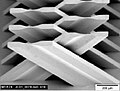
Gallery
[edit]Below is a gallery of LIGA-fabricated structures arranged by date.
-
![A nozzle for uranium enrichment.[1]](//upload.wikimedia.org/wikipedia/commons/thumb/e/e8/LIGA-Doppelumlenksystem.jpg/120px-LIGA-Doppelumlenksystem.jpg) A nozzle for uranium enrichment.[1]
A nozzle for uranium enrichment.[1] -
![A 517 μm tall copper coplanar waveguide.[3]](//upload.wikimedia.org/wikipedia/commons/thumb/b/b2/SNL-LIGA-CPW.jpg/120px-SNL-LIGA-CPW.jpg)
-
 Active part of a 2x2 optical switch, only the electrostatic actuator is shown.
 -
 Detail of the moulding tool for the LIGA microspectrometer.
 -
 X-ray refractive x-ray lenses made of SU8 polymer. The patterns are made by tilting the mask and substrate in the beam twice by +-45°.
![A 517 μm tall copper coplanar waveguide.[3]](https://en.wikipedia.org/wiki/File:SNL-LIGA-CPW.jpg)


Notes
[edit]- ^ a b Becker, E. W.; Ehrfeld, W.; Münchmeyer, D.; Betz, H.; Heuberger, A.; Pongratz, S.; Glashauser, W.; Michel, H. J.; Siemens, R. (1982). "Production of Separation-Nozzle Systems for Uranium Enrichment by a Combination of X-Ray Lithography and Galvanoplastics". Naturwissenschaften. 69 (11): 520–523. Bibcode:1982NW.....69..520B. doi:10.1007/BF00463495. S2CID 44245091.
- ^ "Electroforming process". Retrieved 12 November 2018.
- ^ Forman, Michael A. (2006). "Low-loss LIGA-fabricated coplanar waveguide and filter". 2006 Asia-Pacific Microwave Conference. pp. 1905–1907. doi:10.1109/APMC.2006.4429780. ISBN 978-4-902339-08-6. S2CID 44220821.
See also
[edit]References
[edit]- Madou, M. (2003). Fundamentals of Microfabrication. CRC. ISBN 978-0849308260.
- Saile, V. (2009). LIGA and its Applications. Wiley-VCH. ISBN 978-3-527-31698-4.
External links
[edit]Introduction
Definition and Principles
LIGA is a microfabrication technology derived from the German acronym for Lithographie (lithography), Galvanoformung (electroforming or electroplating), and Abformung (molding or replication).[4] This process enables the production of high-precision three-dimensional microstructures by integrating deep lithography for pattern definition, electroplating for structural material deposition, and molding for scalable replication.[5] The technique is particularly noted for its ability to create structures with exceptionally high aspect ratios, often exceeding 100:1 and reaching up to 1000:1 or more, allowing for tall, narrow features that are challenging to achieve with conventional methods.[6] At its core, LIGA begins with the exposure of a radiation-sensitive resist material on a substrate to transfer a high-resolution pattern, followed by selective removal of exposed or unexposed regions to form a mold cavity. Electroplating then fills this cavity with a conductive material, such as a metal, to create a durable master structure. Subsequent molding steps, including injection or reaction molding, allow for the mass production of identical copies in various materials.[7] This workflow supports feature sizes ranging from sub-micrometer lateral dimensions to millimeter-scale heights, providing versatility for complex geometries.[7] The resulting microstructures serve as components in microsystems, such as microelectromechanical systems (MEMS), sensors, and fluidic devices, with compatibility across metals, polymers, ceramics, and composites.[8] By emphasizing precision and reproducibility, LIGA facilitates the transition from prototype to high-volume manufacturing while maintaining structural integrity in demanding applications.[4]Historical Development
The LIGA process was invented in 1982 by a team led by Erwin Willy Becker and Wolfgang Ehrfeld at the Karlsruhe Nuclear Research Center (now Karlsruhe Institute of Technology) in Germany, initially aimed at producing high-aspect-ratio microstructures for nuclear applications such as uranium enrichment nozzles using synchrotron radiation-based X-ray lithography combined with electroplating and molding.[9] This seminal work, detailed in the first publication on the technique that year, marked a departure from traditional silicon micromachining by enabling the fabrication of tall, precise three-dimensional structures from a wide range of materials.[4] In the early 1980s, initial demonstrations of the process occurred at synchrotron facilities, including the ELSA storage ring at Bonn University, where it was used to create prototypes with aspect ratios exceeding 10:1, paving the way for applications in micro-optics such as refractive lenses and gratings.[10] These efforts highlighted LIGA's potential for producing components with sub-micrometer lateral resolution and heights up to several millimeters, far surpassing conventional photolithography limits at the time.[11] The 1990s saw significant expansion with the development of UV-LIGA to address the high costs of synchrotron access, incorporating UV-sensitive photoresists like polyimides and later SU-8 for thicker structures without specialized radiation sources.[9] Research centers such as IMTEK at the University of Freiburg advanced the technology through interdisciplinary MEMS projects, while commercialization gained traction in Europe via institutes like the Institut für Mikrostrukturtechnik (IMM) and in the USA through facilities like the Center for X-ray Lithography at the University of Wisconsin, leading to initial industrial production of microfluidic and sensor components.[12] From the 2000s onward, LIGA integrated deeply with MEMS ecosystems, exemplified by collaborations between European developers and Sandia National Laboratories in the USA.[13] Post-2010 adaptations have extended LIGA to nanomaterials and hybrid processes. As of 2023, recent developments include digital LIGA, which integrates droplet-on-demand inkjet printing with electrodeposition to fabricate complex 3D mechanical structures, enhancing scalability for applications in photonics and biotechnology.[14] This evolution has established LIGA as a cornerstone for high-precision, non-silicon manufacturing, influencing fields requiring durable, high-aspect-ratio components.Process Variants
X-ray LIGA
X-ray LIGA, the foundational variant of the LIGA process, utilizes synchrotron-generated X-rays with wavelengths typically in the range of 0.5-5 nm to achieve deep penetration into thick photoresists, enabling exposure of layers up to 1 mm in thickness.[15] These soft X-rays, produced at dedicated beamlines, provide the high flux and parallelism necessary for precise patterning in high-aspect-ratio microstructures. The process relies on X-ray lithography where a mask aligned above the resist allows selective exposure, cross-linking the polymer in illuminated areas while leaving shadowed regions intact for subsequent development.[6] A primary advantage of X-ray LIGA is its capability to produce sub-micron lateral resolution alongside aspect ratios exceeding 100:1, attributed to the parallel beam collimation of synchrotron radiation and the minimal diffraction effects at these short wavelengths.[16] This results in vertical sidewalls with run-out errors less than 0.1 µm per 100 µm of resist thickness, far surpassing conventional lithographic techniques.[6] Polymethyl methacrylate (PMMA) serves as the standard resist material due to its high contrast and suitability for thick films, with a sensitivity of approximately 100 mJ/cm² under optimized conditions.[16] Exposures are conducted at synchrotron facilities such as ANKA in Germany or the National Synchrotron Light Source (NSLS) in the United States, where monochromatic, high-flux X-rays are filtered to match the desired energy spectrum, typically requiring times ranging from minutes to hours depending on resist thickness and beam intensity.[16] Despite its precision, X-ray LIGA faces unique limitations stemming from the reliance on synchrotron sources, including high operational costs—often exceeding 500 € per hour of beam time as of 2025—and restricted access due to limited global facilities and scheduling demands.[16][17][18] Beamline setups must provide stable, monochromatic radiation with fluxes exceeding 10^{12} photons/s/mm² to ensure uniform exposure, further complicating scalability for routine production.[6] Early applications demonstrated the process's potential in fabricating precision components, such as micron-scale nozzles for uranium enrichment systems and fine gears with 5 µm tooth widths, highlighting its role in prototyping high-performance microstructures.[16][6]UV-LIGA
UV-LIGA represents an adaptation of the LIGA process that substitutes ultraviolet (UV) radiation for X-ray exposure, facilitating high-aspect-ratio microstructures in settings without access to synchrotron facilities. This variant prioritizes cost-effectiveness and scalability by leveraging standard laboratory equipment, such as mask aligners, to pattern thick photoresists on substrates. Developed primarily in the mid-1990s, UV-LIGA gained prominence through the introduction of SU-8, an epoxy-based negative-tone photoresist formulated by IBM researchers and commercialized by MicroChem Corporation around 1997, enabling the fabrication of molds for electroplating without the infrastructure demands of X-ray methods. Often termed "poor man's LIGA," it emerged as a practical alternative for industrial prototyping and production, with early demonstrations focusing on microstructures up to several hundred micrometers in height.[9] The radiation source in UV-LIGA typically consists of UV lamps, such as mercury arc or mercury-xenon lamps, emitting in the near-UV spectrum of 350-400 nm, with primary activation at the i-line wavelength of 365 nm. These sources support tabletop setups, contrasting sharply with the synchrotron requirements of X-ray LIGA, and deliver sufficient intensity for exposing thick resist layers in compact environments. A hallmark feature is the use of SU-8 photoresist, which can achieve thicknesses up to 500 µm and support aspect ratios of 10-50:1, far exceeding conventional UV lithography limits. Exposure occurs via contact or proximity lithography, where the mask is placed directly or with a minimal gap on the resist-coated substrate to transfer patterns into the material. The photoresist's sensitivity, exemplified by doses around 90-200 mJ/cm² for 200-500 µm layers depending on formulation and equipment, allows for efficient crosslinking without excessive energy input.[19][20][21] Process adaptations in UV-LIGA emphasize practicality over ultra-high precision, with exposure times reduced to seconds to minutes—typically 10-60 seconds for thinner layers and up to several minutes for thicker ones—facilitated by the higher photon flux of UV lamps compared to collimated X-rays. Alignment during exposure presents challenges from diffraction at longer UV wavelengths, which can blur features in proximity setups; this is addressed through proximity masks maintaining gaps of 20-50 µm to minimize contact-induced defects while controlling edge acuity. Post-exposure baking and development follow standard SU-8 protocols to solidify patterns, enabling subsequent electroplating steps akin to the core LIGA sequence. These modifications enhance throughput, allowing batch processing in standard cleanrooms.[22][21][23] Despite its advantages, UV-LIGA involves trade-offs, including reduced resolution of approximately 5-10 µm laterally due to diffraction and scattering in thick resists, in contrast to the sub-micrometer capabilities of X-ray LIGA. However, this is offset by markedly higher throughput and lower operational costs, as the process avoids synchrotron scheduling and enables on-site replication for applications requiring moderate precision at scale. Seminal contributions, such as the 1997 IBM work on SU-8 for high-aspect-ratio molding, underscore its role in democratizing LIGA technology for widespread adoption in microsystems fabrication.[24][9]Advanced Variants
Advanced variants of the LIGA process extend its capabilities beyond traditional X-ray and UV lithography by integrating complementary techniques to address limitations in material compatibility, structural complexity, and feature resolution. These modifications enable the fabrication of microstructures in challenging materials and geometries, particularly for applications requiring three-dimensionality or release mechanisms.[25] LIGA-EDM combines LIGA-fabricated electrodes with micro-electro-discharge machining (micro-EDM) to process hard materials such as titanium, stainless steel, and tungsten carbide-cobalt composites that are difficult to electroform directly. In this approach, high-aspect-ratio nickel electrodes are produced via LIGA and then used to erode complementary microstructures in the target material through spark erosion, allowing the creation of complex 3D shapes with aspect ratios exceeding 10:1 and tolerances below 5 μm. This variant improves material compatibility, including for shape memory alloys like nickel-titanium (NiTi), by enabling post-molding machining that avoids the internal stresses associated with direct electroplating of such alloys.[26][25][27] SLIGA, or Sacrificial LIGA, incorporates sacrificial layers—typically polymers like polymethyl methacrylate (PMMA)—between the substrate and electroformed metal to produce multilayer structures and freestanding, released components. After electroplating and molding, the sacrificial layer is selectively dissolved, yielding movable microstructures such as cantilevers or gears for microelectromechanical systems (MEMS) sensors, with heights up to several hundred micrometers and gaps as small as 10 μm. This technique is particularly suited for MEMS devices requiring mechanical freedom, as demonstrated in the fabrication of accelerometers and micromotors.[28][2] Other extensions include laser-based LIGA variants, which employ femtosecond lasers to generate curvilinear features like micro-threads in polymers or metals, achieving resolutions down to 1 μm without the need for synchrotron sources. Hybrid LIGA with nanoimprint lithography further refines sub-micron scales by combining LIGA molds with thermal or UV nanoimprinting, enabling high-aspect-ratio patterns (up to 28:1) in hybrid sol-gel materials for photonic or optical devices.[29][30] In the 2010s and 2020s, LIGA variants have integrated with additive manufacturing, such as using LIGA molds in 3D-printed meso-scale assemblies for scalable production of parts up to millimeters in size, enhancing throughput for biomedical applications like microfluidic molds. These developments also address persistent challenges, including residual stresses in electroforms—often exceeding 100 MPa in nickel deposits—which can cause warping; mitigation strategies involve pulse electroplating with additives like saccharin to reduce stress below 50 MPa while maintaining deposition rates of 10-20 μm/h. Such innovations have expanded LIGA's role in biotechnology, where hybrid molds facilitate precise replication of tissue scaffolds with feature sizes under 50 μm.[14][31][32]Core Process Steps
Mask Fabrication
In the LIGA process, masks function as the primary patterning elements during lithography, precisely defining the geometry of high-aspect-ratio microstructures in the photoresist while ensuring alignment tolerances below 1 µm between multiple exposure levels or replication steps.[33] These masks must exhibit superior dimensional stability and pattern fidelity to accommodate the demands of deep lithography, where even minor distortions can compromise the final structure's accuracy. For X-ray LIGA, absorber masks are employed, featuring a dense, high-atomic-number layer such as gold or tungsten (typically 20–50 µm thick) patterned atop a low-absorbing carrier membrane like beryllium (around 500 µm thick) or titanium (3–10 µm thick) to support the absorber while transmitting X-rays efficiently.[34] [35] Fabrication begins with electron-beam lithography to delineate high-resolution patterns directly on an intermediate resist-coated substrate, followed by electroplating or sputtering of the absorber material and selective etching to form the final structure, achieving resolutions as fine as 0.1 µm.[36] [37] These X-ray masks require high X-ray contrast for sharp pattern transfer and mechanical robustness to endure synchrotron radiation without deformation, with beryllium carriers particularly valued for their low thermal expansion.[38] However, exposure-induced heating can cause mask distortion, which is mitigated through active cooling mechanisms such as forced nitrogen convection to maintain pattern integrity.[39] Due to the intricate fabrication involving specialized lithography and materials handling, X-ray masks often exceed $10,000 in cost, limiting their use to high-value applications.[40] In UV-LIGA variants, simpler chrome-on-glass photomasks are utilized, where a thin chromium layer (approximately 0.1 µm) on a quartz or soda-lime glass substrate serves as the opaque pattern, offering sufficient contrast for ultraviolet exposure at lower costs than X-ray equivalents.[41] These masks are produced via standard photolithography or laser writing to transfer designs from CAD files, patterned through chrome etching and resist stripping, enabling resolutions suitable for aspect ratios up to 20:1 in thick SU-8 photoresists.[42]Substrate Preparation and Exposure
Substrate preparation in the LIGA process begins with selecting an appropriate base material to support the resist layer and subsequent electroplating steps. Common substrates include silicon wafers, often coated with a thin conductive layer such as 2 µm titanium followed by carbon for better adhesion and conductivity; glass for UV transparency in backside exposures; or metal foils like stainless steel or copper, typically with thicknesses ranging from 0.5 to 2 mm to ensure mechanical stability during handling and processing.[11] These substrates must be thoroughly cleaned to remove organic contaminants, particulates, and oxides that could compromise resist adhesion or pattern fidelity; standard methods involve sequential rinsing in solvents such as acetone, isopropyl alcohol, and deionized water, followed by drying with nitrogen gas, or alternatively, oxygen plasma treatment to activate the surface and enhance bonding.[43] A conductive seed layer, if not inherent to the substrate, is sputtered onto non-conductive materials like glass to enable later electroplating.[44] Following cleaning, the photoresist is applied to form a thick, uniform layer critical for achieving high-aspect-ratio structures. In X-ray LIGA, polymethyl methacrylate (PMMA) is the predominant resist, applied either by spin-coating a liquid solution for layers up to several hundred micrometers or by lamination of prefabricated PMMA foils (100 µm to 1 mm thick) onto the substrate, sometimes followed by milling to precise thickness; a post-application bake at elevated temperatures (e.g., 180°C for PMMA) ensures solvent evaporation and strong adhesion.[11][44] For UV-LIGA variants, epoxy-based resists like SU-8 are favored for their compatibility with near-UV light, applied via multi-step spin-coating to achieve thicknesses from 100 µm to over 1 mm, with a soft bake (e.g., 65–95°C ramped to 95°C for 1–5 minutes per 100 µm) to remove solvents and promote planarization without cracking.[43] The mask, fabricated with high-contrast absorber patterns, is positioned over the resist-coated substrate to define the microstructures during irradiation.[11] The exposure step transfers the mask pattern into the resist through selective irradiation, exploiting differences in radiation sensitivity. In X-ray LIGA, synchrotron-generated hard X-rays (typically 0.5–5 keV) penetrate the resist in proximity (5–50 µm gap) or contact mode to minimize diffraction, with parallel beam geometry preferred for uniform illumination over large areas (up to 10 cm²); dosage is precisely controlled based on resist thickness and composition, often requiring an absorbed energy of approximately 5–6 kJ/cm³ in PMMA to achieve complete cross-linking without bubbling or swelling, corresponding to incident doses scaling from hundreds of mJ/cm² for thin layers to several kJ/cm² for millimeter-scale depths.[45] UV-LIGA employs collimated i-line (365 nm) or broadband UV sources in vacuum contact or proximity mode, with exposure doses ranging from 100–1000 mJ/cm² for thinner SU-8 layers up to 2000–5000 mJ/cm² for 300–500 µm thicknesses to ensure full depth penetration and sidewall steepness exceeding 90°.[43] Beam divergence is minimized using optics or pinholes, and exposure occurs in a scanned raster mode for uniform energy delivery across the substrate. For multi-layer LIGA structures, precise alignment between sequential exposures is essential to maintain feature registry, achieved through optical microscopy for UV processes or X-ray interferometry and fiducial markers for X-ray LIGA, enabling sub-micrometer accuracy over stacked layers up to several millimeters total height; throughput is influenced by scan speeds (typically 1–10 mm/s) and exposure times (minutes to hours), balancing dose uniformity with production efficiency.[11] Safety protocols are paramount, particularly for X-ray exposures requiring lead-lined shielding and remote operation to protect against ionizing radiation, while UV-LIGA often employs inert atmospheres (e.g., nitrogen purging) to mitigate oxygen inhibition of radical polymerization in thick SU-8 layers, preventing surface tackiness and incomplete cross-linking.[43]Development
The development step in the LIGA process involves the selective chemical dissolution of the exposed regions of the photoresist to form the mold cavity, revealing the patterned microstructure with high fidelity. For polymethyl methacrylate (PMMA), a positive-tone resist commonly used in X-ray LIGA, wet chemical development employs the GG developer, a mixture composed of 60 vol.% 2-(2-butoxyethoxy)ethanol, 20 vol.% γ-butyrolactone, 15 vol.% morpholine, and 5 vol.% ethanolamine.[46] This solvent-based etchant targets the chain-scissioned polymer chains in exposed areas, achieving isotropic dissolution while preserving unexposed regions. In UV-LIGA variants using SU-8, a negative-tone epoxy-based resist, development utilizes propylene glycol monomethyl ether acetate (PGMEA) to remove unexposed material, leveraging the cross-linked nature of exposed areas for structural integrity. Dry plasma methods, such as oxygen reactive ion etching, may supplement wet development for precision trimming in specialized cases, offering anisotropic control to refine sidewalls without significant lateral erosion.[47] Process parameters are critical to maintain high aspect ratios and minimize defects during development. Typical temperatures range from 20°C to 60°C, with higher values accelerating dissolution rates but risking thermal stress in thick resists (>500 μm).[48] Agitation, often via ultrasonic or acoustic methods at frequencies around 1 MHz and power densities up to 6 W/cm², ensures uniform developer access and reduces development times from hours to potentially less than one hour for structures with aspect ratios of 10:1 or higher, by enhancing mass transport up to 4-6 times over diffusion alone.[48] Selectivity exceeds 100:1 between exposed and unexposed regions in PMMA, enabling dissolution rates of about 10 μm/min in irradiated areas while unexposed PMMA remains largely intact over extended periods.[49] For SU-8, PGMEA development similarly yields selectivities >100:1, with times scaling to several hours for thicknesses beyond 500 μm, controlled by post-exposure bake conditions to optimize cross-linking. Post-development inspection focuses on sidewall quality to verify mold integrity, using scanning electron microscopy (SEM) for detailed profiling or optical microscopy for initial assessment. Achievable sidewall roughness is typically below 50 nm RMS, contributing to smooth replication in subsequent steps.[50] Common defects include undercutting at the base of high-aspect-ratio features, which can be mitigated by exposure techniques that minimize diffraction effects, such as using synchrotron sources with collimated beams.[48] Careful control of developer concentration and periodic rinsing further preserves aspect ratios up to 100:1 without significant taper or swelling.[51]Electroplating
In the electroplating step of the LIGA process, the developed resist mold on a conductive substrate serves as the cathode, which is immersed in an electrolyte bath alongside an anode typically made of the same metal to facilitate electrodeposition into the mold voids. For nickel deposition, a common sulfamate-based electrolyte is used, containing 76–90 g/L nickel ions, 40 g/L boric acid as a pH buffer, and wetting agents (e.g., 10 mL/L sodium lauryl sulfate) to ensure complete mold wetting and prevent gas bubble adhesion.[52] The bath is maintained at a pH of 3.5–4.0 and temperature of 50–62°C to optimize deposition efficiency and minimize side reactions.[52] A direct current is applied with typical densities of 10–100 mA/cm² (1–10 A/dm²), controlled to balance deposition rate and structural integrity.[52] The growth mechanics involve the reduction of metal ions at the cathode surface, such as Ni²⁺ + 2e⁻ → Ni for nickel, occurring preferentially within the high-aspect-ratio mold features to build the microstructure from the bottom up. Deposition rates for nickel typically range from 10–50 µm/h, depending on current density and bath conditions, with lower rates (e.g., ~12 µm/h at 10 mA/cm²) favoring uniform filling in deep molds.[52][53] Pulse plating techniques enhance uniformity by alternating high-current pulses (e.g., current density i_p, duration t_d) with off periods (pause t_p), calculated as average current i_a = (t_d / (t_d + t_p)) × i_p, which reduces internal stresses, grain size, and porosity compared to direct current methods.[52] Common metals include nickel for its mechanical strength, copper for conductivity, and gold for corrosion resistance, while alloys like Ni-Fe (permalloy) are selected for magnetic applications in sensors.[52] Quality control measures address challenges such as hydrogen evolution during plating, which can cause embrittlement; this is mitigated by post-plating baking at ~200°C for several hours to diffuse out absorbed hydrogen.[54] Thickness uniformity is achieved through bath agitation to renew electrolyte at the cathode and prevent concentration gradients in high-aspect-ratio features (>10:1).[52] Overplating beyond the mold height ensures complete void filling, particularly at the mold bottom, followed by mechanical finishing if needed. Yields exceed 95% for well-controlled high-aspect-ratio molds when using filtered electrolytes and optimized parameters to minimize defects like voids or incomplete wetting.[52][55]Molding and Replication
After electroplating, the remaining resist, such as polymethyl methacrylate (PMMA), is stripped to free the metal master structure, typically using chemical solvents like acetone or oxygen plasma ashing for uncross-linked portions, while cross-linked PMMA may require additional synchrotron radiation exposure to enhance solubility before dissolution.[52][56] Mechanical methods can also be employed for removal if chemical approaches are insufficient.[52] The freed electroplated metal master, often nickel, serves as a mold insert for replication via techniques such as injection molding or hot embossing to produce multiple polymer copies. Injection molding involves injecting molten thermoplastics like PMMA or polycarbonate (PC) into the mold cavity under high pressure, followed by cooling to solidify the structure.[52] Hot embossing, alternatively, heats the polymer sheet above its glass transition temperature and presses it against the mold under vacuum conditions before cooling and demolding.[52] These methods operate at pressures ranging from 100 to 1000 bar and temperatures of 150 to 300°C, depending on the polymer, to ensure proper flow and filling of high-aspect-ratio features.[52] Replication fidelity in these processes achieves dimensional accuracy of ±1-5 µm, preserving the high-aspect-ratio microstructures from the master, with injection molding cycle times on the order of seconds for efficient production.[52] This enables scaling to thousands of copies from a single master, enhancing cost-effectiveness for batch fabrication.[52] Variants, such as using micro-electro-discharge machining (micro-EDM) to create or refine metal molds, further support replication in metallic materials when polymer copies are insufficient.[52] Post-processing of replicated parts includes trimming excess material and assembly into functional components, often with techniques like reactive ion etching to remove residual layers.[52] Nickel molds demonstrate robust durability, supporting over 10^6 replication cycles without significant degradation.[52]Materials and Equipment
Key Materials
The LIGA process relies on a selection of specialized materials tailored to its high-aspect-ratio fabrication demands, including photoresists for lithography, metals for electroplating, and substrates for structural support and replication. These materials are chosen for their radiation sensitivity, mechanical properties, and compatibility with subsequent process steps, ensuring precise patterning and durable microstructures.[57]Photoresists
Photoresists form the core of the lithography phase in LIGA, providing high-resolution patterning for thick films up to several millimeters. Polymethyl methacrylate (PMMA) is a positive-tone, radiation-sensitive resist widely used in X-ray LIGA due to its high spatial resolution and low-roughness sidewalls, enabling aspect ratios exceeding 100:1 in microstructures. PMMA exhibits excellent mechanical strength and thermal stability, with a glass transition temperature (Tg) of approximately 105°C, making it suitable for processes involving elevated temperatures without deformation. Its high transparency to visible light facilitates alignment during fabrication, though it requires longer exposure times owing to lower photosensitivity compared to alternatives. Selection criteria for PMMA emphasize its cost-effectiveness for large-scale production, though specific pricing varies by supplier and grade.[57][58][57] SU-8, an epoxy-based negative-tone photoresist, is preferred in UV-LIGA variants for its superior chemical stability and ability to form thick, cross-linked structures resistant to solvents and mechanical stress. It offers high photosensitivity and contrast, supporting single-layer coatings from 1.5 µm to 500 µm thick with viscosities ranging from 2 cSt to 51,500 cSt, which allows precise control over film thickness for high-aspect-ratio features up to 100:1. SU-8's robust physical properties, including low shrinkage and high adhesion when properly processed, make it ideal for molds in electroplating, though internal stresses can pose challenges in very thick layers. Commercial suppliers such as Kayaku Advanced Materials (formerly MicroChem) provide SU-8 formulations optimized for MEMS applications, ensuring consistency in viscosity and sensitivity.[20][59][60]| Property | PMMA | SU-8 |
|---|---|---|
| Tone | Positive | Negative |
| Contrast Ratio | Moderate (lower sensitivity) | High (enables sharp sidewalls) |
| Thermal Stability (Tg) | ~105°C | >200°C (cross-linked) |
| Max Thickness | Up to mm-scale (cast) | 500 µm (single coat) |
| Key Advantage | High resolution, low cost | Chemical resistance, thick films |
Electroplating Metals
Electroplating in LIGA fills resist-patterned molds to create metallic microstructures, with metal selection based on mechanical, electrical, and environmental properties. Nickel is the most commonly used due to its high tensile strength (up to 500 MPa in electroplated form) and excellent corrosion resistance, providing durable components for harsh environments like sensors and actuators. Copper serves as an alternative for applications requiring high electrical conductivity (approximately 58 MS/m) and faster deposition rates, which reduce processing time in high-volume production. For biomedical uses, gold is selected for its superior biocompatibility and inertness, minimizing tissue reactions while maintaining good conductivity (44 MS/m), though its higher cost limits it to specialized devices. Compatibility with LIGA variants favors metals that adhere well to substrates without inducing stress cracks during plating.[62][63][62]Substrates and Molds
Substrates provide the foundation for resist application and must offer flatness, thermal compatibility, and ease of integration with electroplating bases. Silicon wafers are standard in X-ray and UV-LIGA for their exceptional surface flatness (sub-micron level) and compatibility with semiconductor processing tools, enabling precise alignment and minimal distortion during exposure. For replication in molding steps, polymers such as polycarbonate are favored for low-cost production of flexible, high-impact replicas; polycarbonate exhibits a density of 1.2 g/cm³, tensile strength of 60-70 MPa, and good optical transparency, allowing mass replication via hot embossing or injection molding. Selection criteria prioritize substrates that withstand development and plating without warping, with silicon suited for prototypes and polycarbonate for scalable, economical end-use parts. A simple compatibility matrix highlights material pairings:| Variant | Preferred Substrate | Key Compatibility Notes |
|---|---|---|
| X-ray LIGA | Silicon | High flatness for mask alignment |
| UV-LIGA | Silicon or Glass | UV transparency, thermal stability |
| Replication | Polycarbonate | Flexibility for demolding, low cost |