
Community hub
Recent from talks
Contribute something
Nothing was collected or created yet.
Sputter deposition
View on Wikipedia
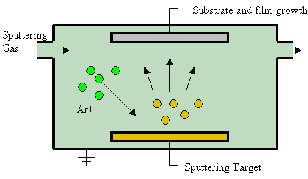
Sputter deposition is a physical vapor deposition (PVD) method of thin film deposition by the phenomenon of sputtering. This involves ejecting material from a "target" that is a source onto a "substrate" such as a silicon wafer.
Resputtering is re-emission of the deposited material during the deposition process by ion or atom bombardment.[1][2]
Sputtered atoms ejected from the target have a wide energy distribution, typically up to tens of eV (100,000 K). The sputtered ions (typically only a small fraction of the ejected particles are ionized — on the order of 1 percent) can ballistically fly from the target in straight lines and impact energetically on the substrates or vacuum chamber (causing resputtering). Alternatively, at higher gas pressures, the ions collide with the gas atoms that act as a moderator and move diffusively, reaching the substrates or vacuum chamber wall and condensing after undergoing a random walk. The entire range from high-energy ballistic impact to low-energy thermalized motion is accessible by changing the background gas pressure.
The sputtering gas is often an inert gas such as argon. For efficient momentum transfer, the atomic weight of the sputtering gas should be close to the atomic weight of the target, so for sputtering light elements neon is preferable, while for heavy elements krypton or xenon are used.[3] Reactive gases can also be used to sputter compounds.
The compound can be formed on the target surface, in-flight or on the substrate depending on the process parameters. The availability of many parameters that control sputter deposition make it a complex process, but also allow experts a large degree of control over the growth and microstructure of the film.
Uses
[edit]One of the earliest widespread commercial applications of sputter deposition, which is still one of its most important applications, is in the production of computer hard disks. Sputtering is used extensively in the semiconductor industry to deposit thin films of various materials in integrated circuit processing. Thin antireflection coatings on glass for optical applications are also deposited by sputtering. Because of the low substrate temperatures used, sputtering is an ideal method to deposit contact metals for thin-film transistors. Another familiar application of sputtering is low-emissivity coatings on glass, used in double-pane window assemblies. The coating is a multilayer containing silver and metal oxides such as zinc oxide, tin oxide, or titanium dioxide. A large industry has developed around tool bit coating using sputtered nitrides, such as titanium nitride, creating the familiar gold colored hard coat. Sputtering is also used as the process to deposit the metal (e.g., aluminium) layer during the fabrication of CDs and DVDs.
Hard disk surfaces use sputtered CrOx and other sputtered materials. Sputtering is one of the main processes of manufacturing optical waveguides and is another way for making efficient photovoltaic and thin film solar cells.[4][5]
In 2022, researchers at IMEC built up lab superconducting qubits with coherence times exceeding 100 μs and an average single-qubit gate fidelity of 99.94%, using CMOS-compatible fabrication techniques such as sputtering deposition and subtractive etch.[6]
Sputter coating
[edit]
Sputter coating in scanning electron microscopy is a sputter deposition process[clarification needed] to cover a specimen with a thin layer of conducting material, typically a metal, such as a gold/palladium (Au/Pd) alloy. A conductive coating is needed to prevent charging of a specimen with an electron beam in conventional SEM mode (high vacuum, high voltage). While metal coatings are also useful for increasing signal to noise ratio (heavy metals are good secondary electron emitters), they are of inferior quality when X-ray spectroscopy is employed. For this reason when using X-ray spectroscopy a carbon coating is preferred.[7]
Comparison with other deposition methods
[edit]
An important advantage of sputter deposition is that even materials with very high melting points are easily sputtered while evaporation of these materials in a resistance evaporator or Knudsen cell is problematic or impossible. Sputter deposited films have a composition close to that of the source material. The difference is due to different elements spreading differently because of their different mass (light elements are deflected more easily by the gas) but this difference is constant. Sputtered films typically have a better adhesion on the substrate than evaporated films. A target contains a large amount of material and is maintenance free making the technique suited for ultrahigh vacuum applications. Sputtering sources contain no hot parts (to avoid heating they are typically water cooled) and are compatible with reactive gases such as oxygen. Sputtering can be performed top-down while evaporation must be performed bottom-up. Advanced processes such as epitaxial growth are possible.
Some disadvantages of the sputtering process are that the process is more difficult to combine with a lift-off for structuring the film. This is because the diffuse transport, characteristic of sputtering, makes a full shadow impossible. Thus, one cannot fully restrict where the atoms go, which can lead to contamination problems. Also, active control for layer-by-layer growth is difficult compared to pulsed laser deposition and inert sputtering gases are built into the growing film as impurities. Pulsed laser deposition is a variant of the sputtering deposition technique in which a laser beam is used for sputtering. Role of the sputtered and resputtered ions and the background gas is fully investigated during the pulsed laser deposition process.[8][9]
Types of sputter deposition
[edit]
Sputtering sources often employ magnetrons that utilize strong electric and magnetic fields to confine charged plasma particles close to the surface of the sputter target. In a magnetic field, electrons follow helical paths around magnetic field lines, undergoing more ionizing collisions with gaseous neutrals near the target surface than would otherwise occur. (As the target material is depleted, a "racetrack" erosion profile may appear on the surface of the target.) The sputter gas is typically an inert gas such as argon. The extra argon ions created as a result of these collisions lead to a higher deposition rate. The plasma can also be sustained at a lower pressure this way. The sputtered atoms are neutrally charged and so are unaffected by the magnetic trap. Charge build-up on insulating targets can be avoided with the use of RF sputtering where the sign of the anode-cathode bias is varied at a high rate (commonly 13.56 MHz).[10] RF sputtering works well to produce highly insulating oxide films but with the added expense of RF power supplies and impedance matching networks. Stray magnetic fields leaking from ferromagnetic targets also disturb the sputtering process. Specially designed sputter guns with unusually strong permanent magnets must often be used in compensation.
Ion-beam sputtering
[edit]
Ion-beam sputtering (IBS) is a method in which the target is external to the ion source. A source can work without any magnetic field like in a hot filament ionization gauge. In a Kaufman source ions are generated by collisions with electrons that are confined by a magnetic field as in a magnetron. They are then accelerated by the electric field emanating from a grid toward a target. As the ions leave the source they are neutralized by electrons from a second external filament. IBS has an advantage in that the energy and flux of ions can be controlled independently. Since the flux that strikes the target is composed of neutral atoms, either insulating or conducting targets can be sputtered. IBS has found application in the manufacture of thin-film heads for disk drives. A pressure gradient between the ion source and the sample chamber is generated by placing the gas inlet at the source and shooting through a tube into the sample chamber. This saves gas and reduces contamination in UHV applications. The principal drawback of IBS is the large amount of maintenance required to keep the ion source operating.[11]
Reactive sputtering
[edit]In reactive sputtering, the sputtered particles from a target material undergo a chemical reaction aiming to deposit a film with different composition on a certain substrate. The chemical reaction that the particles undergo is with a reactive gas introduced into the sputtering chamber such as oxygen or nitrogen, enabling the production of oxide and nitride films, respectively.[12] The introduction of an additional element to the process, i.e. the reactive gas, has a significant influence in the desired depositions, making it more difficult to find ideal working points. Like so, the wide majority of reactive-based sputtering processes are characterized by an hysteresis-like behavior, thus needing proper control of the involved parameters, e.g. the partial pressure of working (or inert) and reactive gases, to undermine it.[13] Berg et al. proposed a significant model, i.e. Berg Model, to estimate the impact upon addition of the reactive gas in sputtering processes. Generally, the influence of the reactive gas' relative pressure and flow were estimated in accordance to the target's erosion and film's deposition rate on the desired substrate.[14] The composition of the film can be controlled by varying the relative pressures of the inert and reactive gases. Film stoichiometry is an important parameter for optimizing functional properties like the stress in SiNx and the index of refraction of SiOx.
Ion-assisted deposition
[edit]In ion-assisted deposition (IAD), the substrate is exposed to a secondary ion beam operating at a lower power than the sputter gun. Usually a Kaufman source, like that used in IBS, supplies the secondary beam. IAD can be used to deposit carbon in diamond-like form on a substrate. Any carbon atoms landing on the substrate which fail to bond properly in the diamond crystal lattice will be knocked off by the secondary beam. NASA used this technique to experiment with depositing diamond films on turbine blades in the 1980s. IAD is used in other important industrial applications such as creating tetrahedral amorphous carbon surface coatings on hard disk platters and hard transition metal nitride coatings on medical implants.

High-target-utilisation sputtering (HiTUS)
[edit]Sputtering may also be performed by remote generation of a high density plasma. The plasma is generated in a side chamber opening into the main process chamber, containing the target and the substrate to be coated. As the plasma is generated remotely, and not from the target itself (as in conventional magnetron sputtering), the ion current to the target is independent of the voltage applied to the target.
High-power impulse magnetron sputtering (HiPIMS)
[edit]HiPIMS is a method for physical vapor deposition of thin films which is based on magnetron sputter deposition. HiPIMS utilizes extremely high power densities of the order of kW/cm2 in short pulses (impulses) of tens of microseconds at low duty cycle of < 10%.
Gas flow sputtering
[edit]Gas flow sputtering makes use of the hollow cathode effect, the same effect by which hollow cathode lamps operate. In gas flow sputtering a working gas like argon is led through an opening in a metal subjected to a negative electrical potential.[15][16] Enhanced plasma densities occur in the hollow cathode, if the pressure in the chamber p and a characteristic dimension L of the hollow cathode obey the Paschen's law 0.5 Pa·m < p·L < 5 Pa·m. This causes a high flux of ions on the surrounding surfaces and a large sputter effect. The hollow-cathode based gas flow sputtering may thus be associated with large deposition rates up to values of a few μm/min.[17]
Structure and morphology
[edit]In 1974 J. A. Thornton applied the structure zone model for the description of thin film morphologies to sputter deposition. In a study on metallic layers prepared by DC sputtering,[18] he extended the structure zone concept initially introduced by Movchan and Demchishin for evaporated films.[19] Thornton introduced a further structure zone T, which was observed at low argon pressures and characterized by densely packed fibrous grains. The most important point of this extension was to emphasize the pressure p as a decisive process parameter. In particular, if hyperthermal techniques like sputtering etc. are used for the sublimation of source atoms, the pressure governs via the mean free path the energy distribution with which they impinge on the surface of the growing film. Next to the deposition temperature Td the chamber pressure or mean free path should thus always be specified when considering a deposition process.
Since sputter deposition belongs to the group of plasma-assisted processes, next to neutral atoms also charged species (like argon ions) hit the surface of the growing film, and this component may exert a large effect. Denoting the fluxes of the arriving ions and atoms by Ji and Ja, it turned out that the magnitude of the Ji/Ja ratio plays a decisive role on the microstructure and morphology obtained in the film.[20] The effect of ion bombardment may quantitatively be derived from structural parameters like preferred orientation of crystallites or texture and from the state of residual stress. It has been shown recently [21] that textures and residual stresses may arise in gas-flow sputtered Ti layers that compare to those obtained in macroscopic Ti work pieces subjected to a severe plastic deformation by shot peening.
See also
[edit]References
[edit]- ^ Gregoire, J. M.; Lobovsky, M. B.; Heinz, M. F.; DiSalvo, F. J.; van Dover, R. B. (26 November 2007). "Resputtering phenomena and determination of composition in codeposited films". Physical Review B. 76 (19) 195437. Bibcode:2007PhRvB..76s5437G. doi:10.1103/PhysRevB.76.195437.
- ^ Kester, Daniel J.; Messier, Russell (1 August 1993). "Macro-effects of resputtering due to negative ion bombardment of growing thin films". Journal of Materials Research. 8 (8): 1928–1937. Bibcode:1993JMatR...8.1928K. doi:10.1557/JMR.1993.1928. ISSN 2044-5326. S2CID 221977398.
- ^ Tong, Xingcun Colin (2014). PhD. Schaumburg, IL: Springer International Publishing. p. 42. ISBN 978-3-319-01549-1.
- ^ Green, Julissa (Apr 23, 2024). "An Overview of Sputtering Deposition". Sputter Targets. Retrieved Aug 1, 2024.
- ^ Vilcot, J.P.; Ayachi, B. (2017). "Full Sputtering Deposition of Thin Film Solar Cells: A Way of Achieving High Efficiency Sustainable Tandem Cells?". Journal of Electronic Materials. 46: 6523–6527. doi:10.1007/s11664-017-5694-3.
- ^ "High-quality superconducting qubits fabricated with CMOS-compatible technologies". August 19, 2022.
- ^ Newbery, Dale.; et al. (1986). Advanced Scanning Electron Microscopy and X-Ray Microanalysis. Plenum Press. ISBN 978-0-306-42140-2.
- ^ Rashidian Vaziri, M R; et al. (2010). "Microscopic description of the thermalization process during pulsed laser deposition of aluminium in the presence of argon background gas". Journal of Physics D: Applied Physics. 43 (42) 425205. Bibcode:2010JPhD...43P5205R. doi:10.1088/0022-3727/43/42/425205. S2CID 120309363.
- ^ Rashidian Vaziri, M R; et al. (2011). "Monte Carlo simulation of the subsurface growth mode during pulsed laser deposition". Journal of Applied Physics. 110 (4): 043304–043304–12. Bibcode:2011JAP...110d3304R. doi:10.1063/1.3624768.
- ^ Ohring, Milton. Materials Science of Thin Films (2nd ed.). Academic Press. p. 215.
- ^ Bernhard Wolf (1995). Handbook of ion sources. CRC Press. p. 222. ISBN 978-0-8493-2502-1.
- ^ Safi, I. (2000-05-22). "Recent aspects concerning DC reactive magnetron sputtering of thin films: a review". Surface and Coatings Technology. 127 (2): 203–218. doi:10.1016/S0257-8972(00)00566-1. ISSN 0257-8972.
- ^ Sproul, W. D.; Christie, D. J.; Carter, D. C. (2005-11-22). "Control of reactive sputtering processes". Thin Solid Films. 491 (1): 1–17. Bibcode:2005TSF...491....1S. doi:10.1016/j.tsf.2005.05.022. ISSN 0040-6090.
- ^ Berg, S.; Nyberg, T. (2005-04-08). "Fundamental understanding and modeling of reactive sputtering processes". Thin Solid Films. 476 (2): 215–230. Bibcode:2005TSF...476..215B. doi:10.1016/j.tsf.2004.10.051. ISSN 0040-6090.
- ^ K. Ishii (1989). "High-rate low kinetic energy gas-flow-sputtering system". Journal of Vacuum Science and Technology A. 7 (2): 256–258. Bibcode:1989JVSTA...7..256I. doi:10.1116/1.576129.
- ^ T. Jung & A. Westphal (1991). "Zirconia thin film deposition on silicon by reactive gas flow sputtering: the influence of low energy particle bombardment". Mater. Sci. Eng. A. 140: 528–533. doi:10.1016/0921-5093(91)90474-2.
- ^ K. Ortner; M. Birkholz & T. Jung (2003). "Neue Entwicklungen beim Hohlkatoden-Gasflusssputtern" (PDF). Vac. Praxis (in German). 15 (5): 236–239. doi:10.1002/vipr.200300196. S2CID 108638584.
- ^ J.A. Thornton (1974). "Influence of apparatus geometry and deposition conditions on the structure and topography of thick sputtered coatings". Journal of Vacuum Science and Technology. 11 (4): 666–670. Bibcode:1974JVST...11..666T. doi:10.1116/1.1312732.
- ^ B. A. Movchan & A. V. Demchishin (1969). "Study of the structure and properties of thick vacuum condensates of nickel, titanium, tungsten, aluminium oxide and zirconium dioxide". Phys. Met. Metallogr. 28: 83–90.
- ^ H. Windischman (1992). "Intrinsic stress in sputter-deposited thin film". Crit. Rev. Sol. St. Mat. Sci. 17 (6): 547–596. Bibcode:1992CRSSM..17..547W. doi:10.1080/10408439208244586. S2CID 94349281.
- ^ M. Birkholz; C. Genzel & T. Jung (2004). "X-ray diffraction study of residual stress and preferred orientation in thin titanium films subjected to a high ion flux during deposition" (PDF). J. Appl. Phys. 96 (12): 7202–7211. Bibcode:2004JAP....96.7202B. doi:10.1063/1.1814413.
Further reading
[edit]- The Foundations of Vacuum Coating Technology by D. Mattox
- William D. Westwood (2003). Sputter Deposition, AVS Education Committee Book Series. Vol. 2. ISBN 978-0-7354-0105-1.
- Kiyotaka Wasa & Shigeru Hayakawa (1992). Handbook of sputter deposition technology principles, technology and applications. Noyes Publications. ISBN 0-8155-1280-5.