Hubbry Logo
Optical rectennaOptical rectennaMain
Open search
Optical rectenna
Community hub
Optical rectenna
logo
8 pages, 0 posts
0 subscribers
Be the first to start a discussion here.
Optical rectenna
Optical rectenna
from Wikipedia
Figure 1. Spectral irradiance of wavelengths in the solar spectrum. The red shaded area shows the irradiance at sea level. There is less irradiance at sea level due to absorption of light by the atmosphere.

An optical rectenna is a rectenna (rectifying antenna) that works with visible or infrared light.[1] A rectenna is a circuit containing an antenna and a diode, which turns electromagnetic waves into direct current electricity. While rectennas have long been used for radio waves or microwaves, an optical rectenna would operate the same way but with infrared or visible light, turning it into electricity.

While traditional (radio- and microwave) rectennas are fundamentally similar to optical rectennas, it is vastly more challenging in practice to make an optical rectenna. One challenge is that light has such a high frequency—hundreds of terahertz for visible light—that only a few types of specialized diodes can switch quickly enough to rectify it. Another challenge is that antennas tend to be a similar size to a wavelength, so a very tiny optical antenna requires a challenging nanotechnology fabrication process. A third challenge is that, being very small, an optical antenna typically absorbs very little power, and therefore tend to produce a tiny voltage in the diode, which leads to low diode nonlinearity and hence low efficiency. Due to these and other challenges, optical rectennas have so far been restricted to laboratory demonstrations, typically with intense focused laser light producing a tiny but measurable amount of power.

Nevertheless, it is hoped that arrays of optical rectennas could eventually be an efficient means of converting sunlight into electric power, producing solar power more efficiently than conventional solar cells. The idea was first proposed by Robert L. Bailey in 1972.[2] As of 2012, only a few optical rectenna devices have been built, demonstrating only that energy conversion is possible.[3] It is unknown if they will ever be as cost-effective or efficient as conventional photovoltaic cells.

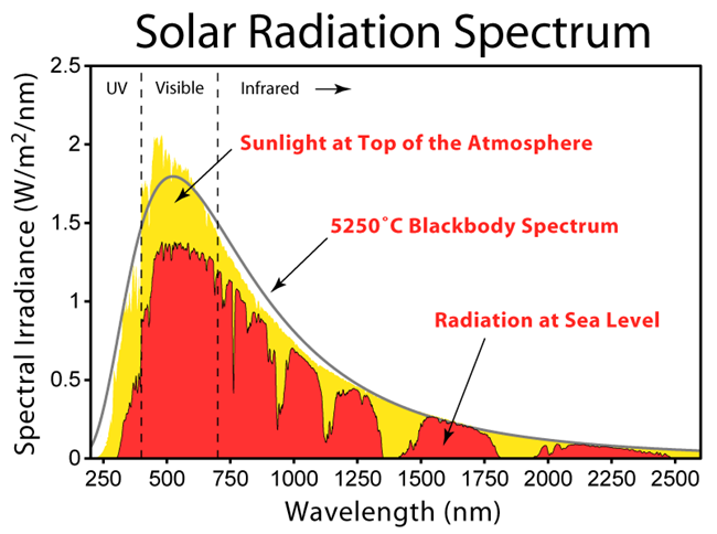
The term nantenna (nano-antenna) is sometimes used to refer to either an optical rectenna, or an optical antenna by itself. [4] In 2008 it was reported that Idaho National Laboratories designed an optical antenna to absorb wavelengths in the range of 3–15 μm.[5] These wavelengths correspond to photon energies of 0.4 eV down to 0.08 eV. Based on antenna theory, an optical antenna can absorb any wavelength of light efficiently provided that the size of the antenna is optimized for that specific wavelength. Ideally, antennas would be used to absorb light at wavelengths between 0.4 and 1.6 μm because these wavelengths have higher energy than far-infrared (longer wavelengths) and make up about 85% of the solar radiation spectrum[6] (see Figure 1).

History

[edit]

Robert Bailey, along with James C. Fletcher, received a patent (US 3760257 ) in 1973 for an "electromagnetic wave energy converter". The patented device was similar to modern day optical rectennas. The patent discusses the use of a diode "type described by [Ali Javan] in the IEEE Spectrum, October, 1971, page 91", to whit, a 100 nm-diameter metal cat's whisker to a metal surface covered with a thin oxide layer. Javan was reported as having rectified 58 THz infrared light. In 1974, T. Gustafson and coauthors demonstrated that these types of devices could rectify even visible light to DC current[7] Alvin M. Marks received a patent in 1984 for a device explicitly stating the use of sub-micron antennas for the direct conversion of light power to electrical power.[8] Marks's device showed substantial improvements in efficiency over Bailey's device.[9] In 1996, Guang H. Lin reported resonant light absorption by a fabricated nanostructure and rectification of light with frequencies in the visible range.[9] In 2002, ITN Energy Systems, Inc. published a report on their work on optical antennas coupled with high frequency diodes. ITN set out to build an optical rectenna array with single digit efficiency. Although they were unsuccessful, the issues associated with building a high efficiency optical rectenna were better understood.[6]

In 2015, Baratunde A. Cola's research team at the Georgia Institute of Technology, developed a solar energy collector that can convert optical light to DC current, an optical rectenna using carbon nanotubes,.[10] Vertical arrays of multiwall carbon nanotubes (MWCNTs) grown on a metal-coated substrates were coated with insulating aluminum oxide and altogether capped with a metal electrode layer. The small dimensions of the nanotubes act as antennae, capable of capturing optical wavelengths. The MWCNT also doubles as one layer of a metal-insulator-metal (MIM) tunneling diode. Due to the small diameter of MWCNT tips, this combination forms a diode that is capable of rectifying the high frequency optical radiation. The overall achieved conversion efficiency of this device is around 10−5 %.[10] Nonetheless, optical rectenna research is ongoing.

The primary drawback of these carbon nanotube rectenna devices is a lack of air stability. The device structure originally reported by Cola used calcium as a semitransparent top electrode because the low work function of calcium (2.9 eV) relative to MWCNTs (~5 eV) creates the diode asymmetry needed for optical rectification. However, metallic calcium is highly unstable in air and oxidizes rapidly. Measurements had to be made within a glovebox under an inert environment to prevent device breakdown. This limited practical application of the devices.

Cola and his team later solved the challenges with device instability by modifying the diode structure with multiple layers of oxide. In 2018 they reported the first air-stable optical rectenna along with efficiency improvements.

The air-stability of this new generation of rectenna was achieved by tailoring the diode's quantum tunneling barrier. Instead of a single dielectric insulator, they showed that the use of multiple dissimilar oxide layers enhances diode performance by modifying diode tunneling barrier. By using oxides with different electron affinities, the electron tunneling can be engineered to produce an asymmetric diode response regardless of the work function of the two electrodes. By using layers of Al2O3 and HfO2, a double-insulator diode (metal-insulator-insulator-metal (MIIM)) was constructed that improved the diode's asymmetric response more than 10-fold without the need for low work function calcium, and the top metal was subsequently replaced with air-stable silver.

Future efforts will be focused on improving the device efficiency by investigating alternative materials, manipulating the MWCNTs and the insulating layers to encourage conduction at the interface, and reduce resistances within the structure.

Another approach was presented in 2022 by Proietti Zaccaria Remo and collaborators at the Italian Institute of Technology, based on a top-down solution where the antenna and the rectifier were merged together in a single plasmonic-based solution.[11] The proposed rectenna was tested at 1064 nm, both in single and matrix format, achieving an efficiency of 10−3 %. Furthermore, both experimental and theoretical analyses were conducted at 780 nm, with positive results suggesting that plasmonic-based rectennas could potentially serve as a viable approach for achieving a high-performing rectenna in the visible range. Although this solution represents a significant step forward, several challenges remain that prevent optical rectennas from reaching the 1% efficiency threshold required for practical applications. Key obstacles include achieving optical resonance regardless of the incident radiation conditions (e.g., angle of incidence) and improving the rectifier performance.

Theory

[edit]

The theory behind optical rectennas is essentially the same as for traditional (radio or microwave) antennas. Incident light on the antenna causes electrons in the antenna to move back and forth at the same frequency as the incoming light. This is caused by the oscillating electric field of the incoming electromagnetic wave. The movement of electrons is an alternating current (AC) in the antenna circuit. To convert this into direct current (DC), the AC must be rectified, which is typically done with a diode. The resulting DC current can then be used to power an external load. The resonant frequency of antennas (frequency which results in lowest impedance and thus highest efficiency) scales linearly with the physical dimensions of the antenna according to simple microwave antenna theory.[6] The wavelengths in the solar spectrum range from approximately 0.3-2.0 μm.[6] Thus, in order for a rectifying antenna to be an efficient electromagnetic collector in the solar spectrum, it needs to be on the order of hundreds of nm in size.

Figure 3. Image showing the skin effect at high frequencies. The dark region, at the surface, indicates electron flow where the lighter region (interior) indicates little to no electron flow.

Because of simplifications used in typical rectifying antenna theory, there are several complications that arise when discussing optical rectennas. At frequencies above infrared, almost all of the current is carried near the surface of the wire which reduces the effective cross sectional area of the wire, leading to an increase in resistance. This effect is also known as the "skin effect". From a purely device perspective, the I-V characteristics would appear to no longer be ohmic, even though Ohm's law, in its generalized vector form, is still valid.

Another complication of scaling down is that diodes used in larger scale rectennas cannot operate at THz frequencies without large loss in power.[5] The large loss in power is a result of the junction capacitance (also known as parasitic capacitance) found in p-n junction diodes and Schottky diodes, which can only operate effectively at frequencies less than 5 THz.[6] The ideal wavelengths of 0.4–1.6 μm correspond to frequencies of approximately 190–750 THz, which is much larger than the capabilities of typical diodes. Therefore, alternative diodes need to be used for efficient power conversion. In current optical rectenna devices, metal-insulator-metal (MIM) tunneling diodes are used. Unlike Schottky diodes, MIM diodes are not affected by parasitic capacitances because they work on the basis of electron tunneling. Because of this, MIM diodes have been shown to operate effectively at frequencies around 150 THz.[6]

Advantages

[edit]

One of the biggest claimed advantages of optical rectennas is their high theoretical efficiency. When compared to the theoretical efficiency of single junction solar cells (30%), optical rectennas appear to have a significant advantage. However, the two efficiencies are calculated using different assumptions. The assumptions involved in the rectenna calculation are based on the application of the Carnot efficiency of solar collectors. The Carnot efficiency, η, is given by

where Tcold is the temperature of the cooler body and Thot is the temperature of the warmer body. In order for there to be an efficient energy conversion, the temperature difference between the two bodies must be significant. R. L. Bailey claims that rectennas are not limited by Carnot efficiency, whereas photovoltaics are. However, he does not provide any argument for this claim. Furthermore, when the same assumptions used to obtain the 85% theoretical efficiency for rectennas are applied to single junction solar cells, the theoretical efficiency of single junction solar cells is also greater than 85%.

The most apparent advantage optical rectennas have over semiconductor photovoltaics is that rectenna arrays can be designed to absorb any frequency of light. The resonant frequency of an optical antenna can be selected by varying its length. This is an advantage over semiconductor photovoltaics, because in order to absorb different wavelengths of light, different band gaps are needed. In order to vary the band gap, the semiconductor must be alloyed or a different semiconductor must be used altogether.[5]

Limitations and disadvantages

[edit]

As previously stated, one of the major limitations of optical rectennas is the frequency at which they operate. The high frequency of light in the ideal range of wavelengths makes the use of typical Schottky diodes impractical. Although MIM diodes show promising features for use in optical rectennas, more advances are necessary to operate efficiently at higher frequencies.[12]

Another disadvantage is that current optical rectennas are produced using electron beam (e-beam) lithography. This process is slow and relatively expensive because parallel processing is not possible with e-beam lithography. Typically, e-beam lithography is used only for research purposes when extremely fine resolutions are needed for minimum feature size (typically, on the order of nanometers). However, photolithographic techniques have advanced to where it is possible to have minimum feature sizes on the order of tens of nanometers, making it possible to produce rectennas by means of photolithography.[12]

Production

[edit]

After the proof of concept was completed, laboratory-scale silicon wafers were fabricated using standard semiconductor integrated circuit fabrication techniques. E-beam lithography was used to fabricate the arrays of loop antenna metallic structures. The optical antenna consists of three main parts: the ground plane, the optical resonance cavity, and the antenna. The antenna absorbs the electromagnetic wave, the ground plane acts to reflect the light back towards the antenna, and the optical resonance cavity bends and concentrates the light back towards the antenna via the ground plane.[5] This work did not include production of the diode.

Lithography method

[edit]

Idaho National Labs used the following steps to fabricate their optical antenna arrays. A metallic ground plane was deposited on a bare silicon wafer, followed by a sputter deposited amorphous silicon layer. The depth of the deposited layer was about a quarter of a wavelength. A thin manganese film along with a gold frequency selective surface (to filter wanted frequency) was deposited to act as the antenna. Resist was applied and patterned via electron beam lithography. The gold film was selectively etched and the resist was removed.

Roll-to-roll manufacturing

[edit]

In moving up to a greater production scale, laboratory processing steps such as the use of electron beam lithography are slow and expensive. Therefore, a roll-to-roll manufacturing method was devised using a new manufacturing technique based on a master pattern. This master pattern mechanically stamps the precision pattern onto an inexpensive flexible substrate and thereby creates the metallic loop elements seen in the laboratory processing steps. The master template fabricated by Idaho National Laboratories consists of approximately 10 billion antenna elements on an 8-inch round silicon wafer. Using this semi-automated process, Idaho National Labs has produced a number of 4-inch square coupons. These coupons. These coupons – of the material science, not commercial variety – were combined to form a broad flexible sheet of antenna arrays. This work did not include production of the diode component.

Atomic layer deposition

[edit]

Researchers at the University of Connecticut are using a technique called selective area atomic layer deposition that is capable of producing them reliably and at industrial scales.[13] Research is ongoing to tune them to the optimal frequencies for visible and infrared light.

Economics of optical antennas

[edit]

Optical antennas (by itself, omitting the crucial diode and other components) are cheaper than photovoltaics (if efficiency is ignored). While materials and processing of photovoltaics are expensive (currently the cost for complete photovoltaic modules is in the order of 430 USD / m2 in 2011 and declining.[14]), Steven Novack estimates the current cost of the antenna material itself as around 5 - 11 USD / m2 in 2008.[15] With proper processing techniques and different material selection, he estimates that the overall cost of processing, once properly scaled up, will not cost much more. His prototype was a 30 x 61 cm of plastic, which contained only 0.60 USD of gold in 2008, with the possibility of downgrading to a material such as aluminum, copper, or silver.[16] The prototype used a silicon substrate due to familiar processing techniques, but any substrate could theoretically be used as long as the ground plane material adheres properly.

Future research and goals

[edit]

In an interview on National Public Radio's Talk of the Nation, Dr. Novack claimed that optical rectennas could one day be used to power cars, charge cell phones, and even cool homes. Novack claimed the last of these will work by both absorbing the infrared heat available in the room and producing electricity which could be used to further cool the room. (Other scientists have disputed this, saying it would violate the second law of thermodynamics.[17][18])

Improving the diode is an important challenge. There are two challenging requirements: Speed and nonlinearity. First, the diode must have sufficient speed to rectify visible light. Second, unless the incoming light is extremely intense, the diode needs to be extremely nonlinear (much higher forward current than reverse current), in order to avoid "reverse-bias leakage". An assessment for solar energy collection found that, to get high efficiency, the diode would need a (dark) current much lower than 1μA at 1V reverse bias.[19] This assessment assumed (optimistically) that the antenna was a directional antenna array pointing directly at the sun; a rectenna that collects light from the whole sky, like a typical silicon solar cell does, would need the reverse-bias current to be even lower still, by orders of magnitude. (The diode simultaneously needs a high forward-bias current, related to impedance-matching to the antenna.)

There are special diodes for high speed (e.g., the metal-insulator-metal tunnel diodes discussed above), and there are special diodes for high nonlinearity, but it is quite difficult to find a diode that is outstanding in both respects at once.

To improve the efficiency of carbon nanotube-based rectenna:

  • Low work function: A large work function (WF) difference between the MWCNT is needed to maximize diode asymmetry, which lowers the turn-on voltage required to induce a photoresponse. The WF of carbon nanotubes is 5 eV and the WF of the calcium top layer is 2.9 eV, giving a total work function difference of 2.1 eV for the MIM diode.
  • High transparency: Ideally, the top electrode layers should be transparent to allow incoming light to reach the MWCNT antennae.
  • Low electrical resistance: Improving device conductivity increases the rectified power output. But there are other impacts of resistance on device performance. Ideal impedance matching between the antenna and diode enhances rectified power. Lowering structure resistances also increases the diode cutoff frequency, which in turn enhances the effective bandwidth of rectified frequencies of light. The current attempt to use calcium in the top layer results in high resistance due to the calcium oxidizing rapidly.

Researchers currently hope to create a rectifier which can convert around 50% of the antenna's absorption into energy.[15] Another focus of research will be how to properly upscale the process to mass-market production. New materials will need to be chosen and tested that will easily comply with a roll-to-roll manufacturing process. Future goals will be to attempt to manufacture devices on pliable substrates to create flexible solar cells.

See also

[edit]

References

[edit]
[edit]
Revisions and contributorsEdit on WikipediaRead on Wikipedia
from Grokipedia
An optical rectenna is a nanoscale device that integrates an optical antenna with a high-speed , such as a metal-insulator-metal (MIM) , to capture electromagnetic waves in the visible or spectrum and convert them directly into () electricity by rectifying the induced (AC) at petahertz frequencies. Unlike traditional photovoltaic cells, which rely on the particle nature of light and are limited by material bandgaps, optical rectennas exploit the wave nature of light, enabling broadband absorption across the solar spectrum without such constraints. This approach theoretically allows for conversion efficiencies exceeding 85%, far surpassing the ~30% limit of conventional solar cells. The concept of the optical rectenna was first proposed in 1972 by Robert L. Bailey as a novel converter using rectifying antennas tuned to optical wavelengths. Early theoretical and experimental work in the late 20th and early 21st centuries focused on adapting microwave rectenna technology—developed since the for —to optical frequencies, but challenges in fabricating nanoscale components delayed practical demonstrations. A significant milestone occurred in 2002 when researchers at the National Renewable Energy Laboratory (NREL) outlined designs using nanopatterned MIM diodes paired with optical antennas to harvest solar radiation from 0.3 to 2 μm wavelengths. The first functional optical rectenna was demonstrated in by a team at the Georgia Institute of Technology, employing vertically aligned multiwall carbon nanotubes as antennas and MIM diodes formed by of aluminum oxide, calcium, and aluminum, achieving rectification at visible light wavelengths with an below 1% but confirming operation at petahertz speeds. Subsequent advancements have centered on improving diode performance and antenna-diode coupling. In 2021, researchers at the developed metal-double-insulator-metal (MI²M) diodes using nickel/nickel oxide/aluminum oxide structures, demonstrating resonant tunneling effects that enhanced total conversion efficiency by a factor of 100 compared to previous state-of-the-art designs, enabling better low-bias operation for harvesting. These s, with insulator thicknesses under 5 nm, support femtosecond electron tunneling, crucial for matching the rapid oscillations of optical fields. Materials like carbon nanotubes and metals such as or are commonly used for antennas to localize and enhance light fields, while diode optimization addresses to minimize losses. Optical rectennas hold promise for applications in , where they could enable ultrathin, flexible panels absorbing the full solar spectrum, and in harvesting from in the range, potentially powering low-energy sensors or wearables. They also offer potential in thermoradiative cooling systems by reversing energy flow. However, current prototypes achieve efficiencies below 1% at optical frequencies due to challenges in nanoscale fabrication, poor optical coupling, and nonlinearity, though ongoing in materials and aims to bridge the gap to theoretical limits.

Fundamentals

Definition and Components

An optical rectenna is a rectifying antenna designed to operate at optical frequencies, such as those corresponding to visible or light, enabling the direct conversion of into electrical energy without thermal intermediates. This concept, first proposed by Robert L. Bailey in , scales down traditional microwave rectennas to the nanoscale to interact with photons rather than longer-wavelength radio waves. The primary components of an optical rectenna include a nanoantenna, a rectifier , and optional elements. The nanoantenna, typically structured as a bowtie, , or similar geometry with dimensions on the order of 100-500 nm to resonate at optical wavelengths, captures incident photons and induces oscillating currents in the device. The rectifier , often a metal-insulator-metal (MIM) structure or , is integrated at the antenna's feed point to convert these high-frequency alternating currents (AC) into (DC) through nonlinear rectification. elements, such as additional nanostructures or materials, may be incorporated to optimize energy transfer between the antenna and diode, minimizing losses at optical (petahertz) frequencies. In this configuration, the nanoantenna efficiently harvests the component of , generating oscillations that the then demodulates into usable DC power, potentially enabling and high-speed energy conversion. A representative early utilized vertically aligned (CNT) antennas, approximately 10-20 nm in diameter and resonant at visible wavelengths, paired with MIM tunnel diodes formed at the nanotube tips to demonstrate rectification of green . Optical rectennas represent an extension of microwave rectennas, which were first conceived at Company in 1963 and built by R.H. George at for (RF) at gigahertz (GHz) frequencies using macroscale antennas and Schottky diodes. In contrast, optical rectennas operate at to visible (optical) frequencies, requiring nanoscale antennas—typically on the order of hundreds of nanometers—to efficiently capture electromagnetic waves at these shorter wavelengths, enabling direct conversion of optical energy without intermediate down-conversion. Microwave rectennas have achieved practical efficiencies exceeding 85% under monochromatic conditions, while optical versions, proposed by Robert L. Bailey in 1972, faced significant scaling challenges and were not experimentally demonstrated until 2015 using antennas integrated with metal-insulator-metal (MIM) diodes. Compared to photovoltaic (PV) cells, which rely on materials to absorb photons and generate electron-hole pairs across a bandgap, optical rectennas employ classical wave rectification via high-speed s without such bandgaps, potentially circumventing the Shockley-Queisser limit of approximately 33% for single-junction PV devices. This rectification mechanism in rectennas avoids thermalization losses inherent in PV, where excess above the bandgap dissipates as , and enables a broader spectral response across to wavelengths without material-specific absorption constraints. Theoretical models suggest optical rectennas could achieve conversion efficiencies over 85%, surpassing PV limits, though practical implementations remain below 1% due to diode speed and issues at optical frequencies.

Historical Development

Early Concepts

The concept of the optical rectenna originated in the early as an adaptation of microwave rectenna technology, which had been developed for wireless power transmission. William C. Brown demonstrated the first practical microwave rectenna in 1964, using a and to efficiently convert microwave radiation to () electricity at efficiencies exceeding 80%. This approach inspired extensions to higher frequencies, where antennas scaled down to optical wavelengths could capture sunlight and pair with ultrafast rectifiers for photovoltaic conversion. In 1972, Robert L. Bailey proposed the first theoretical framework for an optical rectenna, envisioning large arrays of nanoscale antennas—each connected to a point-contact —to rectify visible and solar radiation into DC power. Bailey's design emphasized mutually insulated antenna elements to avoid interference, with each unit absorbing electromagnetic waves and feeding the rectified output to a common circuit, potentially enabling efficiencies competitive with traditional solar cells. This proposal highlighted the potential for broadband operation across the solar spectrum, adapting microwave principles to the much shorter wavelengths of light. Bailey formalized his idea in a 1973 U.S. patent (US 3,760,257), titled "Electromagnetic Wave Energy Converter," which described a device using absorbers and nonlinear rectifiers to convert optical energy, assigned to under administrator . The patent specified configurations for visible light, underscoring the need for diodes with response times on the femtosecond scale to match optical oscillation periods. Early experimental validation came in 1974 from T. K. Gustafson and colleagues, who demonstrated rectification of visible laser light using a thin-film metal-oxide-metal (MOM) point-contact structure, achieving detectable DC signals but with very low conversion efficiency below 0.1% due to carrier transit time limitations. This work confirmed the feasibility of nonlinear rectification at optical frequencies but identified a core conceptual challenge: the requirement for diodes with cutoff frequencies in the petahertz range to efficiently handle visible light's rapid oscillations, far beyond the gigahertz capabilities of diodes at the time.

Experimental Milestones

The first experimental demonstration of an optical rectenna occurred in 2015 at , where researchers led by Baratunde A. Cola developed a prototype using vertically aligned multiwall carbon nanotubes (CNTs) as antennas integrated with metal-insulator-metal (MIM) tunnel diodes at their tips. This device successfully converted 850 nm visible light directly to DC current, achieving a power conversion efficiency of approximately 105%10^{-5}\%. In 2018, the same team improved upon this design by introducing an air-stable CNT-based optical rectenna through the addition of protective coatings, including layers for enhanced durability against . This iteration maintained operation under ambient conditions while achieving a twofold increase in efficiency to around 103%10^{-3}\%, demonstrating rectification of red light with output voltages in the millivolt range. A notable advancement in plasmonic designs came in 2022 from a team led by Remo Proietti Zaccaria, who fabricated a nanoscale plasmonic conical antenna paired with a point-contact-insulator-metal using nanostructures. Operating at 1064 nm (280 THz), this achieved an efficiency of 103%10^{-3}\%, representing a 100-fold improvement over prior benchmarks and confirming rectification of near-infrared light. Recent 2024 developments have expanded applications to (IR) regimes. One prototype features horizontally aligned CNTs as antennas with MIM diodes, enabling selective terahertz and IR photodetection with responsivities suitable for uncooled sensing, while another employs a photon-assisted tunnel with subwavelength spiral antennas and metal-oxide-semiconductor junctions for harvesting, particularly emphasizing selectivity in mid- and far-IR bands. Across these milestones, optical rectenna efficiencies have remained below 0.1%, though lab-scale power outputs have reached nanowatt levels under focused illumination, underscoring progress in rectification despite ongoing scaling challenges.

Theoretical Principles

Optical Antenna Behavior

Optical antennas operate at optical frequencies by resonating with electromagnetic waves in the visible and near-infrared spectrum, where wavelengths range from approximately 400 nm to several micrometers. To achieve , the physical dimensions of these nanoantennas must scale proportionally to the , typically resulting in lengths on the order of 200-800 nm for visible and near-infrared . This scaling contrasts sharply with radio-frequency antennas, which are much larger, and arises because the in the antenna material and surrounding medium effectively shortens the inside the structure. For a simple configuration, the fundamental occurs when the antenna length supports a half- standing wave, adjusted for the material's properties. The resonance condition for an optical dipole nanoantenna is given by λ=2nL\lambda = 2 n L where λ\lambda is the vacuum wavelength of the incident light, LL is the antenna length, and nn is the effective refractive index of the structure (often 2-4 in plasmonic nanoantennas due to the metal-dielectric interface). This equation derives from the requirement for a half-wavelength mode along the antenna, analogous to classical antenna theory but modified by the wave's propagation in a dispersive medium. The effective index nn accounts for the phase velocity reduction caused by the material's permittivity, which can be derived from Maxwell's equations for the boundary conditions at the metal surface: the wave number k=2π/λeff=2πn/λk = 2\pi / \lambda_{\text{eff}} = 2\pi n / \lambda, and for resonance, kL=πk L = \pi (half-wave), yielding λ=2nL\lambda = 2 n L. In practice, higher-order modes (e.g., λ=2nL/m\lambda = 2 n L / m for integer m>1m > 1) may also contribute, but the fundamental mode dominates for efficient light capture. A key feature of optical nanoantennas is their reliance on plasmonic effects to enhance interaction with . Surface plasmons—coherent oscillations of free electrons at the metal-dielectric boundary—enable the confinement of optical fields to subwavelength volumes, creating "hotspots" where the intensity is intensified. This concentration arises from the matching of the incident photon's frequency to the plasma frequency of the metal, leading to resonant excitation and field enhancements typically by factors of 10 to 100 compared to the incident field. Such enhancement is essential for optical rectennas, as it boosts the local available for subsequent rectification, though it is limited by ohmic losses in the metal. The behavior of these antennas is also inherently polarization-dependent. Dipole nanoantennas exhibit maximum absorption and resonance when the polarization of the incident electric field is aligned parallel to the antenna's long axis, as the induced dipole moment couples most efficiently in this orientation. Misalignment reduces the effective field component, diminishing resonance efficiency; for instance, perpendicular polarization may suppress the response entirely for linearly polarized light. This selectivity allows optical antennas to act as polarization filters but requires careful alignment with the light source in practical applications.

Rectification Processes

The rectification process in an optical rectenna converts the (AC) induced by the optical antenna into (DC) through the nonlinear response of a high-speed . This nonlinearity arises from the asymmetric current-voltage (I-V) characteristic of the , which enables half-wave rectification by allowing current flow predominantly in one direction while suppressing it in the reverse direction. An ideal for this purpose exhibits a sharp turn-on with negligible , ensuring efficient conversion without significant power loss during the negative half-cycle of the AC signal. At optical frequencies, rectification faces significant challenges due to the extremely short periods (on the order of femtoseconds), requiring the diode's response time to be faster than one optical cycle—typically a carrier transit time less than 1 fs. Conventional mechanisms like over the barrier are too slow, as they involve activation and carrier heating, limiting operation to lower frequencies. Instead, quantum tunneling through the insulator is preferred, as it provides near-instantaneous transport without reliance on processes, enabling rectification at terahertz and optical speeds. In the low-signal regime typical for optical rectennas, the rectified DC current can be derived from the diode's nonlinear I-V curve using a Taylor series expansion around the operating bias point (often zero bias). The diode current is expressed as ID(V)=I0+(dIdV)0V+12(d2IdV2)0V2+I_D(V) = I_0 + \left( \frac{dI}{dV} \right)_0 V + \frac{1}{2} \left( \frac{d^2 I}{dV^2} \right)_0 V^2 + \cdots, where higher-order terms are neglected for small AC amplitudes. For an AC voltage V(t)=Vpeakcos(ωt)V(t) = V_\text{peak} \cos(\omega t) superimposed on a DC bias, the time-averaged DC component from the quadratic term is Idc=14Vpeak2(d2IdV2)0I_\text{dc} = \frac{1}{4} V_\text{peak}^2 \left( \frac{d^2 I}{dV^2} \right)_0, assuming the linear term averages to zero and the nonlinearity is dominated by the second derivative (curvature) of the I-V curve. This approximation holds under the assumptions of small-signal operation (eVpeakωe V_\text{peak} \ll \hbar \omega), a smooth tunneling transmission probability, and negligible higher harmonics. The second derivative d2IdV2\frac{d^2 I}{dV^2} quantifies the diode's asymmetry and nonlinearity strength, directly linking the AC amplitude to the DC output. In metal-insulator-metal (MIM) diodes commonly used for optical rectification, the nonlinear response stems from quantum tunneling mechanisms. For thin insulators (< ~2 nm), direct tunneling dominates at low fields, where electrons tunnel elastically through the barrier following the Simmons model, providing high zero-bias curvature for rectification. At higher fields or thicker barriers (~2-5 nm), Fowler-Nordheim tunneling prevails, involving field-assisted emission into the conduction band, which enhances asymmetry but may introduce excess heating. These processes enable THz-range response, with the tunneling probability modulated by the optical to produce net DC current.

Design and Components

Antenna Configurations

Optical rectennas utilize a variety of antenna configurations to capture and concentrate electromagnetic waves in the optical and infrared regimes, where wavelengths are on the order of nanometers to micrometers. These designs leverage plasmonic effects to enhance local fields, with geometries chosen based on requirements for , bandwidth, and field intensification. Common configurations include , bowtie, patch, and log-periodic antennas, each offering distinct advantages in terms of simplicity, enhancement, , or spectral coverage. The represents a fundamental , comprising two collinear conductive arms typically sized for half-wave resonance at targeted frequencies, such as around 3 µm in the on a substrate. This configuration provides straightforward design and high polarization selectivity, with a of approximately 20% and a collection area of about 10 µm² at 10.6 µm, making it suitable for applications in optical rectennas. In contrast, the bowtie antenna consists of two opposing triangular metal patches separated by a narrow gap, enabling broad bandwidth and significant field enhancement due to plasmonic coupling across the gap. Bowtie designs exhibit a polarization ratio up to 17 and of 37%, with a collection area around 14 µm² at 10.6 µm, positioning them as a preferred choice for applications requiring intensified local fields. Patch antennas feature a planar metal patch, often rectangular or square, mounted on a dielectric substrate, delivering strong unidirectional directivity along the perpendicular axis with resonance in the terahertz range, such as 468 THz for a 130 nm element. This geometry offers excellent radiation patterns for focused energy capture, though its bandwidth is relatively narrow at about 38 THz, rendering it appropriate for targeted optical rectenna implementations where directivity outweighs broadband needs. Log-periodic antennas, characterized by a cascading array of dipole-like elements with geometrically scaled sizes and spacings, support multi-frequency operation across wide spectral bands, such as 4–16 µm in the infrared, with frequency-independent characteristics and the highest efficiency among common designs at 46% and a collection area of 21 µm² at 10.6 µm. Their toothed planar structure facilitates broadband harvesting of solar infrared radiation in rectenna systems. Material selection plays a critical role in antenna performance, with noble metals like and silver dominating due to their strong plasmonic resonances in the visible and near-infrared, enabling efficient field confinement despite inherent ohmic losses from interband transitions. , in particular, is favored for its , while silver provides superior conductivity but is prone to oxidation. Alternative materials, such as and carbon nanotubes (CNTs), address limitations in flexibility and loss, with offering electrostatic tunability, high exceeding 200,000 cm²/V·s, and reduced damping in the terahertz range compared to metals, facilitating reconfigurable and mechanically robust designs. CNTs, often arranged as vertical multiwall structures, provide lower losses and broadband absorption across the solar spectrum, enhancing suitability for flexible optical rectenna applications. A representative example of advanced bowtie implementation involves nano-bowtie antennas with gaps of 10–20 nm, where the insulator thickness in the gap is optimized to 15 nm for peak enhancement up to 0.0833 V/µm, creating intense hotspots that concentrate incident optical energy. Such designs, simulated via finite element methods, maximize coupling to the incident field while minimizing overlap areas for improved hotspot localization. To scale up energy capture, multi-antenna arrays integrate numerous elements, such as grid or bowtie nano-arrays, to expand the effective aperture and achieve near-complete spectral absorption, theoretically approaching 100% quantum efficiency across 0.3–2 µm. These arrays also enable , targeting around 180 ohms to align with rectifying elements, thereby reducing coupling losses from typical mismatches (antenna ~100 ohms versus higher diode impedances) and supporting polarization handling.

Rectifier Diode Types

Metal-insulator-metal (MIM) diodes are a primary choice for optical rectennas due to their ability to operate at terahertz frequencies through quantum tunneling across an ultra-thin insulator layer. These diodes consist of two metal layers separated by an insulator typically 1-2 nm thick, enabling tunneling with minimal delay. For instance, Ni-NiO-Au structures have been fabricated using and deposition techniques, achieving high asymmetry in current-voltage characteristics essential for rectification. The cutoff frequency of such MIM diodes exceeds 100 THz, limited primarily by the of the junction, allowing response times on the order of femtoseconds suitable for optical signals. Advanced variants, such as metal-insulator-insulator-metal (MIIM) or metal-double-insulator-metal (MI²M) diodes, incorporate multiple insulator layers to enable resonant tunneling, improving rectification efficiency and low-bias operation. For example, in 2021, nickel/nickel oxide/aluminum oxide MI²M structures demonstrated enhanced nonlinearity by a factor of 100 compared to single-insulator MIM designs, with insulator thicknesses under 5 nm supporting femtosecond electron tunneling for optical field rectification. Schottky diodes, formed by metal-semiconductor junctions, offer low forward voltage drops but face significant challenges in optical rectennas due to the of the , which increases the and restricts cutoff frequencies to below 5 THz. This limitation arises from the wider barrier width compared to tunneling structures, preventing efficient rectification of optical-frequency oscillations. Despite optimizations like low-barrier heights on materials such as GaAs, Schottky diodes struggle with the ultrafast switching required for visible or conversion. Molecular diodes, utilizing self-assembled monolayers (SAMs) to form atomic-scale barriers between electrodes, provide an alternative with potential response times due to their nanoscale dimensions and low . These structures, often based on donor-acceptor molecules like derivatives, exhibit strong rectification through asymmetric energy barriers, enabling integration with nanoantennas for optical harvesting. Their promise lies in achieving tunneling times, surpassing traditional solid-state diodes for high-frequency applications. A notable example is the 2015 carbon nanotube (CNT)-based prototype, which employed multi-insulator MIM diodes on vertically aligned CNTs, demonstrating nonlinearity greater than 10 and facilitating optical rectification with measured DC photocurrents under illumination.

Fabrication Methods

Lithographic Techniques

Lithographic techniques play a crucial role in the fabrication of optical rectennas by enabling the precise patterning of nanoscale antennas and rectifier diodes with feature sizes below 10 nm, which is essential for efficient light rectification at optical frequencies. Electron-beam lithography (EBL) serves as a cornerstone method for direct-write patterning in optical rectenna prototypes, offering sub-10 nm resolution suitable for creating nanogap junctions in antenna-coupled diodes. EBL has been employed to fabricate dipole antennas integrated with metal-insulator-metal (MIM) diodes, such as those featuring a 3.5 nm NiO insulator layer between nickel arms, designed for operation around 30 THz. In particular, bowtie antenna configurations benefit from EBL's precision, allowing the definition of closely spaced arms that form the active rectification gap. The standard EBL process for these structures begins with spin-coating a substrate, such as silicon or quartz, with a positive resist like polymethyl methacrylate (PMMA) to a thickness of 50-200 nm. The resist is then exposed using a focused electron beam to delineate the antenna geometry, followed by development in a solvent like methyl isobutyl ketone to reveal the underlying substrate in the desired pattern. Metal evaporation, typically via thermal or electron-beam evaporation, deposits thin films (e.g., 20-50 nm of gold or nickel) onto the exposed areas, and a subsequent lift-off step in acetone removes the remaining resist along with excess metal, yielding the freestanding bowtie antenna with a nanogap on the order of 5-10 nm. Extreme ultraviolet (EUV) provides an alternative for higher-throughput production of optical rectenna components, particularly for nanoantennas, though it involves more complex and expensive mask preparation compared to EBL. This technique offers potential for parallel patterning of large arrays of bowtie-like structures on flexible substrates, achieving resolutions around 20 nm. Key challenges in both EBL and EUV include maintaining alignment accuracy below 5 nm to ensure the is precisely positioned within the antenna gap, as even minor offsets can impede current flow and reduce overall device efficiency.

Advanced Deposition and Printing

(ALD) is a key non-lithographic technique for fabricating the ultra-thin insulating barriers in metal-insulator-metal (MIM) diodes integral to optical rectennas, offering precise control over conformal coatings on complex nanostructures. The process relies on sequential pulses of volatile precursors and purge gases, enabling self-limiting surface reactions that deposit uniform films atom by atom, typically achieving insulator thicknesses of 1-2 nm essential for tunneling rectification at optical frequencies. This method excels in producing pinhole-free layers, such as Al₂O₃ or TiO₂, which provide the high and asymmetry needed for nonlinear behavior while minimizing . ALD has been particularly valuable for creating air-stable prototypes, as the dense oxides protect sensitive antenna-diode interfaces from , thereby extending device operational lifetimes in ambient conditions. In plasmonic optical rectennas, ALD facilitates the integration of oxide layers directly onto nanoantennas, enhancing rectification efficiency by enabling low-resistance contacts and stable MIM junctions. For instance, a high-current-density metal-insulator-insulator-metal (MIIM) was developed using ALD-deposited TiO₂ stoichiometric layers on underlying metal structures, demonstrating rectification suitable for coupling with plasmonic antennas in applications. This approach has supported prototypes with demonstrated optical responsivity, underscoring ALD's role in bridging nanoscale precision with practical stability. Roll-to-roll (R2R) manufacturing has been demonstrated for scalable production of large-area RF rectenna arrays on flexible substrates like (PET) and holds potential for extension to through improvements in nanoscale resolution. In this , a flexible web is unwound, coated or with conductive inks and materials, and rewound, incorporating techniques such as gravure printing to define antenna arrays and components over meters of material. A prominent variant employs R2R , where a patterned roller presses nanoscale features into a resist layer on the moving substrate, replicating antenna geometries with sub-100 nm resolution at speeds up to several meters per minute. This method has been adapted for structures, as demonstrated in fully printed RF circuits on PET films, providing a blueprint for extending to optical regimes through finer feature control and integration. Hybrid fabrication strategies merge printing techniques with vapor deposition to align carbon nanotubes (CNTs) as rectifying elements in optical rectennas, optimizing their orientation for enhanced light coupling and current flow. Solution-based printing, such as gravure or aerosol jet, initially deposits CNT dispersions onto substrates to form initial patterns, followed by chemical vapor deposition (CVD) to grow and align the nanotubes horizontally or vertically, achieving densities exceeding 10^9 tubes/cm² with controlled chirality for broadband rectification. This combination leverages printing's scalability for large arrays while using CVD's precision to refine CNT alignment, as seen in horizontally aligned multi-walled CNT rectennas synthesized via aerosol-assisted CVD after initial deposition, enabling selective terahertz photodetection with rectification efficiencies improved by factor-of-10 over unaligned films. Such approaches are vital for integrating CNTs with plasmonic antennas, supporting flexible prototypes for energy harvesting. Recent advancements include focused ion beam (FIB) milling to engineer CNT lengths for resonance in monopole nanoantennas, demonstrating optical rectification in single-wall CNTs as of 2022. As of 2024, metal-insulator-insulator-metal (MIIM) rectenna diodes have shown compatibility with mass-scale methods like nano transfer printing, enabling integration onto flexible substrates for potential large-area deployment.

Performance Characteristics

Key Advantages

Optical rectennas offer a theoretical power conversion exceeding 85% through athermal rectification mechanisms that directly convert optical energy into without generating excess heat, thereby bypassing the thermalization losses inherent in photovoltaic (PV) devices. This athermal process ensures that the output energy is proportional to the incident , eliminating the inefficiencies associated with carrier thermalization in semiconductors. Unlike PV systems, which are constrained by material bandgaps that limit absorption to specific ranges, optical rectennas impose no such bandgap restrictions, enabling higher theoretical efficiencies approaching the Landsberg limit of 93%. The power conversion efficiency (PCE) of an optical rectenna is defined as η=PdcPinc\eta = \frac{P_{dc}}{P_{inc}}, where PdcP_{dc} is the direct current output power and PincP_{inc} is the incident optical power; in ideal models, this approximates η1\eta \approx 1 - (losses), with total losses below 15% achievable through optimized antenna-rectifier matching and minimal impedance mismatch. This formulation highlights the potential for near-unity efficiency, limited primarily by parasitic resistances and incomplete coupling rather than fundamental thermodynamic barriers. A key advantage lies in their broadband operation, where tunable nanoantennas can capture the full solar spectrum from (UV) to (IR), spanning approximately 400–2500 nm, in contrast to the narrower absorption bands of single-junction PV cells. This capability allows for nearly complete utilization of incident solar radiation, potentially absorbing over 99% in the target range with appropriate designs. Additionally, optical rectennas support low-temperature operation at ambient conditions without requiring external bias or heating, enhancing their suitability for diverse environments. Their fabrication on flexible substrates further enables deployment on curved surfaces, providing versatility beyond rigid PV panels.

Primary Limitations

One of the primary technical hurdles in optical rectennas is the performance of rectifier diodes, which exhibit insufficient nonlinearity and speed for efficient operation at optical frequencies. These diodes, often metal-insulator-metal (MIM) or similar tunneling structures, struggle with low asymmetry in current-voltage characteristics, limiting rectification efficiency to below 1% in experimental prototypes, in stark contrast to theoretical predictions exceeding 85% under ideal conditions. The speed limitation arises from parasitic effects, where thermal noise and junction reduce the effective to up to tens of THz (e.g., 30 THz)—still orders of magnitude below the petahertz range of visible light—preventing rectification without significant signal distortion. Integration challenges further exacerbate these issues, as precise nanoscale alignment between the antenna and diode is required to minimize losses, yet fabrication tolerances often result in high series resistance and low quantum efficiency. Misalignment at the sub-wavelength scale introduces parasitic impedances that degrade coupling, with quantum efficiency dropping due to incomplete photon capture and rectification, typically yielding overall device efficiencies on the order of 10^{-4}% or lower as of 2024. Recent advancements, such as 2021 metal-double-insulator-metal (MI²M) diodes using resonant tunneling, have improved rectification responsivity by a factor of 100 over prior designs, but overall efficiencies remain below 0.001%. Material losses in the antenna components also pose a severe constraint, with ohmic heating in metallic nanostructures dissipating over 90% of incident in early prototypes, primarily due to the skin effect and finite conductivity at optical wavelengths. This thermal dissipation not only reduces usable power but also limits device stability under continuous illumination.

Applications

Optical rectennas offer a promising approach for harvesting by enabling full-spectrum conversion of sunlight across visible and near-infrared wavelengths without requiring optical concentrators, potentially surpassing the limitations of traditional photovoltaic cells. These devices integrate nanoscale antennas with ultrafast diodes to rectify electromagnetic waves directly into DC electricity, allowing efficient capture under standard solar illumination conditions such as AM1.5G. In 2024, researchers introduced photon-assisted tunnel rectenna designs featuring periodic subwavelength spiral antennas coupled with metal-oxide-semiconductor diodes, achieving absorption exceeding 0.99 across 400–2500 nm and tunneling current densities up to 13.93 mA/cm², with projections for power conversion efficiencies greater than 10% through optimized field enhancement. For and harvesting, optical rectennas tuned to mid- wavelengths (3–20 μm) convert emitted as into usable , addressing untapped losses in industrial environments. These systems treat as electromagnetic waves, using resonant antennas to capture and the , which is particularly advantageous for applications in factories, power plants, or any setting with elevated temperatures above ambient. Experimental demonstrations have shown viable power generation from sources like hot surfaces or exhausts, with resonant tunneling diodes enabling rectification at terahertz frequencies corresponding to emissions. A notable example involves (CNT)-based optical rectennas, which leverage the nanotubes' intrinsic antenna properties and diode-like tips to harvest ambient for powering low-energy sensors at nanowatt levels. In one seminal design, vertically aligned CNTs with metal-insulator-metal tunnel junctions at their tips produced detectable DC currents under visible and near-infrared illumination, enabling self-powered operation of microsensors in indoor or diffuse lighting conditions where power outputs reach on the order of nanowatts per array under typical ambient intensities of ~0.1–1 mW/cm². Scaling optical rectennas into dense arrays amplifies their harvesting potential, with billions of nanoscale units per square centimeter facilitating collective outputs on the order of milliwatts per square centimeter under solar or . Such configurations, often comprising millions to billions of CNT or plasmonic elements, enhance total rectified power through parallel operation while maintaining nanoscale , as demonstrated in prototypes yielding coupled power densities of 3–30 mW/cm² before losses.

Sensing and Detection

Optical rectennas serve as high-speed detectors for (IR) and visible by converting electromagnetic waves into detectable DC currents through antenna rectification, enabling sensing without traditional bandgap limitations. In IR detection, antenna dimensions are tuned to resonate within atmospheric transmission windows, such as the 8-12 μm long-wave IR band, to minimize absorption losses and achieve selective response to specific wavelengths. For instance, horizontally aligned multi-walled (CNT) rectennas with lengths of 100-200 μm have demonstrated enhanced photocurrent responses at resonant frequencies corresponding to THz and far-IR regimes, supporting applications in thermal imaging by directly rectifying incident radiation at . Recent 2025 work on such devices achieved responsivities up to ~0.50 mA/W at 0.15-0.3 THz, further advancing room-temperature far-IR detection. A key advantage of optical rectennas for sensing is their operation at ambient temperatures, eliminating the cryogenic cooling required for conventional (HgCdTe) detectors, which simplifies deployment in portable or space-constrained systems. Additionally, the rectification process, governed by ultrafast tunneling in metal-insulator-metal (MIM) or geometric s, yields response times on the order of nanoseconds, facilitating real-time detection in dynamic environments. Graphene-based geometric diode rectennas, for example, have exhibited room-temperature sensitivity suitable for mid-IR , outperforming cooled alternatives in operational simplicity while maintaining low noise equivalents. Plasmonic rectennas, incorporating nanoscale antennas to enhance field localization, enable by resolving spectral features across IR bands with high sensitivity. These devices can detect signals below 100 pW, as demonstrated in graphene-integrated plasmonic systems coupled to hyperbolic phonon-polaritons, achieving noise-equivalent powers (NEP) around 82 pW/√Hz for mid-IR wavelengths and supporting sub-wavelength resolution in imaging applications. Such performance arises from plasmonic hot spots that amplify local , boosting rectification efficiency for weak, inputs. Integration of optical rectennas with complementary metal-oxide-semiconductor () technology is being explored to form focal plane arrays for scalable systems, where rectenna pixels could be fabricated atop readout circuitry for compact, low-power operation. CMOS-compatible MIM diodes and antenna arrays have been developed for terahertz and IR detection, with potential to enable monolithic arrays that process rectified signals on-chip without external amplification, advancing uncooled sensor arrays for surveillance and .

Economic and Market Analysis

Production Costs

The production costs of optical rectennas are dominated by and fabrication processes, with significant potential for reduction through scalable techniques. Antenna structures typically employ thin films of noble metals such as or silver, which provide the necessary plasmonic properties for optical frequencies. Material costs for these antenna metals are estimated at approximately $5-11 per square meter, based on 2008 assessments for nanoantenna arrays. Integrating rectifying diodes, often fabricated via (ALD) of insulator layers, adds roughly $1-2 per square meter to the overall expense, leveraging the precision of ALD for nanoscale tunnel junctions without excessive material use. Laboratory-scale fabrication relies heavily on (EBL), which incurs high process costs of around $1000 per square centimeter due to specialized equipment and serial patterning. However, scalable methods like roll-to-roll (R2R) processing with target costs below $1 per square meter, enabling high-throughput production on flexible substrates such as or . In such approaches, a cost breakdown reveals that materials account for about 60% of expenses, primarily from metals and dielectrics, while deposition and patterning contribute the remaining 40%. Early estimates from 2008 positioned nanoantennas as cheaper than contemporary photovoltaic (PV) silicon modules, which reached approximately $430 per square meter by 2011. Updated projections for 2024 emphasize flexible substrates to further lower costs, with R2R-compatible designs potentially achieving sub-$10 per square meter totals through optimized material use and reduced waste, though current prototypes remain lab-limited. These factors highlight optical rectennas' economic edge over traditional PV in material efficiency, provided fabrication scales beyond EBL.

Commercial Viability

The commercial viability of optical rectennas hinges on the broader growth in rectenna technologies, with the RF rectenna market valued at USD 483.69 million in 2024 and projected to reach USD 820.56 million by 2032, exhibiting a (CAGR) of 6.83%. This expansion is anticipated to influence optical rectennas, particularly through applications in (IoT) sensor networks and harvesting, where demand for efficient, power solutions in smart cities and renewable systems is rising. A primary barrier to widespread adoption remains the need for optical rectennas to surpass 10% conversion efficiency to compete with established photovoltaic (PV) cells, which routinely achieve 18-22% efficiency in commercial modules. Current optical rectenna efficiencies hover below 1%, limiting scalability, though flexible substrates enable integration into wearables and portable devices, broadening potential use cases in consumer electronics. Optical rectennas hold promise in niche markets, such as systems, where the absence of atmospheric absorption and scattering allows for fuller spectrum utilization and higher energy yields compared to terrestrial PV. They also offer viability for biomedical implants, enabling battery-free powering of low-energy medical sensors through light harvesting in subdermal environments. Projections indicate that optical rectennas could achieve production costs around $0.50 per watt—higher than current PV module costs of approximately $0.13 per watt as of 2025, driven by global —while remaining economically feasible via roll-to-roll manufacturing, which supports high-volume, low-cost fabrication similar to production.

Future Research

Current Challenges

One major ongoing challenge in optical rectenna development is the impedance mismatch between the nanoantenna and the rectifying diode, where the antenna typically exhibits low impedance on the order of tens of ohms while the diode presents high impedance in the kiloohm range (typically 100 Ω to 100 kΩ), resulting in power transfer losses exceeding 50%. This mismatch severely limits the coupling efficiency, often reducing the overall device performance by preventing maximal power delivery from the antenna to the diode. Material selection poses another significant hurdle, as traditional metallic nanoantennas suffer from high plasmonic damping and ohmic losses at optical frequencies, necessitating the exploration of low-loss alternatives such as or all-dielectric structures to minimize energy dissipation while maintaining efficient light harvesting. These alternatives aim to suppress losses inherent in noble metals, but achieving broadband operation and compatibility with integration remains difficult. Recent studies from 2020, building on foundational work, underscore that quantum efficiencies remain below 1% primarily due to inefficiencies in hot carrier extraction, where photoexcited carriers in the antenna fail to transfer rapidly to the before thermalization, leading to substantial energy loss. This issue persists as a key bottleneck in enhancing rectification at optical speeds. Furthermore, experimental validation is complicated by the need to measure ultrafast currents on timescales, which can benefit from specialized cryogenic setups to reduce thermal noise and enhance tunneling currents in metal-insulator-metal s, thereby enabling accurate characterization of the rectenna's dynamic response. These testing requirements add complexity and cost to research efforts.

Development Goals

The primary development goals for optical rectennas center on surpassing the Shockley-Queisser efficiency limit of 33.7% for single-junction solar cells, enabling higher power conversion efficiencies (PCE) through advanced diode architectures like metal-insulator-metal (MIM), metal-insulator-insulator-metal (MIIM), and (CNT)-based designs. Researchers aim to achieve PCE improvements by optimizing tunneling mechanisms, such as resonant tunneling in MIIM diodes, which have demonstrated 100-fold higher efficiency and 0.59 A/W compared to prior MIM designs, enabling better low-bias operation for harvesting. CNT rectennas target broader spectral coverage across visible and ranges, with goals to reach 3 times higher PCE and 6 A/W by enhancing nanotube uniformity and antenna coupling. Additionally, reducing the levelized cost of energy (LCOE) is critical for commercial viability, focusing on scalable fabrication methods like CMOS-compatible processes for MIIM diodes. Material and structural innovations form another key goal, including refining particle-in-a-cavity MIM (pc-MIM) diodes to boost open-circuit voltages to levels like -151.5 mV while addressing challenges through better insulator thickness control and deepening. Efforts also emphasize stability enhancements, such as replacing air-unstable materials like calcium with more robust alternatives to enable practical encapsulation and operation at terahertz frequencies with minimal junction resistance. Theoretical modeling improvements are prioritized to better understand antenna-rectifier interactions, aiming to optimize coupling and reduce losses in nanoscale antennas. Recent advancements as of 2025 include horizontally aligned carbon nanotube-based rectennas for selective detection, improving sensitivity in IR applications, and photon-assisted designs targeting over 80% theoretical efficiency for solar harvesting. Application-specific goals include harvesting from industrial sources, such as factory smokestacks, with targets for ~100 times higher efficiency than prior thermal rectennas to power low-energy sensors or IoT devices. In space exploration, development focuses on lightweight rectennas for electric thrusters in missions like those to Mars, leveraging capture for sustained power. Broader integration with seeks to augment solar panels by converting unused spectra, potentially exceeding 85% overall efficiency in hybrid systems through ongoing material advancements.

References

Add your contribution
Related Hubs
User Avatar
No comments yet.