
Community hub
Recent from talks
Contribute something
Nothing was collected or created yet.
Clock signal
View on Wikipedia
In electronics and especially synchronous digital circuits, a clock signal (historically also known as logic beat)[1] is an electronic logic signal (voltage or current) which oscillates between a high and a low state at a constant frequency and is used like a metronome to synchronize actions of digital circuits. In a synchronous logic circuit, the most common type of digital circuit, the clock signal is applied to all storage devices, flip-flops and latches, and causes them all to change state simultaneously, preventing race conditions.
A clock signal is produced by an electronic oscillator called a clock generator. The most common clock signal is in the form of a square wave with a 50% duty cycle. Circuits using the clock signal for synchronization may become active at either the rising edge, falling edge, or, in the case of double data rate, both in the rising and in the falling edges of the clock cycle.
Digital circuits
[edit]Most integrated circuits (ICs) of sufficient complexity use a clock signal in order to synchronize different parts of the circuit, cycling at a rate slower than the worst-case internal propagation delays. In some cases, more than one clock cycle is required to perform a predictable action. As ICs become more complex, the problem of supplying accurate and synchronized clocks to all the circuits becomes increasingly difficult. The preeminent example of such complex chips is the microprocessor, the central component of modern computers, which relies on a clock from a crystal oscillator. The only exceptions are asynchronous circuits such as asynchronous CPUs.
A clock signal might also be gated, that is, combined with a controlling signal that enables or disables the clock signal for a certain part of a circuit. This technique is often used to save power by effectively shutting down portions of a digital circuit when they are not in use, but comes at a cost of increased complexity in timing analysis.
Single-phase clock
[edit]Most modern synchronous circuits use only a "single phase clock" – in other words, all clock signals are (effectively) transmitted on a single wire.
Two-phase clock
[edit]In synchronous circuits, a "two-phase clock" refers to clock signals distributed on two wires, each with non-overlapping pulses. Traditionally one wire is called "phase 1" or "φ1" (phi1), the other wire carries the "phase 2" or "φ2" signal.[2][3][4][5] Because the two phases are guaranteed non-overlapping, gated latches rather than edge-triggered flip-flops can be used to store state information so long as the inputs to latches on one phase only depend on outputs from latches on the other phase. Since a gated latch uses only four gates versus six gates for an edge-triggered flip-flop, a two phase clock can lead to a design with a smaller overall gate count but usually at some penalty in design difficulty and performance.
Metal oxide semiconductor (MOS) ICs typically used dual clock signals (a two-phase clock) in the 1970s. These were generated externally for both the Motorola 6800 and Intel 8080 microprocessors.[6] The next generation of microprocessors incorporated the clock generation on chip. The 8080 uses a 2 MHz clock but the processing throughput is similar to the 1 MHz 6800. The 8080 requires more clock cycles to execute a processor instruction. Due to their dynamic logic, the 6800 has a minimum clock rate of 100 kHz and the 8080 has a minimum clock rate of 500 kHz. Higher speed versions of both microprocessors were released by 1976.[7]
The 6501 requires an external 2-phase clock generator. The MOS Technology 6502 uses the same 2-phase logic internally, but also includes a 2-phase clock generator on-chip, so it only needs a single phase clock input, simplifying system design.
4-phase clock
[edit]Some early integrated circuits use four-phase logic, requiring a four-phase clock input consisting of four separate, non-overlapping clock signals.[8] This was particularly common among early microprocessors such as the National Semiconductor IMP-16, Texas Instruments TMS9900, and the Western Digital MCP-1600 chipset used in the DEC LSI-11.
Four phase clocks have only rarely been used in newer CMOS processors such as the DEC WRL MultiTitan microprocessor.[9] and in Intrinsity's Fast14 technology. Most modern microprocessors and microcontrollers use a single-phase clock.
Clock multiplier
[edit]Many modern microcomputers use a "clock multiplier" which multiplies a lower frequency external clock to the appropriate clock rate of the microprocessor. This allows the CPU to operate at a much higher frequency than the rest of the computer, which affords performance gains in situations where the CPU does not need to wait on an external factor (like memory or input/output).
Dynamic frequency change
[edit]The vast majority of digital devices do not require a clock at a fixed, constant frequency. As long as the minimum and maximum clock periods are respected, the time between clock edges can vary widely from one edge to the next and back again. Such digital devices work just as well with a clock generator that dynamically changes its frequency, such as spread-spectrum clock generation, dynamic frequency scaling, etc. Devices that use static logic do not even have a maximum clock period (or in other words, minimum clock frequency); such devices can be slowed and paused indefinitely, then resumed at full clock speed at any later time.
Other circuits
[edit]Some sensitive mixed-signal circuits, such as precision analog-to-digital converters, use sine waves rather than square waves as their clock signals, because square waves contain high-frequency harmonics that can interfere with the analog circuitry and cause noise. Such sine wave clocks are often differential signals, because this type of signal has twice the slew rate, and therefore half the timing uncertainty, of a single-ended signal with the same voltage range. Differential signals radiate less strongly than a single line. Alternatively, a single line shielded by power and ground lines can be used.
In CMOS circuits, gate capacitances are charged and discharged continually. A capacitor does not dissipate energy, but energy is wasted in the driving transistors. In reversible computing, inductors can be used to store this energy and reduce the energy loss, but they tend to be quite large. Alternatively, using a sine wave clock, CMOS transmission gates and energy-saving techniques, the power requirements can be reduced.[citation needed]
Distribution
[edit]The most effective way to get the clock signal to every part of a chip that needs it, with the lowest skew, is a metal grid. In a large microprocessor, the power used to drive the clock signal can be over 30% of the total power used by the entire chip. The whole structure with the gates at the ends and all amplifiers in between have to be loaded and unloaded every cycle.[10][11] To save energy, clock gating temporarily shuts off part of the tree.
The clock distribution network (or clock tree, when this network forms a tree such as an H-tree) distributes the clock signal(s) from a common point to all the elements that need it. Since this function is vital to the operation of a synchronous system, much attention has been given to the characteristics of these clock signals and the electrical networks used in their distribution. Clock signals are often regarded as simple control signals; however, these signals have some very special characteristics and attributes.
Clock signals are typically loaded with the greatest fanout and operate at the highest speeds of any signal within the synchronous system. Since the data signals are provided with a temporal reference by the clock signals, the clock waveforms must be particularly clean and sharp. Furthermore, these clock signals are particularly affected by technology scaling (see Moore's law), in that long global interconnect lines become significantly more resistive as line dimensions are decreased. This increased line resistance is one of the primary reasons for the increasing significance of clock distribution on synchronous performance. Finally, the control of any differences and uncertainty in the arrival times of the clock signals can severely limit the maximum performance of the entire system and create race conditions in which an incorrect data signal may latch within a register.
Most synchronous digital systems consist of cascaded banks of sequential registers with combinational logic between each set of registers. The functional requirements of the digital system are satisfied by the logic stages. Each logic stage introduces delay that affects timing performance, and the timing performance of the digital design can be evaluated relative to the timing requirements by a timing analysis. Often special considerations must be given in order to meet the timing requirements. For example, the global performance and local timing requirements may be satisfied by the careful insertion of pipeline registers into equally spaced time windows to satisfy critical worst-case timing constraints. A proper design of the clock distribution network helps ensure that critical timing requirements are satisfied and that no race conditions exist (see also clock skew).
The delay components that make up a general synchronous system are composed of three individual subsystems: the memory storage elements, the logic elements, and the clocking circuitry and distribution network.
Novel structures are currently under development to ameliorate these issues and provide effective solutions. Important areas of research include resonant clocking techniques ("resonant clock mesh"),[12][13][14][15] on-chip optical interconnect, and local synchronization methodologies.
See also
[edit]- Bit-synchronous operation – Digital communication using a clock-synchronized bit stream
- Clock domain crossing – Crossing in digital electronic design
- Clock rate – Frequency at which a CPU chip or core is operating
- Design flow (EDA) – Suite of electronic design tools
- Electronic design automation – Software for designing electronic systems
- Four-phase logic
- Integrated circuit design – Engineering process for electronic hardware
- Interface Logic Model
- Jitter – Clock deviation from perfect periodicity
- Pulse-per-second signal – Class of electrical signals
- Timecode – Sequence of numeric codes generated at regular intervals by a timing synchronization system
- Self-clocking signal – Signal able to be decoded without an outside source of synchronization
References
[edit]- ^ FM1600B Microcircuit Computer Ferranti Digital Systems (PDF). Bracknell, Berkshire, UK: Ferranti Limited, Digital Systems Department. October 1968 [September 1968]. List DSD 68/6. Archived (PDF) from the original on 2020-05-19. Retrieved 2020-05-19.
- ^ Two-phase clock Archived November 9, 2007, at the Wayback Machine
- ^ Two-phase non-overlapping clock generator, Tams-www.informatik.uni-hamburg.de, archived from the original on 2011-12-26, retrieved 2012-01-08
- ^ Concepts in Digital Imaging - Two Phase CCD Clocking, Micro.magnet.fsu.edu, retrieved 2012-01-08
- ^ Cell cgf104: Two phase non-overlapping clock generator, Hpc.msstate.edu, archived from the original on 2012-02-08, retrieved 2012-01-08
- ^ "How to drive a microprocessor". Electronics. 49 (8). New York: McGraw-Hill: 159. April 15, 1976. Motorola's Component Products Department sold hybrid ICs that included a quartz oscillator. These IC produced the two-phase non-overlapping waveforms the 6800 and 8080 required. Later Intel produced the 8224 clock generator and Motorola produced the MC6875. The Intel 8085 and the Motorola 6802 include this circuitry on the microprocessor chip.
- ^ "Intel's Higher Speed 8080 μP" (PDF). Microcomputer Digest. 2 (3). Cupertino CA: Microcomputer Associates: 7. September 1975. Archived from the original (PDF) on 2019-01-23. Retrieved 2011-01-24.
- ^ Concepts in digital imaging - Four Phase CCD Clocking, Micro.magnet.fsu.edu, retrieved 2012-01-08
- ^ Jouppi, N.P.; Tang, J.F. (1989). "A 20-MIPS sustained 32-bit CMOS microprocessor with high ratio of sustained to peak performance". IEEE Journal of Solid-State Circuits. 24 (5): 1348–59. Bibcode:1989IJSSC..24.1348J. doi:10.1109/JSSC.1989.572612.
- ^ Anand Lal Shimpi (2008), Intel's Atom Architecture: The Journey Begins, archived from the original on January 16, 2010
- ^ Paul V. Bolotoff (2007), Alpha: The history in facts and comments, archived from the original on 2012-02-18, retrieved 2012-01-03,
power consumed by the clock subsystem of EV6 was about 32% of the total core power. To compare, it was about 25% for EV56, about 37% for EV5 and about 40% for EV4.
- ^ Chan, S. C.; Shepard, K. L.; Restle, P. J. (2005). "Uniform-phase uniform-amplitude resonant-load global clock distributions". IEEE Journal of Solid-State Circuits. 40 (1): 102. Bibcode:2005IJSSC..40..102C. doi:10.1109/JSSC.2004.838005. S2CID 16239014.
- ^ David Shan et. al. "Resonant clock mega-mesh for the IBM z13". 2015.
- ^ Wulong Liu; Guoqing Chen; Yu Wang; Huazhong Yang. "Modeling and optimization of low power resonant clock mesh". 2015.
- ^ "Clock tree synthesis".
Further reading
[edit]- Eby G. Friedman (Ed.), Clock Distribution Networks in VLSI Circuits and Systems, ISBN 0-7803-1058-6, IEEE Press. 1995.
- Eby G. Friedman, Clock Distribution Networks in Synchronous Digital Integrated Circuits", Proceedings of the IEEE, Vol. 89, No. 5, pp. 665–692, May 2001. doi:10.1109/5.929649
- "ISPD 2010 High Performance Clock Network Synthesis Contest", International Symposium on Physical Design, Intel, IBM, 2010.
- D.-J. Lee, "High-performance and Low-power Clock Network Synthesis in the Presence of Variation", Ph.D. dissertation, University of Michigan, 2011.
- I. L. Markov, D.-J. Lee, "Algorithmic Tuning of Clock Trees and Derived Non-Tree Structures", in Proc. Int'l. Conf. Comp.-Aided Design (ICCAD), 2011.
- V. G. Oklobdzija, V. M. Stojanovic, D. M. Markovic, and N. M. Nedovic, Digital System Clocking: High-Performance and Low-Power Aspects, ISBN 0-471-27447-X, IEEE Press/Wiley-Interscience, 2003.
- Mitch Dale, "The power of RTL Clock-gating", Electronic Systems Design Engineering Incorporating Chip Design, January 20, 2007.
Adapted from Eby Friedman Archived 2014-08-12 at the Wayback Machine's column in the ACM SIGDA e-newsletter by Igor Markov
Original text is available at https://web.archive.org/web/20100711135550/http://www.sigda.org/newsletter/2005/eNews_051201.html
Clock signal
View on GrokipediaFundamentals
Definition and Purpose
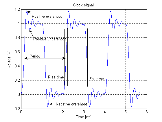
A clock signal is a periodic electrical signal that oscillates between high and low voltage states, typically in the form of a square wave, serving as a fundamental timing reference in digital circuits.[6] It coordinates the operations of sequential logic elements, such as flip-flops and registers, by providing precise timing cues that dictate when state changes occur.[7] This synchronization ensures that data transfers, computations, and control signals propagate reliably across interconnected components, such as in processors and memory systems.[8] The primary purpose of a clock signal is to enable orderly execution in synchronous digital systems, where all elements operate in lockstep to avoid timing conflicts like race conditions that could lead to unpredictable outcomes.[9] By defining discrete time intervals for actions, it facilitates predictable behavior, allowing complex operations to be broken into manageable steps that align across the circuit.[10] In essence, the clock acts as the "heartbeat" of the system, maintaining rhythm and preventing asynchronous chaos in devices ranging from microcontrollers to high-performance computing hardware.[8] The concept of the clock signal originated in the early 1940s amid the development of the first electronic digital computers, where it was essential for managing the switching times of vacuum tubes and synchronizing pulse-based operations.[11] It gained prominence with the ENIAC, completed in 1945, which employed a dedicated cycling unit as its central clock to orchestrate the timing of computations across its 18,000 vacuum tubes, ensuring all units pulsed in unison.[12] In its basic form, the clock waveform features sharp rising edges (transitions from low to high) and falling edges (from high to low), which mark the boundaries of each clock cycle and trigger logic events.[6] The duty cycle, representing the proportion of the cycle spent in the high state, is ideally 50% to provide symmetric timing for both edges, optimizing performance in most digital applications.[9]Key Characteristics
The frequency of a clock signal, measured in hertz (Hz), represents the number of cycles per second and dictates the operational speed of digital circuits, such as enabling modern central processing units (CPUs) to perform billions of instructions per second at frequencies around 1 GHz or higher. The period , which is the duration of one complete cycle, is inversely related to frequency by the equation , where is the frequency; for instance, a 1 GHz clock has a period of 1 nanosecond.[13][14] The amplitude of a clock signal refers to the voltage swing between its low (logic 0) and high (logic 1) states, typically ranging from 0 V to the supply voltage , such as 5 V in traditional transistor-transistor logic (TTL) or 3.3 V in complementary metal-oxide-semiconductor (CMOS) logic families. In TTL, valid low levels are 0–0.8 V and high levels are 2–5 V, while CMOS levels are more rail-to-rail, with low near 0 V and high near , ensuring compatibility across devices. Rise and fall times, defined as the duration for the signal to transition from 20% to 80% (or vice versa) of its amplitude, critically influence edge sharpness; slower transitions (e.g., exceeding 10% of the period) can degrade timing precision in high-speed applications.[15][16] The duty cycle of a clock signal is the ratio of the high-state duration to the total period, expressed as a percentage, with an ideal value of 50% providing balanced timing for both rising- and falling-edge operations in symmetric circuits. Deviations from 50%, such as a 40% duty cycle, introduce imbalances that may violate minimum pulse-width requirements in flip-flops, leading to unreliable state changes or reduced maximum frequency.[13] Clock signals drive sequential elements in either edge-triggered or level-sensitive modes, with most contemporary digital systems favoring edge-triggered behavior for precise synchronization. Edge-triggered circuits, typically implemented with flip-flops, capture input data only at the rising (positive-edge) or falling (negative-edge) transition of the clock, ensuring a single, well-defined sampling point per cycle and minimizing race conditions. In contrast, level-sensitive circuits, such as latches, respond to the sustained clock level (e.g., high or low), allowing continuous transparency during that phase but risking feedback loops if inputs change while enabled.[17][1] Clock signals are highly susceptible to noise, which can distort edges and induce metastability in synchronizing elements like flip-flops. Clean, sharp edges are essential to resolve input setups within the setup and hold time windows; noise-induced jitter or slow transitions increase the probability of metastability, where the output remains in an indeterminate state, potentially propagating errors through the circuit. Techniques like hysteresis in receivers help mitigate noise by providing distinct thresholds for rising and falling transitions.Types in Digital Circuits
Single-Phase Clock
A single-phase clock consists of a solitary periodic waveform that synchronizes operations across digital circuits, typically employing edge-triggered mechanisms where actions are initiated on the rising or falling edge of the signal, though level-sensitive latches may respond to the clock's high or low phase.[18] This structure contrasts with multi-phase systems by using one clock line to drive all components, ensuring uniform timing without additional phase signals.[1] In applications, single-phase clocks are prevalent in basic synchronous designs such as D flip-flops, counters, and finite state machines, particularly in early integrated circuits like the 7400 series TTL logic family. For instance, the 74LS74 dual D flip-flop IC operates with a single clock input to capture data on the rising edge, enabling sequential logic in counters like the 74LS90 decade counter for frequency division tasks.[19] These components form the backbone of simple state machines in legacy systems, where the clock dictates state transitions without phase interleaving.[20] The primary advantages of a single-phase clock include minimal wiring requirements and inherent simplicity, as it eliminates the need for phase coordination or multiple clock lines, thereby reducing design complexity and power overhead in distribution networks.[18] This approach also facilitates time borrowing in latch-based pipelines, allowing critical paths to extend beyond a single cycle for improved performance in high-speed applications.[1] However, limitations arise from its reliance on precise edge timing, particularly the risk of hold time violations when input data changes too soon after the clock edge, potentially causing metastable states or incorrect latching in flip-flops.[21] Such issues demand rigorous verification of short-path delays to ensure data stability, complicating design in high-frequency environments where clock skew exacerbates hold constraints.[18] A representative example is the D flip-flop circuit, where the output Q follows the D input value upon the active clock edge, synchronizing data propagation in sequential logic. In this setup, the single-phase clock ensures that state updates occur predictably, but only if timing margins are met.[20] To illustrate setup and hold times relative to the single clock edge in a D flip-flop, consider the following conceptual timing diagram (positive edge-triggered):CLK: ____|‾‾‾‾|____|‾‾‾‾|____
t_su | t_hold
D: ________| |______
D1 D2
Q: ________| |________ (Q follows D1 after edge)
CLK:   ____|‾‾‾‾|____|‾‾‾‾|____
       t_su    |     t_hold
D:     ________|     |______
              D1         D2
Q:     ________|     |________  (Q follows D1 after edge)