Hubbry Logo
Indium antimonideIndium antimonideMain
Open search
Indium antimonide
Community hub
Indium antimonide
logo
8 pages, 0 posts
0 subscribers
Be the first to start a discussion here.
Indium antimonide
Indium antimonide
from Wikipedia
Indium antimonide
Ball and stick cell model of indium antimonide
Sample of crystalline indium antimonide
Identifiers
3D model (JSmol)
ChemSpider
ECHA InfoCard 100.013.812 Edit this at Wikidata
EC Number
  • 215-192-3
RTECS number
  • NL1105000
UNII
UN number 1549
  • InChI=1S/In.Sb checkY
    Key: WPYVAWXEWQSOGY-UHFFFAOYSA-N checkY
  • [In]#[Sb]
Properties
InSb
Molar mass 236.578 g·mol−1
Appearance Dark grey, metallic crystals
Density 5.7747 g⋅cm−3[1]
Melting point 524 °C (975 °F; 797 K)[1]
Band gap 0.17 eV
Electron mobility 7.7 mC⋅s⋅g−1 (at 27 °C)
Thermal conductivity 180 mW⋅K−1⋅cm−1 (at 27 °C)
4[2]
Structure
Zincblende
T2d-F-43m
a = 0.648 nm
Tetrahedral
Thermochemistry[3]
49.5 J·K−1·mol−1
86.2 J·K−1·mol−1
−30.5 kJ·mol−1
−25.5 kJ·mol−1
Hazards
GHS labelling:
GHS07: Exclamation mark GHS09: Environmental hazard
Warning
H302, H332, H411
P273
Related compounds
Other anions
Indium nitride
Indium phosphide
Indium arsenide
Except where otherwise noted, data are given for materials in their standard state (at 25 °C [77 °F], 100 kPa).
checkY verify (what is checkY☒N ?)

Indium antimonide (InSb) is a crystalline compound made from the elements indium (In) and antimony (Sb). It is a narrow-gap semiconductor material from the III-V group used in infrared detectors, including thermal imaging cameras, FLIR systems, infrared homing missile guidance systems, and in infrared astronomy. Indium antimonide detectors are sensitive to infrared wavelengths between 1 and 5 μm.

Indium antimonide was a very common detector in the old, single-detector mechanically scanned thermal imaging systems. Another application is as a terahertz radiation source as it is a strong photo-Dember emitter.

History

[edit]

The intermetallic compound was first reported by Liu and Peretti in 1951, who gave its homogeneity range, structure type, and lattice constant.[4] Polycrystalline ingots of InSb were prepared by Heinrich Welker in 1952, although they were not very pure by today's semiconductor standards. Welker was interested in systematically studying the semiconducting properties of the III-V compounds. He noted how InSb appeared to have a small direct band gap and a very high electron mobility.[5] InSb crystals have been grown by slow cooling from liquid melt at least since 1954.[6]

In 2018, a research team at Delft University of Technology claimed that indium antimonide nanowires showed potential application in creating Majorana zero mode quasiparticles for use in quantum computing; Microsoft opened a laboratory at the university to further this research, however Delft later retracted the paper.[7][8]

Physical properties

[edit]

InSb has the appearance of dark-grey silvery metal pieces or powder with vitreous lustre. When subjected to temperatures over 500 °C, it melts and decomposes, liberating antimony and antimony oxide vapors.

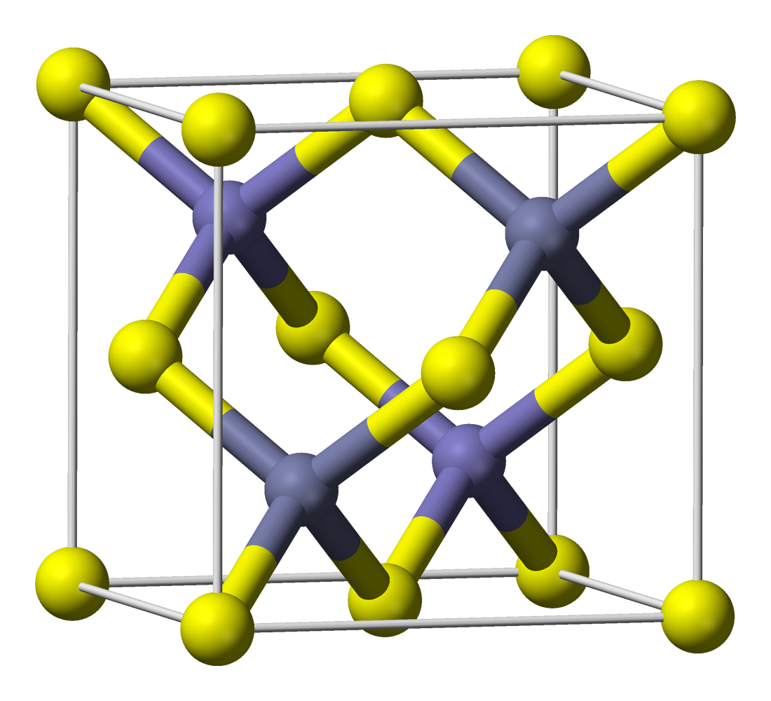
The crystal structure is zincblende with a 0.648 nm lattice constant.[9]

Electronic properties

[edit]
InSb infrared detector manufactured by Mullard in the 1960s.

InSb is a narrow direct band gap semiconductor with an energy band gap of 0.17 eV at 300 K and 0.23 eV at 80 K.[9]

Undoped InSb possesses the largest ambient-temperature electron mobility of 78000 cm2/(V⋅s),[10] electron drift velocity, and ballistic length (up to 0.7 μm at 300 K)[9] of any known semiconductor, except for carbon nanotubes.

Indium antimonide photodiode detectors are photovoltaic, generating electric current when subjected to infrared radiation. InSb's internal quantum efficiency is effectively 100% but is a function of the thickness particularly for near bandedge photons.[11] Like all narrow bandgap materials InSb detectors require periodic recalibrations, increasing the complexity of the imaging system. This added complexity is worthwhile where extreme sensitivity is required, e.g. in long-range military thermal imaging systems. InSb detectors also require cooling, as they have to operate at cryogenic temperatures (typically 80 K). Large arrays (up to 2048×2048 pixels) are available.[12] HgCdTe and PtSi are materials with similar use.

A layer of indium antimonide sandwiched between layers of aluminium indium antimonide can act as a quantum well. In such a heterostructure InSb/AlInSb has recently been shown to exhibit a robust quantum Hall effect.[13] This approach is studied in order to construct very fast transistors.[14] Bipolar transistors operating at frequencies up to 85 GHz were constructed from indium antimonide in the late 1990s; field-effect transistors operating at over 200 GHz have been reported more recently (Intel/QinetiQ).[citation needed] Some models suggest that terahertz frequencies are achievable with this material. Indium antimonide semiconductor devices are also capable of operating with voltages under 0.5 V, reducing their power requirements.[citation needed]

Growth methods

[edit]

InSb can be grown by solidifying a melt from the liquid state (Czochralski process), or epitaxially by liquid phase epitaxy, hot wall epitaxy or molecular beam epitaxy. It can also be grown from organometallic compounds by MOVPE.[citation needed]

Device applications

[edit]

References

[edit]

Cited sources

[edit]
[edit]
Revisions and contributorsEdit on WikipediaRead on Wikipedia
from Grokipedia
Indium antimonide (InSb) is a narrow-bandgap III-V compound semiconductor consisting of indium and antimony in a 1:1 stoichiometric ratio, crystallizing in the zinc blende structure with space group F4ˉ\bar{4}3m and a lattice constant of 6.479 Å at 300 K. Its direct bandgap is 0.17 eV at room temperature, enabling strong absorption in the mid-wave infrared (MWIR) region from 3 to 5 μm, while its density is 5.77 g/cm³ and it features an exceptionally high electron mobility of approximately 78,000 cm²/V·s—the highest among III-V semiconductors—along with a light effective electron mass of 0.014 m₀. These properties position InSb as a key material for optoelectronic applications, particularly in cooled photovoltaic detectors for imaging systems such as (FLIR) cameras and thermal imagers used in military surveillance, medical , and . It also serves as a source due to its strong photo-Dember effect and finds use in high-speed sensors and devices owing to its high carrier mobilities and low effective masses. Advances include room-temperature mid- photodiodes and flexible detectors based on InSb nanowires, expanding its potential in portable and spintronic applications leveraging its large g-factor and strong spin-orbit coupling. As of 2025, further developments involve InSb colloidal quantum dots with defect modulation for improved mid- photodetection and thermally tunable terahertz metasurfaces.

Structure and composition

Crystal structure

Indium antimonide (InSb) crystallizes in the zincblende structure, a face-centered cubic lattice common to III-V compound semiconductors, where and atoms occupy alternating positions in a tetrahedral coordination. The unit cell of this structure contains four In atoms and four Sb atoms, forming a network of corner-sharing tetrahedra that define the overall atomic arrangement. At , the of InSb is 0.6479 nm, making it one of the largest among III-V compounds. This parameter determines the spacing between atomic planes and influences the material's compatibility with other semiconductors in heterostructures. The In-Sb within the lattice is approximately 0.28 nm, which is notably longer than the 0.245 nm Ga-As bond in (GaAs), attributable to the larger atomic radii of and compared to and . The zincblende arrangement corresponds to the F-43m (No. 216), which lacks a center of inversion and thereby enables piezoelectric responses under mechanical stress. This structural feature arises from the polar nature of the III-V bonding and contributes to electromechanical effects observed in InSb devices. The also has implications for the , promoting direct bandgap transitions aligned with the lattice's tetrahedral geometry.

Stoichiometry and defects

Indium antimonide (InSb) possesses an ideal 1:1 of to , which is essential for achieving optimal lattice perfection in its zincblende and minimizing unintended electrical activity. Deviations from this , particularly under In-rich growth conditions, introduce excess that promotes the formation of donor defects, resulting in intrinsic n-type conductivity. For instance, Sb-deficient compositions lead to Sb vacancies that act as shallow donors, elevating concentrations and influencing overall material performance. Native point defects in InSb encompass vacancies, interstitials, and antisite disorders, each altering the local atomic arrangement and electronic structure. Sb vacancies (VSb) serve as donors, facilitating n-type behavior by donating electrons to the conduction band, while In vacancies (VIn) function as triple acceptors, potentially enabling p-type characteristics under Sb-rich conditions. Interstitial defects, such as In interstitials (Ini), are also donor-like and prevalent in non-stoichiometric samples, whereas Sb interstitials (Sbi) tend to act as acceptors. Antisite defects include In on Sb sites (InSb), which behave as donors, and Sb on In sites (SbIn), which are acceptors, often forming in off-stoichiometric environments and contributing to compensation effects. Density functional theory (DFT) calculations reveal that formation energies of these defects vary with and , governing their equilibrium concentrations. These energies underscore why donor defects like VSb dominate in as-grown InSb, often requiring controlled synthesis to suppress them. Impurity incorporation thresholds in InSb allow precise tuning of electrical properties by substituting atoms on lattice sites, with solubility limits dictating effective doping ranges. Common donors like (Te) enable high electron densities without phase segregation, while acceptors such as (Zn) facilitate p-type conversion. Beyond these thresholds, excess impurities precipitate as secondary phases, reducing carrier mobility and introducing additional scattering centers.

Physical properties

Mechanical properties

Indium antimonide (InSb) exhibits mechanical properties characteristic of III-V semiconductors, with relatively low stiffness due to its zincblende crystal structure. The Young's modulus along the direction is approximately 40.9 GPa, while the Poisson's ratio is 0.35; these values are derived from measurements of phonon dispersion relations via elastic constants. In terms of hardness, InSb displays Vickers hardness values in the range of 200-300 HV, depending on the crystallographic face and load conditions, with observed between the indium-terminated and antimony-terminated {111} faces—the former being harder. Like other covalent semiconductors, InSb is brittle under mechanical stress, limiting its and making it prone to rather than deformation at . The material's cleavage occurs preferentially along the {110} planes, which is inherent to the zincblende structure and facilitates clean fracture surfaces for device fabrication. Elastic constants of InSb show dependence, with the longitudinal constant C11 decreasing from about 66.7 GPa at 300 K as increases, reflecting softening of the lattice vibrations; this trend is captured in quasiharmonic approximations from simulations.

Thermal properties

Indium antimonide (InSb) possesses a lattice thermal conductivity of approximately 18 W/m·K at 300 K, dominated by - processes that limit heat transport through the crystal lattice. This value reflects the material's intrinsic dynamics in its blende structure, where becomes prominent at , reducing the of s. The of InSb is around 0.2 J/g·K at , corresponding to a temperature of 160 K, which characterizes the vibrational modes contributing to . The linear coefficient of measures 5.37 × 10^{-6} K^{-1}, indicating moderate dimensional changes under due to anharmonic lattice vibrations. InSb melts congruently at 527 °C, but exposure to temperatures above 500 °C leads to , primarily releasing and vapors as the compound dissociates. This phase instability arises from the volatility of its constituent elements, impacting processing conditions for high-temperature applications.

Electronic properties

Band structure

Indium antimonide (InSb) is a narrow-gap direct bandgap , with the conduction band minimum and valence band maximum both located at the Γ point in the , a consequence of its zincblende crystal symmetry. This direct transition facilitates efficient radiative recombination and underpins its applications in infrared optoelectronics. The bandgap energy EgE_g at (300 ) is 0.17 eV, increasing to 0.23 eV at 80 K due to reduced thermal broadening of the bands. The temperature dependence of the bandgap follows a Varshni empirical relation, accounting for electron-phonon interactions and lattice expansion: Eg(T)=0.246.0×104T2T+500eVE_g(T) = 0.24 - \frac{6.0 \times 10^{-4} T^2}{T + 500} \, \text{eV} This formula, fitted to experimental data, predicts the observed narrowing of the gap with increasing temperature, from approximately 0.24 eV near 0 to 0.17 eV at 300 . The effective es of charge carriers in InSb are notably anisotropic and small near the band edges, reflecting the steep dispersion relations. For electrons in the conduction band, the effective is me=0.014m0m_e^* = 0.014 m_0, where m0m_0 is the free electron , high velocities and quantum effects at modest fields. Heavy-hole effective is mh=0.4m0m_h^* = 0.4 m_0, significantly larger due to the flatter valence band curvature. Strong spin-orbit coupling in InSb leads to a large splitting of the valence band, with ΔSO0.8\Delta_{SO} \approx 0.8 eV between the heavy/light-hole and split-off bands, influencing selection rules for optical transitions. Additionally, the conduction band displays non-parabolicity arising from interactions with higher-lying bands, described by the relation E(1+αE)=2k22meE(1 + \alpha E) = \frac{\hbar^2 k^2}{2 m_e^*}, where α4.1\alpha \approx 4.1 eV1^{-1} quantifies the energy-dependent deviation from parabolic dispersion. This non-parabolicity becomes prominent for energies comparable to the small bandgap, affecting high-field transport.

Carrier mobility and doping

Indium antimonide (InSb) is renowned for its exceptional transport properties, primarily due to the low effective mass of , me0.014m0m_e^* \approx 0.014 m_0, where m0m_0 is the free electron mass. This results in an μe\mu_e of up to 78,000 cm²/V·s at 300 K, the highest among III-V semiconductors, enabling rapid transport with minimal . The high mobility arises predominantly from reduced effective mass and low interactions in the narrow-bandgap material, though ionized impurity can limit it in doped samples. In contrast, hole mobility μh\mu_h in InSb is approximately 850 cm²/V·s at , reflecting the heavier effective mass of holes (mh0.4m0m_h^* \approx 0.4 m_0) and stronger scattering mechanisms. In intrinsic or compensated regions where both electrons and holes contribute significantly, dominates carrier dynamics, coupling electron and hole motion through the internal to maintain charge neutrality. This process is particularly pronounced in InSb due to its high intrinsic carrier density near . Intentional doping modifies the carrier type and concentration in InSb to tailor its electrical properties. N-type doping is achieved using tellurium (Te) or selenium (Se) as shallow donors, with ionization energies of about 0.7 meV, allowing nearly complete ionization even at low temperatures. These dopants introduce electrons into the conduction band, with carrier concentrations controllable up to 101810^{18} cm⁻³ while preserving high mobilities in optimized growth conditions. P-type doping employs zinc (Zn) or beryllium (Be) as acceptors, featuring ionization energies around 10 meV, which results in somewhat deeper levels compared to donors and requires higher temperatures for full activation. Carrier concentrations in doped InSb are routinely measured using the , where the Hall coefficient RH=1/(ne)R_H = 1/(n e) for n-type material— with nn the and ee the —provides direct quantification of nn from the transverse voltage under applied . For p-type samples, the sign of RHR_H reverses, yielding hole density via RH=1/(pe)R_H = 1/(p e), where pp is the hole concentration. This technique is essential for characterizing doping efficacy and mobility in InSb heterostructures and bulk crystals.

Optical properties

Absorption and refraction

Indium antimonide (InSb) exhibits strong optical absorption above its bandgap energy EgE_g, primarily due to interband transitions, with the absorption coefficient α\alpha exceeding 104cm110^4 \, \mathrm{cm}^{-1} in the mid-infrared region with a cutoff of approximately 7 μ\mum at . This high absorption enables efficient interaction over short penetration depths, typically on the order of microns, making InSb suitable for mid-IR photonic devices. The absorption onset is determined by the material's narrow bandgap, approximately 0.17 eV at , beyond which α\alpha rises sharply to values around 105cm110^5 \, \mathrm{cm}^{-1} near the edge. The refractive index nn of InSb in the mid-IR is approximately 3.96 at 5 μ\mum, decreasing slightly at longer wavelengths due to dispersion effects. The wavelength dependence of nn follows the , which provides an empirical fit to experimental data across the infrared spectrum, accounting for contributions from electronic transitions and lattice vibrations. In extrinsic InSb samples with significant free carrier concentrations, absorption at longer wavelengths is dominated by free carrier effects, modeled by the Drude theory where αλ2\alpha \propto \lambda^2. This quadratic wavelength dependence arises from intraband scattering of carriers by phonons and impurities, leading to increased losses in the far-infrared. For highly doped InSb, the reflectivity features a plasma edge around 20 μ\mum, resulting from the plasma frequency of free carriers where the real part of the dielectric function crosses zero. This edge shifts with carrier and manifests as a minimum in reflectivity, influencing the material's interaction with far-IR radiation.

Emission and detection

Indium antimonide (InSb) exhibits radiative recombination primarily through band-to-band transitions, resulting in (PL) emission near its direct bandgap energy. At 300 K, the PL peak occurs at approximately 7 μm, corresponding to the room-temperature bandgap of 0.17 eV. This peak shifts to longer wavelengths with increasing temperature due to the negative temperature coefficient of the bandgap, which decreases by about 4 × 10^{-4} eV/K in this range, enabling tunable mid-infrared emission but also leading to thermal broadening and reduced intensity at higher temperatures. In photodetection applications, InSb's narrow bandgap and strong absorption in the mid-infrared enable high quantum efficiency in IR photodiodes, typically ranging from 50-70% across the 1-5 μm spectral window, attributed to efficient carrier generation and collection facilitated by the material's high exceeding 70,000 cm²/V·s at low temperatures. For cryogenic operation at around 77 K, InSb detectors achieve low (NEP) values on the order of 10^{-12} W/√Hz, limited primarily by generation-recombination noise and , making them suitable for high-sensitivity and . Room-temperature performance in both emission and detection is severely constrained by dominant Auger recombination, a non-radiative process with a coefficient of approximately 5 × 10^{-26} cm⁶/s, which shortens carrier lifetimes to picoseconds and quenches luminescence efficiency while increasing dark current in detectors. This mechanism involves intraband transitions where energy is transferred to a third carrier, prevalent in narrow-gap semiconductors like InSb due to the small bandgap and high intrinsic carrier density near 300 K.

Synthesis and growth

Bulk growth techniques

Indium antimonide (InSb) single crystals are primarily grown from the melt using bulk techniques to produce large, high-purity ingots suitable for substrate applications in detectors and electronics. The involves dipping a into the molten InSb, typically contained in a or within a resistance furnace, and slowly pulling it upward while rotating to form a cylindrical boule. Typical growth parameters include a pulling rate of 0.5–1 mm/min to ensure stable interface morphology and minimize defects, with seed rotation rates of 10–20 rpm to promote convective mixing in the melt and uniform control. This technique has yielded ingots up to 50 mm in , though larger diameters require modified two-stage processes for thermal stability. The Bridgman technique, often employed in vertical or horizontal configurations, translates a along a sealed containing the stoichiometric InSb melt to induce from one end. In the vertical Bridgman variant, ampoules with conical tips (15–20° angle) and diameters of 1.5–2 cm are lowered at rates of 1–3 mm/h through a gradient of 10–60°C/cm, producing twin-free crystals 4–6 cm long. Horizontal Bridgman uses similar rates but with tilted ampoules to facilitate . , a refinement of Bridgman, involves repeated passage of a narrow molten zone to achieve purities exceeding 99.999% by segregating impurities to the ends of the . Growth of InSb is challenged by its low (527°C), which promotes in the melt and at the solid-liquid interface, exacerbated by constitutional arising from low segregation coefficients (k ≈ 0.3) for common impurities like . These effects lead to solute rejection ahead of the interface, increasing local melt concentration and reducing the effective , often resulting in polycrystalline regions or inclusions unless mitigated by optimized gradients and vibration-free setups. The low thermal conductivity of InSb further influences melt stability, requiring precise furnace control to avoid constitutional . High-purity undoped InSb crystals achieved via these methods exhibit carrier concentrations below 10^{14} cm^{-3}, enabling low residual doping and high electron mobilities essential for device performance, with etch-pit densities as low as 10^{2}–10^{3} cm^{-2} indicating minimal dislocations. Yields are typically 70–80% single-crystal material after impurity end-cropping in zone-refined ingots.

Thin-film and nanostructure methods

Thin films of indium antimonide (InSb) are primarily fabricated using molecular beam epitaxy (MBE), a vacuum-based technique that enables atomically precise deposition on lattice-mismatched GaAs substrates despite the 7.8% lattice constant difference. Growth proceeds at substrate temperatures of 400–430 °C under ultrahigh vacuum conditions, with typical rates of 0.5–1 μm/h controlled by the indium flux, often set at approximately 3×10^{14} atoms/cm²·s. This method produces smooth, high-mobility layers, such as 4.8 μm-thick films with electron mobilities exceeding 90,000 cm²/V·s at 77 K, by maintaining an Sb/In flux ratio near 1:1.2 to promote stoichiometric incorporation and minimize antimony desorption. Metalorganic vapor phase epitaxy (MOVPE), also known as organometallic vapor-phase epitaxy, offers scalable deposition of InSb thin films using metalorganic precursors trimethylindium (TMIn) and triethylantimony (TESb) in a carrier gas ambient. Optimal requires a V/III ratio exceeding 10, typically fixed at 11, to compensate for the lower cracking efficiency of TESb compared to indium sources and ensure balanced In:Sb incorporation. Growth temperatures range from 435–485 °C, where the process is thermally activated with an apparent of 25 kcal/mol for TMIn-TESb combinations, yielding single-phase InSb layers on GaAs or InSb substrates without significant . This technique is valued for its compatibility with doping and heterostructure integration, though it demands precise precursor flow control to avoid carbon contamination from incomplete . For nanostructured forms, InSb nanowires are synthesized via the vapor-liquid-solid (VLS) mechanism, where Au nanoparticles serve as catalysts to mediate one-dimensional growth from vapor-phase precursors. Using 60 nm Au colloids on InSb(111) substrates, nanowires with diameters of 80–200 nm and lengths up to several micrometers form at 400 °C over 30–50 minutes in a sealed quartz tube reactor, with the InSb source heated to 540 °C to generate vapor. The liquid Au-In-Sb alloy droplet at the growth tip dictates the nanowire diameter and promotes epitaxial alignment, resulting in defect-reduced, zinc-blende structured wires suitable for studies. Post-2020 advances in colloidal (CQD) synthesis have enabled solution-processable InSb nanoparticles through nonpyrophoric routes, such as mixing chloride (InCl₃) and chloride (SbCl₃) precursors in with additives, followed by injection of a like alane N,N-dimethylethylamine at 260 °C for 15–45 minutes. This yields nearly monodisperse CQDs, where quantum confinement tunes the bandgap from the bulk 0.17 eV to 0.98–1.26 eV, extending absorption into the short-wave (~0.98–1.27 μm). A critical postsynthesis exchange replaces long-chain with short ligands (e.g., or methylammonium iodide) via a two-phase / process, often aided by acetic acid, to enhance colloidal stability, reduce inter-dot spacing, and facilitate solid-state film formation with minimal defects. More recent 2025 developments include a stepwise strategy producing larger monodisperse InSb CQDs (5.8–22.2 nm) with absorption exceeding 3000 nm in the mid-, further broadening applications in . These methods collectively allow InSb nanostructures to be integrated into flexible devices while preserving high carrier mobilities.

History

Discovery and early developments

The intermetallic compound (InSb) was first synthesized in 1952 by T. S. and E. A. Peretti through direct fusion of elemental and , establishing its , homogeneity range, zinc blende crystal structure, and of approximately 6.479 Å. In 1952, Heinrich Welker at Laboratories prepared polycrystalline samples of InSb by melting stoichiometric mixtures, revealing its exceptionally narrow direct bandgap of about 0.17 eV at and high exceeding 50,000 cm²/V·s, which highlighted its promise for applications including in the spectrum. By 1954, single crystals of InSb were successfully grown using zone leveling techniques, a refinement of zone melting that improved purity and enabled detailed electrical characterization, such as measurements confirming n-type conduction and mobilities up to 80,000 cm²/V·s at 77 K. During the mid-1950s, early patents emerged recognizing InSb's potential for detection; for instance, a 1952 filing by Heinrich Welker, assigned to Siemens-Schuckertwerke AG, described devices incorporating InSb for detector applications.

Recent research milestones

In the 1980s, researchers began developing antimonide-based quantum wells, including those incorporating InSb, to enable high-electron-mobility transistors (HEMTs) with enhanced carrier transport properties. These structures leveraged the narrow bandgap and high of InSb to form two-dimensional electron gases suitable for high-speed . A notable milestone occurred in 2018 when scientists at reported quantized conductance in InSb nanowires proximitized by superconductors, interpreted as evidence of Majorana fermions for potential applications. However, the paper was retracted in 2021 following independent analyses that identified irregularities in data processing and selection, though the underlying nanowire fabrication techniques advanced hybrid superconductor-semiconductor systems. Post-2020 research has focused on defect modulation in colloidal InSb quantum dots to improve stability and in photodetection. For instance, a 2025 study demonstrated that advanced passivation strategies, such as ligand engineering to suppress surface traps, significantly enhanced extraction and responsivity in short-wave devices. In the , InSb has been integrated into heterostructures and spintronic devices, with strain engineering enabling precise bandgap tuning to realize topological phases. Strain-induced modifications in monolayer InSb, for example, have been shown to open or close bandgaps, facilitating spin-orbit generation and protected edge states for low-dissipation . These advances build on surface repair techniques for InSb-based two-dimensional electron gases, enhancing their suitability for topological and spin manipulation.

Applications

Infrared detectors

Indium antimonide (InSb) serves as a key material for mid-wavelength infrared (MWIR) photon detectors, leveraging its narrow bandgap to enable sensitive detection in the 1–5 μm spectral range, where its optical properties provide strong absorption in atmospheric windows suitable for thermal imaging. These detectors operate primarily in photovoltaic (PV) mode using p-n junction diodes, which offer low power dissipation, high impedance, and minimal 1/f noise, making them ideal for integration into large-scale focal plane arrays (FPAs). Photoconductive (PC) mode, employing intrinsic material with applied bias for current gain, is less common in arrays due to nonuniformity issues at cryogenic temperatures but finds use in specialized single-element configurations. InSb FPAs have advanced to high-resolution formats, including 2048×2048 pixel arrays with pixel pitches as small as 10–15 μm, enabling detailed imaging over large fields of view. To achieve optimal performance, these detectors require cooling to approximately 77 K, typically via or cryocoolers, which suppresses dark current dominated by generation-recombination (GR) noise mechanisms inherent to the narrow-bandgap . At these temperatures, the spectral response peaks in the 3–5 μm MWIR band, with cutoff wavelengths extending to about 5.5 μm, allowing background-limited performance () under typical operating conditions. A primary figure of merit for InSb detectors is the specific detectivity DD^*, which quantifies signal-to-noise performance normalized to detector area and bandwidth; values reach approximately 1012cmHz/W10^{12} \, \mathrm{cm} \, \sqrt{\mathrm{Hz}} / \mathrm{W}
Add your contribution
Related Hubs
User Avatar
No comments yet.