Community hub
TO-18
View on Wikipedia


In electronics, TO-18 is a designation for a style of transistor metal case. The case is more expensive than the similarly sized plastic TO-92 package. The name is from JEDEC, signifying Transistor Outline Package, Case Style 18.[1]
Construction and orientation
[edit]The typical TO-18 metal can package has a base diameter of 5.6 mm (0.22 in), a cap diameter of 4.70 mm (0.185 in), a cap height of 4.83 mm (0.190 in).[1] The tab is located 45° from pin 1, which is typically the emitter. The lead diameter is nominally 0.45 mm (0.018 in). The leads are arranged in a circle with a diameter of 2.54 mm (0.100 in). The minimum length of the leads is 12.7 mm (0.50 in).
Different manufacturers have different tolerances, and the actual form factor may vary slightly, depending on function.
Uses and variants
[edit]
The 3-lead TO-18 is used for transistors and other devices using no more than three leads. Variants for diodes, photodiodes and LEDs may have only two leads. Light-sensitive or light-emitting devices have a transparent window, lens, or parabolic reflectors in the top of the case rather than a sealed, flat top. For example, diode lasers such as those found in CD players may be packaged in TO-18 cases with a lens.
There are variants with between 2 and 8 leads.
TO-46 / TO-52
[edit]The TO-46[2] and TO-52[3] packages have 3 leads. These packages differ from all other variants in the height of the cap. Instead of 4.83 mm (0.190 in) the cap height is only 3.30 mm (0.130 in) for TO-52 and 1.90 mm (0.075 in) for TO-46.
TO-72
[edit]The package with 4 leads but otherwise with dimensions identical to TO-18, is standardized as TO-72.[4] The fourth wire is typically connected to the metal case as a means of electromagnetic shielding for radio frequency applications.
TO-71
[edit]The TO-71 package has 8 leads (up to three of those may be omitted).[5] The minimum angle between two adjacent leads is 45°.
TO-206
[edit]TO-206 is intended to replace previous definitions of packages with leads arranged in a circle with a diameter of 2.54 mm (0.100 in).[6][7] The different outlines are now defined as variants of TO-206: TO-18 is renamed to TO-206-AA, TO-46 to TO-206-AB, TO-52 to TO-206-AC, TO-72 to TO-206-AF. A new package with 3 leads and a cap height of 1.40 mm (0.055 in) (i.e. smaller than TO-46) is added as TO-206-AD. TO-206-AE does not require a minimum diameter of the leads but is otherwise identical to TO-18. The somewhat unrelated TO-58 package is included as TO-206-AG.
National standards
[edit]| Standards organization | Standard | Designation for | |||
|---|---|---|---|---|---|
| TO-18 | TO-46 | TO-71 | TO-72 | ||
| JEDEC | JEP95[7] | TO-206-AA | TO-206-AB | — | TO-206-AF |
| IEC | IEC 60191[a][8] | C7/B11 | C10/B11 | C7/B12 | |
| DIN | DIN 41876[9][8] | 18A3 | 18A4 | ||
| EIAJ / JEITA | ED-7500A[a][10] | TC-7/TB-8C, TC-7/TB-16C | — | — | TC-7/TB-9C |
| British Standards | BS 3934[a][11][12] | SO-12A/SB3-6A | SO-12C/SB3-6A | SO-12A/SB8-1B | SO-12A/SB4-3 |
| Gosstandart | GOST 18472—88[13] | KT-1-7[b] | KT-35-7[c] | — | KT-1-12[d] |
| Rosstandart | GOST R 57439[14] | ||||
| Kombinat Mikroelektronik Erfurt | TGL 11811[15] | A3/15-3a | — | — | A4/15-4a |
| TGL 26713/07[15] | F1BA3 | — | — | F1CA3 | |
See also
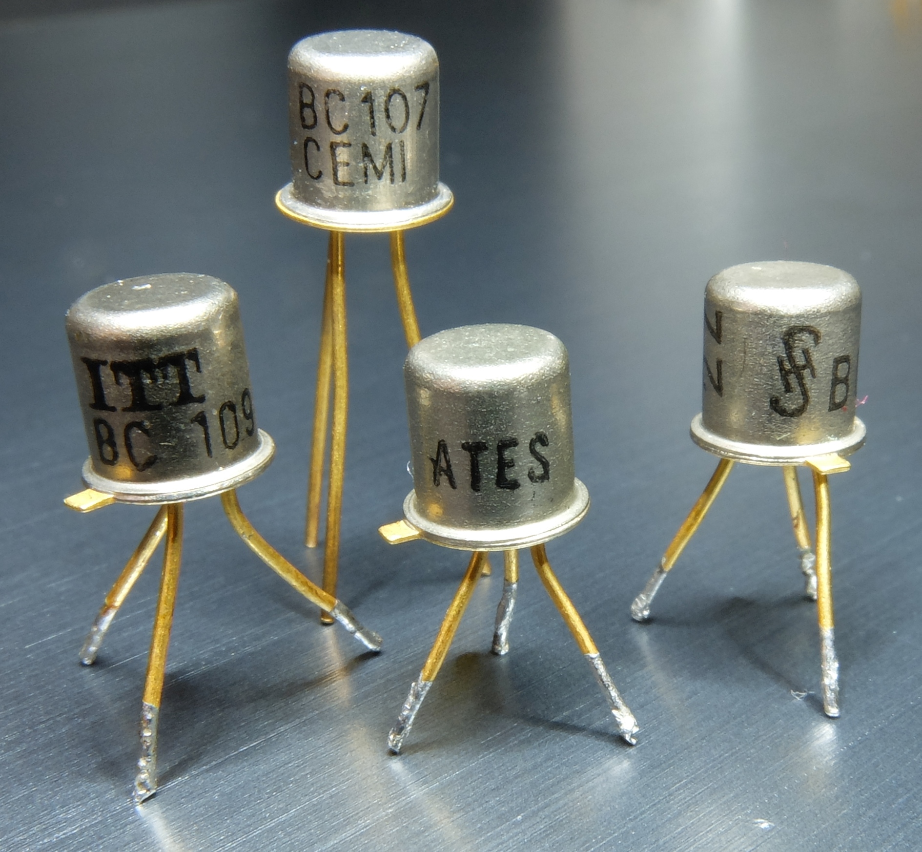
[edit]- Common transistors in a TO-18 package: 2N2222, BC108 family
- Common integrated circuits in a TO-18 package: ZN414
References
[edit]- ^ a b "JEDEC TO-18 package specification" (PDF). JEDEC. Archived from the original (PDF) on June 18, 2017.
- ^ "TO-46" (PDF). JEDEC. Archived from the original (PDF) on 2016-04-04. Retrieved 2021-06-28.
- ^ "TO-52" (PDF). JEDEC. Archived from the original (PDF) on 2016-04-10. Retrieved 2021-06-28.
- ^ "TO-72" (PDF). JEDEC. Archived from the original (PDF) on 2016-04-10. Retrieved 2021-06-28.
- ^ "TO-71" (PDF). JEDEC. Archived from the original (PDF) on 2016-04-10. Retrieved 2021-06-28.
- ^ "Index by Device Type of Registered Transistor Outlines (TO)". JEDEC Publication No. 95 (PDF). JEDEC. October 2010. Retrieved 2021-07-13.
- ^ a b "Header Family 0.100 Pin Circle". JEDEC Publication No. 95 (PDF). JEDEC. November 1982. pp. 182–185. Retrieved 2021-07-13.
- ^ a b "Semiconductors" (PDF). Pro Electron. 1978. p. 215. Retrieved 2021-06-17.
- ^ "Semiconductor Databook" (PDF). Heilbronn: AEG-Telefunken. p. 15. Retrieved 2021-08-20.
- ^ "EIAJ ED-7500A Standards for the Dimensions of Semiconductor Devices" (PDF). JEITA. 1996. Retrieved 2021-06-14.
- ^ "Semiconductor and Photoelectric Devices" (PDF). Mullard. 1968. p. 467. Retrieved 2021-06-14.
- ^ "Mullard Technical Handbook Book 1 Part 1" (PDF). Mullard. September 1974. p. 667. Archived from the original (PDF) on 2021-07-01. Retrieved 2021-07-10.
- ^ "ГОСТ 18472—88 ПРИБОРЫ ПОЛУПРОВОДНИКОВЫЕ - Основные размеры" [GOST 18472—88 Semiconductor devices - basic dimensions] (PDF) (in Russian). Rosstandart. 1988. p. 37-38. Retrieved 2021-06-17.
- ^ "ПРИБОРЫ ПОЛУПРОВОДНИКОВЫЕ - Основные размеры" [Semiconductor devices - basic dimensions] (PDF) (in Russian). Rosstandart. 2017. p. 45. Retrieved 2021-06-17.
- ^ a b "TGL 26713/07: Gehäuse für Halbleiterbauelemente - Bauform F" (PDF) (in German). Leipzig: Verlag für Standardisierung. June 1988. Retrieved 2021-06-15.
External links
[edit]- TO-18 Package, EESemi.com
TO-18
View on GrokipediaOverview and Specifications
Description and Purpose
The TO-18 is a standardized metal can package designated by the Joint Electron Device Engineering Council (JEDEC) as Transistor Outline (TO) Package, Case Style 18, also designated as TO-206-AA in current JEDEC nomenclature, primarily designed for 3-lead transistors, diodes, and similar semiconductor components with low lead counts up to 3 leads, including variants for 1-3 lead configurations.[5] This encapsulation style houses the die within a cylindrical metal enclosure, offering a robust alternative to non-metallic packaging for electronic devices.[4] The primary purpose of the TO-18 is to deliver hermetic sealing, which prevents the ingress of moisture, contaminants, gases, and liquids into the package cavity, thereby safeguarding the internal semiconductor from environmental degradation and ensuring long-term operational reliability.[5] In contrast to more economical plastic alternatives like the TO-92, the TO-18 provides enhanced durability and resistance to harsh conditions, albeit at a higher manufacturing cost, making it preferable for applications requiring sustained performance in challenging environments.[1] Among its general advantages, the TO-18 excels in hermeticity for high-reliability sectors such as aerospace, medical, and military electronics, while its metal construction facilitates superior thermal dissipation compared to plastic packages, aiding in the management of heat from small-signal devices.[6]Physical Dimensions and Materials
The TO-18 package features a cylindrical metal can with a base diameter of 5.6 mm and a cap diameter of 4.70 mm, while the cap height measures 4.83 mm.[7] The leads have a diameter of 0.45 mm and are arranged in a circle with a 2.54 mm diameter, with a minimum lead length of 12.7 mm to facilitate mounting.[7] These dimensions ensure compatibility with standard through-hole assembly processes while providing a compact footprint for small-signal devices.[8] The package typically employs Kovar (ASTM F15 alloy, an iron-nickel-cobalt composition) or Alloy 52 (ASTM F30) for the header and can to achieve hermetic sealing via glass-to-metal bonds.[1] Leads are often gold-plated for enhanced corrosion resistance and solderability, though lead-free options may use matte tin plating.[2] These materials contribute to the package's durability in harsh environments, including resistance to moisture and mechanical stress.[1] The approximate weight of the TO-18 package is approximately 0.3 grams, depending on specific plating and alloy variations, making it lightweight for portable applications.[2] Its thermal properties support low-power dissipation up to 500 mW at an ambient temperature of 25°C, suitable for devices like small-signal transistors without requiring extensive heat sinking.[9] Visually, the TO-18 consists of a flat-based cylindrical metal enclosure, often with an optional orientation tab positioned at a 45° angle from pin 1 to aid in automated handling and assembly.[7] This design provides hermetic protection for internal components, including options for transparent windows in light-sensitive applications.[1]Design and Construction
Assembly and Components
The TO-18 package assembly begins with the header, which serves as the base and incorporates a lead frame for electrical connections, typically constructed from Kovar (ASTM F15 alloy) or Alloy 42 (ASTM F30) to ensure thermal expansion compatibility with the semiconductor die.[1] The semiconductor die is then attached to the header's die pad using epoxy adhesive or solder, such as eutectic bonding, to provide mechanical stability and electrical contact; this step is critical for heat dissipation in high-reliability applications.[10] Following die attachment, gold wires—typically 0.001-inch diameter—are bonded from the die pads to the lead frame pins via thermosonic or thermocompression wire bonding, establishing low-resistance interconnections while maintaining hermetic integrity.[10] The internal structure features the semiconductor die mounted directly on the header, which can be configured as an isolated mount for flexibility in circuit design or a common-base setup where the header connects to one of the leads (often the collector in transistor applications), optimizing for specific device topologies like bipolar junctions.[8] For optoelectronic variants, such as photodiodes or LEDs, the header includes provisions for transparent windows made of sapphire or borosilicate glass, allowing optical access while preserving the hermetic environment.[11] No encapsulation is typically required beyond the hermetic seal, as the metal can design inherently protects against environmental contaminants. The assembly process proceeds with die placement and bonding in a controlled cleanroom environment to minimize particulates, followed by optional encapsulation for non-hermetic interim protection if needed, and culminates in cap attachment.[10] The metal cap, matching the package body diameter of 5.31 to 5.84 mm (0.209 to 0.230 inches), is welded to the header using resistance (high-current) or laser methods under vacuum conditions to evacuate air and moisture, forming a robust hermetic seal with a leak rate of less than 10^{-8} atm-cc/sec.[8] Hermeticity is verified post-assembly through helium leak detection, where packages are pressurized with helium and monitored for fine leaks in accordance with MIL-STD-883, Test Method 1014, ensuring long-term reliability in harsh environments.[12] Quality control in TO-18 assembly adheres to military standards for high-reliability components, including MIL-PRF-19500 for discrete semiconductors, with lead frames and headers plated to specified thicknesses—such as 1-2 μm nickel underplate—for corrosion resistance and solderability. These plating layers, often topped with gold for wire bondability, undergo adhesion and thickness verification to prevent failures in thermal cycling or vibration, supporting applications in aerospace and defense where failure rates must remain below 1% over extended lifespans.[10]Pin Configuration and Orientation
The TO-18 package employs a standard three-lead configuration for bipolar junction transistors, with pin 1 assigned to the emitter, pin 2 to the base, and pin 3 to the collector, arranged in clockwise EBC order when viewed from the bottom (leads facing the viewer) with the flat tab oriented at the top.[2] This pinout convention ensures consistent electrical connectivity and is widely adopted in devices such as the 2N2222 NPN transistor.[13] Orientation is facilitated by a flat tab or dimple on the metal can, positioned at a 45-degree angle clockwise from the emitter lead (pin 1), allowing users to align the package correctly during installation.[13] Some variants include painted markings or color dots on the can to distinguish NPN from PNP types, though identification often relies on the part number etched or printed on the top surface.[14] The leads are spaced 120 degrees apart along a 2.54 mm (0.100 inch) diameter circle at the base of the package, providing mechanical stability and compatibility with standard printed circuit board (PCB) hole patterns.[2] For PCB mounting, leads should be bent at a minimum distance of 1.5 mm from the package body to prevent stress on the internal seals, typically forming a 90-degree angle or custom shape to fit through-hole pads while maintaining lead integrity.[14] While the standard TO-18 is limited to three leads in this radial arrangement, multi-lead variants of similar metal-can packages can accommodate up to eight leads for more complex devices, though these fall outside the core TO-18 outline.[2]History and Development
Origins and Invention
The TO-18 package emerged in the late 1950s as part of the broader Transistor Outline (TO) series standardized by the Joint Electron Device Engineering Council (JEDEC), which was formed in 1958 to establish uniform specifications for solid-state devices following the rapid growth of the semiconductor industry after World War II.[15] This standardization addressed the need for consistent, interchangeable packaging to support the scaling production of transistors, building on earlier proprietary designs to ensure compatibility across manufacturers.[16] The primary drivers for the TO-18's development were the demand for robust, hermetic encapsulation to protect sensitive transistor junctions from moisture, mechanical stress, and thermal extremes, particularly in high-reliability sectors like telecommunications and military electronics. Bell Laboratories, where the transistor was invented in 1947, played a pivotal role through its early adoption of metal-can enclosures—such as the "Type A" cartridge-style packages for point-contact transistors—which influenced the TO series' emphasis on metallic construction for durability and heat dissipation.[17][18] These designs evolved from the post-war push to replace vacuum tubes with more compact, reliable alternatives amid the semiconductor boom.[19] Major semiconductor firms, including Texas Instruments, Fairchild Semiconductor (founded in 1957), and RCA, were among the first to adopt the TO-18 for production, initially packaging germanium transistors before shifting to silicon versions in the early 1960s to capitalize on improved performance and lower costs.[20] For instance, Motorola introduced the influential 2N2222 silicon NPN transistor in a TO-18 case in 1962, marking a key step in the transition from germanium to silicon dominance.[21] This package's three-lead configuration and compact form factor facilitated its integration into diverse applications, accelerating the transistor's role in electronics. By the mid-1960s, the TO-18 had proliferated widely in consumer products, powering early portable radios and nascent computer systems, as its standardized outline enabled mass production and reduced costs compared to custom enclosures.[20] JEDEC's ongoing refinements to the TO outlines, including the TO-18, solidified its status as a foundational package for bipolar junction transistors, supporting the explosive growth of the industry during the decade.[22]Standardization Efforts
The Joint Electron Device Engineering Council (JEDEC) played a central role in standardizing the TO-18 package, defining its outline in Publication 95 (JEP95) through the JC-11 Committee on Mechanical Standardization since the late 1950s.[15][22] This effort followed JEDEC's formation in 1958 to establish uniform standards for solid-state devices, ensuring mechanical interchangeability across manufacturers.[15] The TO-18 outline, originally designated as such, was later updated within the TO-206 series (specifically TO-206AA) in JEP95 to maintain legacy compatibility while accommodating evolving manufacturing practices.[23] International equivalents to the TO-18 package emerged through parallel standardization by bodies such as the International Electrotechnical Commission (IEC) under IEC 60191 for mechanical outlines of semiconductor devices, the German Institute for Standardization (DIN), the Electronic Industries Association of Japan (EIAJ), British Standards (BS), and the Soviet GOST system. Harmonization between JEDEC and these international standards intensified during the 1970s and 1980s, facilitating global adoption and reducing discrepancies in dimensions and pin configurations for transistor packages.[24][25] Key documents supporting TO-18 standardization include JEP95, which details outline drawings, dimensions, and tolerances (such as ±0.1 mm on key diameters like the body and lead circle) to ensure precise fabrication.[26] Complementary standards like MIL-STD-750 establish test methods for semiconductor devices in TO-18 packages, covering environmental, electrical, and mechanical reliability assessments. The standard has evolved with revisions in the 2000s to address lead-free compliance, incorporating guidelines from JESD201 for tin-based finishes and RoHS alignment without altering core dimensions.[27] JEDEC continues ongoing maintenance via the JC-11 committee, particularly for high-reliability applications in aerospace and military sectors, to adapt to material advancements while preserving backward compatibility.[22]Applications and Uses
Traditional Devices
The TO-18 package was widely adopted in the 1960s and 1970s for housing classic bipolar junction transistors (BJTs) in low-power consumer electronics. Among the most common were NPN small-signal transistors like the 2N2222A, which featured a collector-emitter voltage rating of 40 V, a continuous collector current of 800 mA, and a power dissipation of up to 500 mW at 25°C, making it suitable for amplification and switching in audio and RF circuits.[28] Its PNP complement, the 2N2907, offered similar performance characteristics with a collector-emitter voltage of 60 V and power dissipation of 400 mW, enabling complementary pair configurations in push-pull amplifiers. European equivalents such as the BC107 and BC108 series, also NPN types, were prevalent in similar roles, with the BC107 rated for 45 V collector-emitter voltage and 200 mA collector current at 600 mW dissipation, often used in general-purpose amplification within early integrated circuits and discrete designs.[29] These transistors benefited from the TO-18's hermetic metal can, which provided robust environmental protection for the die, typically a planar epitaxial silicon structure bonded via gold wires to the header and pins in a standard configuration of collector (pin 1), base (pin 2), and emitter (pin 3). A cross-section of the 2N2222 reveals the small die (approximately 0.5 mm × 0.5 mm) centrally mounted on the copper-alloy header for heat sinking, with fine bond wires (about 25 μm diameter) extending to the Kovar leads, ensuring reliable high-frequency operation up to transition frequencies of 300 MHz.[30] This construction supported applications in 1960s transistor radios and 1970s-1980s television tuners, where the package's thermal and mechanical stability maintained performance in compact, battery-powered devices.[31] Beyond transistors, the TO-18 housed early small-signal diodes and photodiodes during the same era. Fast-switching diodes were occasionally packaged in TO-18 for enhanced hermetic sealing in high-reliability needs, though glass DO-35 types dominated for general use; these supported signal rectification and clipping in RF front-ends of radios and TVs. Early silicon PIN photodiodes, like precursors to the BPW24R, utilized the TO-18's light-accessible window or clear lid for optical detection in 1960s instrumentation and 1980s consumer remote controls, offering low dark current and responsivity up to 1000 nm. In legacy contexts, TO-18 devices powered military gear, including VHF amplifiers in communication systems, due to the package's durability in harsh environments.[1] Early integrated circuit prototypes, such as the ZN414 AM radio receiver chip, were encapsulated in TO-18 for prototyping in the 1970s, leveraging its three-pin compatibility. By the 1980s, consumer adoption waned as cost-effective plastic alternatives like TO-92 emerged, phasing out TO-18 in non-critical applications while preserving its role in high-reliability sectors.[32]Modern and Specialized Applications
The TO-18 package finds ongoing application as of 2025 in high-reliability sectors including aerospace, military, and medical instruments, where its hermetic metal construction ensures protection against moisture, contaminants, and extreme environmental stresses. In aerospace and military contexts, it is used for sensors and RF modules, such as small-signal transistors in RF circuits for radar and communication systems, meeting MIL-STD-883 for radiation hardness and MIL-PRF-19500 for performance in vacuum and temperature extremes.[33][1] In medical instruments, TO-18-encased components support applications like ECG amplifiers and non-invasive LED sensors for patient monitoring.[33][34] In sensor technologies, the TO-18 package is particularly valued for optoelectronic devices, including phototransistors and LEDs equipped with lenses or windows to facilitate optical signal transmission and detection. These are deployed in communication devices for fiber optic links, such as intra-system conversions in industrial Ethernet equipment, and in photodetectors for precise light sensing in harsh conditions.[35][36] Representative examples include the OSRAM BP 103 silicon phototransistor for general optical detection and TT Electronics' OP598 series for triangulation and long-distance sensing in encoders.[37][38] Production of TO-18 packages persists as of 2025 for legacy system replacements and new designs in demanding environments, with lead-free variants introduced to comply with the 2006 RoHS Directive restricting hazardous substances like lead in electronics.[39] Manufacturers continue to offer RoHS-compliant options, such as infrared LEDs in TO-18 for high-reliability optoelectronics.[39] Today, the TO-18's key advantage lies in its superior hermetic sealing over plastic alternatives, providing airtight protection essential for vacuum exposure in satellite electronics and resistance to thermal cycling in automotive sensors.[33][34] This makes it ideal for space-grade RF modules in satellites and high-temperature pressure sensors in under-hood automotive applications.[33][1]Variants and Related Packages
TO-46 and TO-52
The TO-46 and TO-52 represent shorter-height variants of the TO-18 package, optimized for space-constrained environments while retaining core design principles like hermetic sealing and lead configuration for pin compatibility.[4][6] The TO-46 is a 3-lead package with a cap height of 1.90 mm, enabling its use in ultra-miniature transistors and diodes within highly compact circuits where minimal vertical profile is essential.[40] This reduced height facilitates greater component density on printed circuit boards (PCBs) compared to the standard TO-18, with a smaller base diameter of 4.52 to 4.95 mm (0.178 to 0.195 in) and material properties such as Kovar or steel bases with glass-to-metal seals.[6][41][42] Similarly, the TO-52 employs a 3-lead configuration with a cap height of 3.30 mm, providing an intermediate profile that balances compactness with sufficient internal space for performance-oriented devices.[43] Like the TO-18 (but unlike the TO-46), it shares a base diameter of approximately 5.6 mm and materials but incorporates adjusted sealing techniques to maintain hermetic integrity under reduced height constraints, supporting applications requiring moderate miniaturization without sacrificing thermal or electrical reliability. Note that the TO-52 is a legacy package, declared inactive by JEDEC in 1996, though still available for some devices.[6][23] These variants find applications in low-profile electronic devices where their slim design aids in minimizing overall thickness.[44][45] Representative examples include low-profile 2N series transistors, like the 2N3509 in TO-46 for switching in compact audio circuits and the 2N3009 in TO-52 for amplification in battery-powered portables.[44][45]TO-72 and TO-71
The TO-72 package is a four-lead variant of the metal can transistor outline (redesignated TO-206-AF by JEDEC), designed primarily for high-frequency applications where an additional lead provides dedicated case grounding to minimize electromagnetic interference.[4][23] This configuration maintains the compact cylindrical form factor of the standard TO-18, with a base diameter of approximately 5.59 mm and a lead circle diameter of 0.100 inches, allowing for axial leads suitable for through-hole mounting.[4] The fourth lead connects to the metal case, which acts as an RF shield, enhancing performance in environments prone to noise, such as radio frequency circuits.[46] In contrast, the TO-71 package accommodates up to eight leads in a radial pattern, enabling its use in more complex devices like dual discrete transistors or early integrated circuits requiring multiple connections.[47] It features an enhanced header to support additional wire bonds for intricate die structures, while retaining the same outer diameter as the TO-72 at around 5.6 mm, though its overall height may increase slightly to 6.5-7.5 mm to accommodate taller internal assemblies.[47] The package weighs approximately 0.35 grams and uses a hermetic metal can seal for reliability in demanding conditions.[47] Construction differences in these variants focus on lead expansion for functionality: the TO-72's extra ground lead integrates with the case to reduce parasitic capacitance and improve isolation in RF paths, while the TO-71's multi-lead array supports balanced signaling in multi-element devices, often with optional unpopulated pins for flexibility.[48] Both share gold-plated or tinned leads with a 0.015-0.020 inch diameter, ensuring compatibility with standard soldering processes, and conform to JEDEC outlines for interchangeability.[26] These packages find unique applications in specialized electronics, with the TO-72 commonly employed in RF amplifiers and oscillators, as seen in silicon NPN transistors like the BFW30 for telecom signal processing up to 1.6 GHz.[49] The TO-71 supports early operational amplifiers and matched dual JFETs in low-noise audio and instrumentation circuits, such as the 2N3957 for high-impedance telecom interfaces.[50] Their hermetic design ensures longevity in legacy telecommunications equipment and military-grade RF modules.[51]TO-206 and Legacy Designations
The TO-206 series represents a modern superset of earlier transistor outline designations, established by JEDEC to consolidate and update specifications for metal can packages with a 0.100-inch pin circle diameter. Under this framework, the traditional TO-18 package has been redesignated as TO-206-AA, maintaining its three-lead configuration while incorporating refined dimensional outlines for improved manufacturing consistency. Similarly, variants such as TO-206-AB (formerly TO-46) and TO-206-AC (formerly TO-52, now inactive) accommodate configurations with 3 or 4 leads, allowing for expanded pin arrangements in compact hermetic enclosures. The TO-72 is redesignated as TO-206-AF. This redesignation, formalized in JEDEC Publication 95, ensures that the TO-206 family serves as a unified reference for legacy and contemporary designs without altering core functionality.[23] The TO-206 series addresses legacy designations from the 1950s and 1960s, such as the JAN-TX military specifications for transistors, by providing cross-references that preserve backward compatibility in engineering drawings and procurement documents. For instance, devices qualified under JAN-TX standards, which specified ruggedized metal cans for high-reliability applications, now map directly to TO-206-AA outlines, facilitating seamless transitions in military and aerospace contexts. This compatibility extends to older cataloging systems, where TO-18 equivalents are explicitly noted in modern datasheets to avoid redesign requirements in established systems.[52][53] Key updates in the TO-206 specifications include tighter dimensional tolerances for pin spacing and case dimensions, enhancing solderability and thermal performance compared to original TO-18 outlines, as detailed in JEDEC's registered outlines. Modern implementations also support lead-free plating options to comply with environmental regulations like RoHS, while retaining hermetic sealing for reliability in harsh environments. The primary document governing these outlines is JEDEC Publication 95, which includes detailed drawings for TO-206-AA and related variants, issued with revisions to reflect manufacturing advancements. A practical example of this transition is the 2N2222 transistor, originally specified in TO-18 packaging during the 1960s, now cross-referenced universally as TO-206-AA in current production to maintain interchangeability.[23][54]Standards and Comparisons
JEDEC and International Standards
The TO-18 package, designated as TO-206-AA in current nomenclature, is defined in JEDEC Publication No. 95, which provides detailed outline drawings, dimensions, and tolerances for transistor outlines, including axial lead configurations with a 0.100-inch (2.54 mm) pin circle diameter. Although the TO-18 outline is archived in JEDEC Publication 95, it continues to be used as the standard reference for compatible devices. The body diameter is 0.209 to 0.230 inches (5.31 to 5.84 mm), with tolerances specified to ensure interchangeability in manufacturing and assembly, such as ±0.005 inches (±0.13 mm) on the pin circle diameter. The broader TO-206 family encompasses variants of the TO-18, such as those with modified lead counts or materials, standardized under the same publication to maintain compatibility across semiconductor devices.[55] Internationally, the TO-18 outline aligns with IEC 60191-2, which specifies dimensions for discrete semiconductor device packages, including metal can styles like the TO-18 for ensuring global mechanical standardization. In Europe, Pro Electron coding indirectly references TO-18-compatible packages through transistor designations (e.g., BC107 series), facilitating cross-manufacturer consistency without altering the core package geometry. Russian equivalents are covered under GOST standards, such as GOST R IEC 60191-2 adaptations, which mirror IEC outlines for hermetic metal cans in domestic semiconductor production. Hermeticity testing for TO-18 packages follows MIL-STD-883 Method 1014, requiring a fine leak rate of less than 5 × 10^{-8} atm-cc/sec (measured via helium fine leak or equivalent standard leak rate conversion) to verify seal integrity for microelectronic cavities typically under 0.02 cc.[56] Thermal cycling qualification, per MIL-STD-883 Method 1010, subjects packages to -65°C to +150°C cycles (up to 1000 iterations) to assess reliability under environmental stress, while broader military and space qualifications include vibration, shock, and radiation exposure per the same standard.[56] Revisions in the 2000s addressed lead-free (Pb-free) compliance, with JEDEC updating Publication 95 and introducing JESD201 (2006) to mitigate tin whisker risks in Pb-free finishes, aligning with RoHS Directive 2002/95/EC thresholds (e.g., <1000 ppm Pb).[27] As of 2025, specifications are accessible digitally via the JEDEC website, incorporating ongoing Pb-free material tolerances and RoHS exemptions for high-reliability applications.[57]Comparisons with Other Packages
The TO-18 package provides enhanced durability and hermetic sealing compared to the plastic TO-92, protecting components from moisture and contaminants in high-reliability environments such as aerospace and military applications. In contrast, the TO-92 offers lower cost and easier automation in assembly due to its flexible lead forming and compatibility with high-volume plastic molding processes, though it lacks hermeticity and is more susceptible to environmental degradation. For equivalent devices like the 2N2222 transistor, TO-18 variants typically cost 10-30 times more per unit in low volumes ($1.50-$2.70) than TO-92 versions ($0.05-$0.20), reflecting the added manufacturing complexity of metal fabrication (as of 2024).[1][58][59][60] Relative to the larger TO-5 and TO-39 (also known as TO-205AD) metal can packages, the TO-18 is more compact with a body diameter of approximately 5 mm and base of 5.6 mm, suited for lower-power applications under 1 W dissipation, whereas the TO-39 features a 9 mm base diameter and greater height (up to 12.7 mm in high-profile variants) for improved heat sinking in devices handling 1-5 W. This size trade-off makes the TO-18 preferable for space-constrained designs, but the TO-39's taller profile and larger surface area enable better thermal performance in moderate-power scenarios like RF amplifiers.[2][61][62] As a through-hole metal package, the TO-18 contrasts with the surface-mount plastic SOT-23, which serves as a compact alternative for low-power signal processing with dimensions of 2.9 mm × 1.3 mm × 1 mm, enabling automated pick-and-place assembly but offering inferior mechanical robustness and no hermetic seal. The TO-18's metal construction supports higher reliability ratings, such as MIL-STD compliance for vibration and temperature extremes, at the expense of a bulkier footprint unsuitable for modern dense PCB layouts.[63][1] Key trade-offs across packages include power handling, where the TO-18 supports 0.5-1.2 W dissipation for devices like the 2N2222, outperforming the TO-92's 0.5-0.625 W but falling short of the TO-220's 2 W capacity for higher-current applications. Cost remains a significant factor, with TO-18 at approximately $0.50-$1.00 in moderate volumes versus $0.05 for plastic alternatives like TO-92 or SOT-23, driven by material and sealing processes. In reliability contexts, the TO-18's hermetic design yields superior MTBF in harsh conditions, as evidenced by its use in legacy high-rel systems over non-hermetic plastics.[9][59][60][62]| Package | Material | Typical Power Dissipation | Footprint (mm) | Cost (bulk, per unit) | Key Advantage | Key Disadvantage |
|---|---|---|---|---|---|---|
| TO-18 | Metal (hermetic) | 0.5-1.2 W | Dia: 5 mm | $0.50-$1.00 | Durability, hermetic seal | Higher cost, through-hole |
| TO-92 | Plastic | 0.5-0.625 W | 5 × 5 × 5 | $0.05 | Low cost, easy assembly | Non-hermetic, lower rel. |
| TO-39 | Metal (hermetic) | 1-5 W | Base: 9 mm | $0.75-$1.50 | Better heat sinking | Larger size |
| SOT-23 | Plastic | 0.2-0.5 W | 2.9 × 1.3 × 1 | $0.03-$0.10 | Compact, SMT | Low power, non-hermetic |
| TO-220 | Plastic | 2 W | 10 × 4.5 × 15 | $0.10-$0.20 | High power | Bulky, non-hermetic |