

Community hub
Recent from talks
Contribute something
Nothing was collected or created yet.
Peripheral Component Interconnect
View on Wikipedia
| PCI Local Bus | |
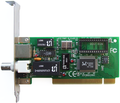
 Three 5-volt 32-bit PCI expansion slots on a motherboard (PC bracket on left side) | |
| Year created | June 22, 1992[1] |
|---|---|
| Created by | Intel |
| Supersedes | ISA, EISA, MCA, VLB |
| Superseded by | AGP for graphics (1997), PCI Express (2004) |
| Width in bits | 32 or 64 |
| Speed | Half-duplex:[2]
133 MB/s (32-bit at 33 MHz – the standard configuration) 266 MB/s (32-bit at 66 MHz) 266 MB/s (64-bit at 33 MHz) 533 MB/s (64-bit at 66 MHz) |
| Style | Parallel |
| Hotplugging interface | Optional |
| Website | www |
Peripheral Component Interconnect (PCI)[3] is a local computer bus for attaching hardware devices in a computer and is part of the PCI Local Bus standard. The PCI bus supports the functions found on a processor bus but in a standardized format that is independent of any given processor's native bus. Devices connected to the PCI bus appear to a bus master to be connected directly to its own bus and are assigned addresses in the processor's address space.[4] It is a parallel bus, synchronous to a single bus clock. Attached devices can take either the form of an integrated circuit fitted onto the motherboard (called a planar device in the PCI specification) or an expansion card that fits into a slot. The PCI Local Bus was first implemented in IBM PC compatibles, where it displaced the combination of several slow Industry Standard Architecture (ISA) slots and one fast VESA Local Bus (VLB) slot as the bus configuration. It has subsequently been adopted for other computer types. Typical PCI cards used in PCs include: network cards, sound cards, modems, extra ports such as Universal Serial Bus (USB) or serial, TV tuner cards and hard disk drive host adapters. PCI video cards replaced ISA and VLB cards until rising bandwidth needs outgrew the abilities of PCI. The preferred interface for video cards then became Accelerated Graphics Port (AGP), a superset of PCI, before giving way to PCI Express.[5]
The first version of PCI found in retail desktop computers was a 32-bit bus using a 33 MHz bus clock and 5 V signaling, although the PCI 1.0 standard provided for a 64-bit variant as well.[6] These have one locating notch in the card. Version 2.0 of the PCI standard introduced 3.3 V slots, physically distinguished by a flipped physical connector to prevent accidental insertion of 5 V cards. Universal cards, which can operate on either voltage, have two notches. Version 2.1 of the PCI standard introduced optional 66 MHz operation. A server-oriented variant of PCI, PCI Extended (PCI-X) operated at frequencies up to 133 MHz for PCI-X 1.0 and up to 533 MHz for PCI-X 2.0. An internal connector for laptop cards, called Mini PCI, was introduced in version 2.2 of the PCI specification. The PCI bus was also adopted for an external laptop connector standard – the CardBus.[7] The first PCI specification was developed by Intel, but subsequent development of the standard became the responsibility of the PCI Special Interest Group (PCI-SIG).[8]
PCI and PCI-X sometimes are referred to as either Parallel PCI or Conventional PCI[9] to distinguish them technologically from their more recent successor PCI Express, which adopted a serial, lane-based architecture.[10][11] PCI's heyday in the desktop computer market was approximately 1995 to 2005.[10] PCI and PCI-X have become obsolete for most purposes and has largely disappeared from many other modern motherboards since 2013; however they are still common on some modern desktops as of 2020[update] for the purposes of backward compatibility and the relative low cost to produce. Another common modern application of parallel PCI is in industrial PCs, where many specialized expansion cards, used here, never transitioned to PCI Express, just as with some ISA cards. Many kinds of devices formerly available on PCI expansion cards are now commonly integrated onto motherboards or available in USB and PCI Express versions.
History
[edit]

Work on PCI began at the Intel Architecture Labs (IAL, also Architecture Development Lab) c. 1990. A team of primarily IAL engineers defined the architecture and developed a proof of concept chipset and platform (Saturn) partnering with teams in the company's desktop PC systems and core logic product organizations.
PCI was immediately put to use in servers, replacing Micro Channel architecture (MCA) and Extended Industry Standard Architecture (EISA) as the server expansion bus of choice. In mainstream PCs, PCI was slower to replace VLB, and did not gain significant market penetration until late 1994 in second-generation Pentium PCs. By 1996, VLB was all but extinct, and manufacturers had adopted PCI even for Intel 80486 (486) computers.[12] EISA continued to be used alongside PCI through 2000. Apple Computer adopted PCI for professional Power Macintosh computers (replacing NuBus) in mid-1995, and the consumer Performa product line (replacing LC Processor Direct Slot (PDS)) in mid-1996.
Outside the server market, the 64-bit version of plain PCI remained rare in practice though,[13] although it was used for example by all (post-iMac) G3 and G4 Power Macintosh computers.[14]
Later revisions of PCI added new features and performance improvements, including a 66 MHz 3.3 V standard and 133 MHz PCI-X, and the adaptation of PCI signaling to other form factors. Both PCI-X 1.0b and PCI-X 2.0 are backward compatible with some PCI standards. These revisions were used on server hardware but consumer PC hardware remained nearly all 32-bit, 33 MHz and 5 volt.
The PCI-SIG introduced the serial PCI Express in c. 2004. Since then, motherboard manufacturers gradually included fewer or zero PCI slots in favor of the new standard. Bridge adapters allow the use of legacy PCI cards with PCI Express motherboards.
| Spec | Year | Change summary[16] |
|---|---|---|
| PCI 1.0 | 1992 | Original issue |
| PCI 2.0 | 1993 | Incorporated connector and add-in card specification |
| PCI 2.1 | 1995 | Incorporated clarifications and added 66 MHz chapter |
| PCI 2.2 | 1998 | Incorporated ECNs, and improved readability |
| PCI 2.3 | 2002 | Incorporated ECNs, errata, and deleted 5 volt only keyed add-in cards |
| PCI 3.0 | 2004 | Removed support for 5.0 volt keyed system board connector |
Auto configuration
[edit]PCI provides separate memory and memory-mapped I/O port address spaces for the x86 processor family, 64 and 32 bits, respectively. Addresses in these address spaces are assigned by software. A third address space, called the PCI Configuration Space, which uses a fixed addressing scheme, allows software to determine the amount of memory and I/O address space needed by each device. Each device can request up to six areas of memory space or input/output (I/O) port space via its configuration space registers.
In a typical system, the firmware (or operating system) queries all PCI buses at startup time (via PCI Configuration Space) to find out what devices are present and what system resources (memory space, I/O space, interrupt lines, etc.) each needs. It then allocates the resources and tells each device what its allocation is.
The PCI configuration space also contains a small amount of device type information, which helps an operating system choose device drivers for it, or at least to have a dialogue with a user about the system configuration.
Devices may have an on-board read-only memory (ROM) containing executable code for x86 or PA-RISC processors, an Open Firmware driver, or an Option ROM. These are typically needed for devices used during system startup, before device drivers are loaded by the operating system.
In addition, there are PCI Latency Timers that are a mechanism for PCI Bus-Mastering devices to share the PCI bus fairly. "Fair" in this case means that devices will not use such a large portion of the available PCI bus bandwidth that other devices are not able to get needed work done. Note, this does not apply to PCI Express.
How this works is that each PCI device that can operate in bus-master mode is required to implement a timer, called the Latency Timer, that limits the time that device can hold the PCI bus. The timer starts when the device gains bus ownership, and counts down at the rate of the PCI clock. When the counter reaches zero, the device is required to release the bus. If no other devices are waiting for bus ownership, it may simply grab the bus again and transfer more data.[17]
Interrupts
[edit]Devices are required to follow a protocol so that the interrupt-request (IRQ) lines can be shared. The PCI bus includes four interrupt lines, INTA# through INTD#, all of which are available to each device. Up to eight PCI devices share the same IRQ line (INTINA# through INTINH#) in APIC-enabled x86 systems. Interrupt lines are not wired in parallel as are the other PCI bus lines. The positions of the interrupt lines rotate between slots, so what appears to one device as the INTA# line is INTB# to the next and INTC# to the one after that. Single-function devices usually use their INTA# for interrupt signaling, so the device load is spread fairly evenly across the four available interrupt lines. This alleviates a common problem with sharing interrupts.
The mapping of PCI interrupt lines onto system interrupt lines, through the PCI host bridge, is implementation-dependent. Platform-specific firmware or operating system code is meant to know this, and set the "interrupt line" field in each device's configuration space indicating which IRQ it is connected to.
PCI interrupt lines are level-triggered. This was chosen over edge-triggering to gain an advantage when servicing a shared interrupt line, and for robustness: edge-triggered interrupts are easy to miss.
Later revisions of the PCI specification add support for message-signaled interrupts. In this system, a device signals its need for service by performing a memory write, rather than by asserting a dedicated line. This alleviates the problem of scarcity of interrupt lines. Even if interrupt vectors are still shared, it does not suffer the sharing problems of level-triggered interrupts. It also resolves the routing problem, because the memory write is not unpredictably modified between device and host. Finally, because the message signaling is in-band, it resolves some synchronization problems that can occur with posted writes and out-of-band interrupt lines.
PCI Express does not have physical interrupt lines at all. It uses message-signaled interrupts exclusively.
Conventional hardware specifications
[edit]
These specifications represent the most common version of PCI used in normal PCs:
- 33.33 MHz clock with synchronous transfers
- Peak transfer rate of 133 MB/s (133 megabytes per second) for 32-bit bus width (33.33 MHz × 32 bits ÷ 8 bits/byte = 133 MB/s)
- 32-bit bus width
- 32- or 64-bit memory address space (4 GiB or 16 EiB)
- 32-bit I/O port space
- 256-byte (per device) configuration space
- 5-volt signaling
- Reflected-wave switching
The PCI specification also provides options for 3.3 V signaling, 64-bit bus width, and 66 MHz clocking, but these are not commonly encountered outside of PCI-X support on server motherboards.
The PCI bus arbiter performs bus arbitration among multiple masters on the PCI bus. Any number of bus masters can reside on the PCI bus, as well as requests for the bus. One pair of request and grant signals is dedicated to each bus master.
Card voltage and keying
[edit]
Typical PCI cards have either one or two key notches, depending on their signaling voltage. Cards requiring 3.3 volts have a notch 56.21 mm from the card backplate in pin positions 12 and 13; those requiring 5 volts have a notch 104.41 mm from the backplate in pin positions 50 and 51. This allows cards to be fitted only into slots with a voltage they support. "Universal cards" accepting either voltage have both key notches.
Connector pinout
[edit]The PCI connector is defined as having 62 contacts on each side of the edge connector, but two or four of them are replaced by key notches, so a card has 60 or 58 contacts on each side. Side A refers to the 'solder side' and side B refers to the 'component side': if the card is held with the connector pointing down, a view of side A will have the backplate on the right, whereas a view of side B will have the backplate on the left. The pinout of B and A sides are as follows, looking down into the motherboard connector (pins A1 and B1 are closest to backplate).[16][18][19]
| Pin | Side B | Side A | Comments | ||
|---|---|---|---|---|---|
| 1 | −12 V | TRST# | JTAG port pins (optional) | ||
| 2 | TCK | +12 V | |||
| 3 | Ground | TMS | |||
| 4 | TDO | TDI | |||
| 5 | +5 V | +5 V | |||
| 6 | +5 V | INTA# | Interrupt pins (open-drain) | ||
| 7 | INTB# | INTC# | |||
| 8 | INTD# | +5 V | |||
| 9 | PRSNT1# | Reserved | Pulled low to indicate 7.5 or 25 W power required | ||
| 10 | Reserved | IOPWR | +5 V or +3.3 V | ||
| 11 | PRSNT2# | Reserved | Pulled low to indicate 7.5 or 15 W power required | ||
| 12 | Ground | Ground | Key notch for 3.3 V-capable cards | ||
| 13 | Ground | Ground | |||
| 14 | Reserved | 3.3 V aux | Standby power (optional) | ||
| 15 | Ground | RST# | Bus reset | ||
| 16 | CLK | IOPWR | 33/66 MHz clock | ||
| 17 | Ground | GNT# | Bus grant from motherboard to card | ||
| 18 | REQ# | Ground | Bus request from card to motherboard | ||
| 19 | IOPWR | PME# | Power management event (optional) 3.3 V, open drain, active low.[20] | ||
| 20 | AD[31] | AD[30] | Address/data bus (upper half) | ||
| 21 | AD[29] | +3.3 V | |||
| 22 | Ground | AD[28] | |||
| 23 | AD[27] | AD[26] | |||
| 24 | AD[25] | Ground | |||
| 25 | +3.3 V | AD[24] | |||
| 26 | C/BE[3]# | IDSEL | |||
| 27 | AD[23] | +3.3 V | |||
| 28 | Ground | AD[22] | |||
| 29 | AD[21] | AD[20] | |||
| 30 | AD[19] | Ground | |||
| 31 | +3.3 V | AD[18] | |||
| 32 | AD[17] | AD[16] | |||
| 33 | C/BE[2]# | +3.3 V | |||
| 34 | Ground | FRAME# | Bus transfer in progress | ||
| 35 | IRDY# | Ground | Initiator ready | ||
| 36 | +3.3 V | TRDY# | Target ready | ||
| 37 | DEVSEL# | Ground | Target selected | ||
| 38 | PCIXCAP | Ground | STOP# | PCI-X capable; Target requests halt | |
| 39 | LOCK# | +3.3 V | Locked transaction | ||
| 40 | PERR# | SMBCLK | SDONE | Parity error; SMBus clock or Snoop done (obsolete) | |
| 41 | +3.3 V | SMBDAT | SBO# | SMBus data or Snoop backoff (obsolete) | |
| 42 | SERR# | Ground | System error | ||
| 43 | +3.3 V | PAR | Even parity over AD[31:00] and C/BE[3:0]# | ||
| 44 | C/BE[1]# | AD[15] | Address/data bus (higher half) | ||
| 45 | AD[14] | +3.3 V | |||
| 46 | Ground | AD[13] | |||
| 47 | AD[12] | AD[11] | |||
| 48 | AD[10] | Ground | |||
| 49 | M66EN | Ground | AD[09] | ||
| 50 | Ground | Ground | Key notch for 5 V-capable cards | ||
| 51 | Ground | Ground | |||
| 52 | AD[08] | C/BE[0]# | Address/data bus (lower half) | ||
| 53 | AD[07] | +3.3 V | |||
| 54 | +3.3 V | AD[06] | |||
| 55 | AD[05] | AD[04] | |||
| 56 | AD[03] | Ground | |||
| 57 | Ground | AD[02] | |||
| 58 | AD[01] | AD[00] | |||
| 59 | IOPWR | IOPWR | |||
| 60 | ACK64# | REQ64# | For 64-bit extension; no connect for 32-bit devices. | ||
| 61 | +5 V | +5 V | |||
| 62 | +5 V | +5 V | |||
64-bit PCI extends this by an additional 32 contacts on each side which provide AD[63:32], C/BE[7:4]#, the PAR64 parity signal, and a number of power and ground pins.
| Ground pin | Zero volt reference |
|---|---|
| Power pin | Supplies power to the PCI card |
| Output pin | Driven by the PCI card, received by the motherboard |
| Initiator output | Driven by the master/initiator, received by the target |
| I/O signal | May be driven by initiator or target, depending on operation |
| Target output | Driven by the target, received by the initiator/master |
| Input | Driven by the motherboard, received by the PCI card |
| Open drain | May be pulled low and/or sensed by multiple cards |
| Reserved | Not presently used, do not connect |
Most lines are connected to each slot in parallel. The exceptions are:
- Each slot has its own REQ# output to, and GNT# input from the motherboard arbiter.
- Each slot has its own IDSEL line, usually connected to a specific AD line.
- TDO is daisy-chained to the following slot's TDI. Cards without JTAG support must connect TDI to TDO so as not to break the chain.
- PRSNT1# and PRSNT2# for each slot have their own pull-up resistors on the motherboard. The motherboard may (but does not have to) sense these pins to determine the presence of PCI cards and their power requirements.
- REQ64# and ACK64# are individually pulled up on 32-bit only slots.
- The interrupt pins INTA# through INTD# are connected to all slots in different orders. (INTA# on one slot is INTB# on the next and INTC# on the one after that.)
Notes:
- IOPWR is +3.3 V or +5 V, depending on the backplane. The slots also have a ridge in one of two places which prevents insertion of cards that do not have the corresponding key notch, indicating support for that voltage standard. Universal cards have both key notches and use IOPWR to determine their I/O signal levels.
- The PCI SIG strongly encourages 3.3 V PCI signaling,[16] requiring support for it since standard revision 2.3,[18] but most PC motherboards use the 5 V variant. Thus, while many currently available PCI cards support both, and have two key notches to indicate that, there are still a large number of 5 V-only cards on the market.[needs update]
- The M66EN pin is an additional ground on 5 V PCI buses found in most PC motherboards. Cards and motherboards that do not support 66 MHz operation also ground this pin. If all participants support 66 MHz operation, a pull-up resistor on the motherboard raises this signal high and 66 MHz operation is enabled. The pin is still connected to ground via coupling capacitors on each card to preserve its AC shielding function.[needs update]
- The PCIXCAP pin is an additional ground on PCI buses and cards. If all cards and the motherboard support the PCI-X protocol, a pull-up resistor on the motherboard raises this signal high and PCI-X operation is enabled. The pin is still connected to ground via coupling capacitors on each card to preserve its AC shielding function.
- At least one of PRSNT1# and PRSNT2# must be grounded by the card. The combination chosen indicates the total power requirements of the card (25 W, 15 W, or 7.5 W).
- SBO# and SDONE are signals from a cache controller to the current target. They are not initiator outputs, but are colored that way because they are target inputs.
- PME# (19 A) – Power management event (optional) which is supported in PCI version 2.2 and higher. It is a 3.3 V, open drain, active low signal.[20] PCI cards may use this signal to send and receive PME via the PCI socket directly, which eliminates the need for a special Wake-on-LAN cable.[21]
Mixing of 32-bit and 64-bit PCI cards in different width slots
[edit]

Most 32-bit PCI cards will function properly in 64-bit PCI-X slots, but the bus clock rate will be limited to the clock frequency of the slowest card, an inherent limitation of PCI's shared bus topology. For example, when a PCI 2.3, 66-MHz peripheral is installed into a PCI-X bus capable of 133 MHz, the entire bus backplane will be limited to 66 MHz. To get around this limitation, many motherboards have two or more PCI/PCI-X buses, with one bus intended for use with high-speed PCI-X peripherals, and the other bus intended for general-purpose peripherals.
Many 64-bit PCI-X cards are designed to work in 32-bit mode if inserted in shorter 32-bit connectors, with some loss of performance.[22][23] An example of this is the Adaptec 29160 64-bit SCSI interface card.[24] However, some 64-bit PCI-X cards do not work in standard 32-bit PCI slots.[25][unreliable source?]
Installing a 64-bit PCI-X card in a 32-bit slot will leave the 64-bit portion of the card edge connector not connected and overhanging. This requires that there be no motherboard components positioned so as to mechanically obstruct the overhanging portion of the card edge connector.
Physical dimensions
[edit]PCI brackets heights:
PCI Card lengths (Standard Bracket & 3.3 V):[28]
- Short Card: 169.52 mm;
- Long Card: 313.78 mm.
PCI Card lengths (Low Profile Bracket & 3.3 V):[29]
- MD1: 121.79 mm;
- MD2: 169.52 mm;
- MD3: 243.18 mm.
-
 A full-height bracket
 -
 A low-profile card with a full-height bracket


Mini PCI
[edit]


Mini PCI was added to PCI version 2.2 for use in laptops and some routers;[citation needed] it uses a 32-bit, 33 MHz bus with powered connections (3.3 V only; 5 V is limited to 100 mA) and support for bus mastering and DMA. The standard size for Mini PCI cards is approximately a quarter of their full-sized counterparts. There is no access to the card from outside the case, unlike desktop PCI cards with brackets carrying connectors. This limits the kinds of functions a Mini PCI card can perform.
Many Mini PCI devices were developed such as Wi-Fi, Fast Ethernet, Bluetooth, modems (often Winmodems), sound cards, cryptographic accelerators, SCSI, IDE–ATA, SATA controllers and combination cards. Mini PCI cards can be used with regular PCI-equipped hardware, using Mini PCI-to-PCI converters. Mini PCI has been superseded by the much narrower PCI Express Mini Card
Technical details of Mini PCI
[edit]Mini PCI cards have a 2 W maximum power consumption, which limits the functionality that can be implemented in this form factor. They also are required to support the CLKRUN# PCI signal used to start and stop the PCI clock for power management purposes.
There are three card form factors: Type I, Type II, and Type III cards. The card connector used for each type include: Type I and II use a 100-pin stacking connector, while Type III uses a 124-pin edge connector, i.e. the connector for Types I and II differs from that for Type III, where the connector is on the edge of a card, like with a SO-DIMM. The additional 24 pins provide the extra signals required to route I/O back through the system connector (audio, AC-Link, LAN, phone-line interface). Type II cards have RJ11 and RJ45 mounted connectors. These cards must be located at the edge of the computer or docking station so that the RJ11 and RJ45 ports can be mounted for external access.
| Type | Card on outer edge of host system |
Connector | Size (mm × mm × mm) |
comments |
|---|---|---|---|---|
| IA | No | 100-pin stacking |
7.5 × 70 × 45 | Large Z dimension (7.5 mm) |
| IB | 5.5 × 70 × 45 | Smaller Z dimension (5.5 mm) | ||
| IIA | Yes | 17.44 × 70 × 45 | Large Z dimension (17.44 mm) | |
| IIB | 5.5 × 78 × 45 | Smaller Z dimension (5.5 mm) | ||
| IIIA | No | 124-pin card edge |
2.4 × 59.6 × 50.95 | Larger Y dimension (50.95 mm) |
| IIIB | 2.4 × 59.6 × 44.6 | Smaller Y dimension (44.6 mm) |
Mini PCI is distinct from 144-pin Micro PCI.[30]
PCI bus transactions
[edit]PCI bus traffic consists of a series of PCI bus transactions. Each transaction consists of an address phase followed by one or more data phases. The direction of the data phases may be from initiator to target (write transaction) or vice versa (read transaction), but all of the data phases must be in the same direction. Either party may pause or halt the data phases at any point. (One common example is a low-performance PCI device that does not support burst transactions, and always halts a transaction after the first data phase.)
Any PCI device may initiate a transaction. First, it must request permission from a PCI bus arbiter on the motherboard. The arbiter grants permission to one of the requesting devices. The initiator begins the address phase by broadcasting a 32-bit address plus a 4-bit command code, then waits for a target to respond. All other devices examine this address and one of them responds a few cycles later.
64-bit addressing is done using a two-stage address phase. The initiator broadcasts the low 32 address bits, accompanied by a special "dual address cycle" command code. Devices that do not support 64-bit addressing can simply not respond to that command code. The next cycle, the initiator transmits the high 32 address bits, plus the real command code. The transaction operates identically from that point on. To ensure compatibility with 32-bit PCI devices, it is forbidden to use a dual address cycle if not necessary, i.e. if the high-order address bits are all zero.
While the PCI bus transfers 32 bits per data phase, the initiator transmits 4 active-low byte enable signals indicating which 8-bit bytes are to be considered significant. In particular, a write must affect only the enabled bytes in the target PCI device. They are of little importance for memory reads, but I/O reads might have side effects. The PCI standard explicitly allows a data phase with no bytes enabled, which must behave as a no-op.
PCI address spaces
[edit]PCI has three address spaces: memory, I/O address, and configuration.
Memory addresses are 32 bits (optionally 64 bits) in size, support caching and can be burst transactions.
I/O addresses are for compatibility with the Intel x86 architecture's I/O port address space. Although the PCI bus specification allows burst transactions in any address space, most devices only support it for memory addresses and not I/O.
Finally, PCI configuration space provides access to 256 bytes of special configuration registers per PCI device. Each PCI slot gets its own configuration space address range. The registers are used to configure devices memory and I/O address ranges they should respond to from transaction initiators. When a computer is first turned on, all PCI devices respond only to their configuration space accesses. The computer's BIOS scans for devices and assigns Memory and I/O address ranges to them.
If an address is not claimed by any device, the transaction initiator's address phase will time out causing the initiator to abort the operation. In case of reads, it is customary to supply all-ones for the read data value (0xFFFFFFFF) in this case. PCI devices therefore generally attempt to avoid using the all-ones value in important status registers, so that such an error can be easily detected by software.
PCI command codes
[edit]There are 16 possible 4-bit command codes, and 12 of them are assigned. With the exception of the unique dual address cycle, the least significant bit of the command code indicates whether the following data phases are a read (data sent from target to initiator) or a write (data sent from an initiator to target). PCI targets must examine the command code as well as the address and not respond to address phases that specify an unsupported command code.
The commands that refer to cache lines depend on the PCI configuration space cache line size register being set up properly; they may not be used until that has been done.
- 0000: Interrupt Acknowledge
- This is a special form of read cycle implicitly addressed to the interrupt controller, which returns an interrupt vector. The 32-bit address field is ignored. One possible implementation is to generate an interrupt acknowledge cycle on an ISA bus using a PCI/ISA bus bridge. This command is for IBM PC compatibility; if there is no Intel 8259 style interrupt controller on the PCI bus, this cycle need never be used.
- 0001: Special Cycle
- This cycle is a special broadcast write of system events that PCI card may be interested in. The address field of a special cycle is ignored, but it is followed by a data phase containing a payload message. The currently defined messages announce that the processor is stopping for some reason (e.g. to save power). No device ever responds to this cycle; it is always terminated with a master abort after leaving the data on the bus for at least 4 cycles.
- 0010: I/O Read
- This performs a read from I/O space. All 32 bits of the read address are provided, so that a device may (for compatibility reasons) implement less than 4 bytes worth of I/O registers. If the byte enables request data not within the address range supported by the PCI device (e.g. a 4-byte read from a device which only supports 2 bytes of I/O address space), it must be terminated with a target abort. Multiple data cycles are permitted, using linear (simple incrementing) burst ordering.
- The PCI standard is discouraging the use of I/O space in new devices, preferring that as much as possible be done through main memory mapping.
- 0011: I/O Write
- This performs a write to I/O space.
- 010x: Reserved
- A PCI device must not respond to an address cycle with these command codes.
- 0110: Memory Read
- This performs a read cycle from memory space. Because the smallest memory space a PCI device is permitted to implement is 16 bytes,[18][16]: §6.5.2.1 the two least significant bits of the address are not needed during the address phase; equivalent information will arrive during the data phases in the form of byte select signals. They instead specify the order in which burst data must be returned.[18][16]: §3.2.2.2 If a device does not support the requested order, it must provide the first word and then disconnect.
- If a memory space is marked as "prefetchable", then the target device must ignore the byte-select signals on a memory read and always return 32 valid bits.
- 0111: Memory Write
- This operates similarly to a memory read. The byte select signals are more important in a write, as unselected bytes must not be written to memory.
- Generally, PCI writes are faster than PCI reads, because a device may buffer the incoming write data and release the bus faster. For a read, it must delay the data phase until the data has been fetched.
- 100x: Reserved
- A PCI device must not respond to an address cycle with these command codes.
- 1010: Configuration Read
- This is similar to an I/O read, but reads from PCI configuration space. A device must respond only if the low 11 bits of the address specify a function and register that it implements, and if the special IDSEL signal is asserted. It must ignore the high 21 bits. Burst reads (using linear incrementing) are permitted in PCI configuration space.
- Unlike I/O space, standard PCI configuration registers are defined so that reads never disturb the state of the device. It is possible for a device to have configuration space registers beyond the standard 64 bytes which have read side effects, but this is rare.[31]
- Configuration space accesses often have a few cycles of delay to allow the IDSEL lines to stabilize, which makes them slower than other forms of access. Also, a configuration space access requires a multi-step operation rather than a single machine instruction. Thus, it is best to avoid them during routine operation of a PCI device.
- 1011: Configuration Write
- This operates analogously to a configuration read.
- 1100: Memory Read Multiple
- This command is identical to a generic memory read, but includes the hint that a long read burst will continue beyond the end of the current cache line, and the target should internally prefetch a large amount of data. A target is always permitted to consider this a synonym for a generic memory read.
- 1101: Dual Address Cycle
- When accessing a memory address that requires more than 32 bits to represent, the address phase begins with this command and the low 32 bits of the address, followed by a second cycle with the actual command and the high 32 bits of the address. PCI targets that do not support 64-bit addressing may simply treat this as another reserved command code and not respond to it. This command code may only be used with a non-zero high-order address word; it is forbidden to use this cycle if not necessary.
- 1110: Memory Read Line
- This command is identical to a generic memory read, but includes the hint that the read will continue to the end of the cache line. A target is always permitted to consider this a synonym for a generic memory read.
- 1111: Memory Write and Invalidate
- This command is identical to a generic memory write, but comes with the guarantee that one or more whole cache lines will be written, with all byte selects enabled. This is an optimization for write-back caches snooping the bus. Normally, a write-back cache holding dirty data must interrupt the write operation long enough to write its own dirty data first. If the write is performed using this command, the data to be written back is guaranteed to be irrelevant, and may simply be invalidated in the write-back cache.
- This optimization only affects the snooping cache, and makes no difference to the target, which may treat this as a synonym for the memory write command.
PCI bus latency
[edit]Soon after promulgation of the PCI specification, it was discovered that lengthy transactions by some devices, due to slow acknowledgments, long data bursts, or some combination, could cause buffer underrun or overrun in other devices. Recommendations on the timing of individual phases in Revision 2.0 were made mandatory in revision 2.1:[32]: 3
- A target must be able to complete the initial data phase (assert TRDY# and/or STOP#) within 16 cycles of the start of a transaction.
- An initiator must complete each data phase (assert IRDY#) within 8 cycles.
Additionally, as of revision 2.1, all initiators capable of bursting more than two data phases must implement a programmable latency timer. The timer starts counting clock cycles when a transaction starts (initiator asserts FRAME#). If the timer has expired and the arbiter has removed GNT#, then the initiator must terminate the transaction at the next legal opportunity. This is usually the next data phase, but Memory Write and Invalidate transactions must continue to the end of the cache line.
Delayed transactions
[edit]Devices unable to meet those timing restrictions must use a combination of posted writes (for memory writes) and delayed transactions (for other writes and all reads). In a delayed transaction, the target records the transaction (including the write data) internally and aborts (asserts STOP# rather than TRDY#) the first data phase. The initiator must retry exactly the same transaction later. In the interim, the target internally performs the transaction, and waits for the retried transaction. When the retried transaction is seen, the buffered result is delivered.
A device may be the target of other transactions while completing one delayed transaction; it must remember the transaction type, address, byte selects and (if a write) data value, and only complete the correct transaction.
If the target has a limit on the number of delayed transactions that it can record internally (simple targets may impose a limit of 1), it will force those transactions to retry without recording them. They will be dealt with when the current delayed transaction is completed. If two initiators attempt the same transaction, a delayed transaction begun by one may have its result delivered to the other; this is harmless.
A target abandons a delayed transaction when a retry succeeds in delivering the buffered result, the bus is reset, or when 215=32768 clock cycles (approximately 1 ms) elapse without seeing a retry. The latter should never happen in normal operation, but it prevents a deadlock of the whole bus if one initiator is reset or malfunctions.
PCI bus bridges
[edit]The PCI standard permits multiple independent PCI buses to be connected by bus bridges that will forward operations on one bus to another when required. Although PCI tends not to use many bus bridges, PCI Express systems use many PCI-to-PCI bridge usually called PCI Express Root Port; each PCI Express slot appears to be a separate bus, connected by a bridge to the others. The PCI host bridge (usually northbridge in x86 platforms) interconnect between CPU, main memory and PCI bus.[33]
Posted writes
[edit]Generally, when a bus bridge sees a transaction on one bus that must be forwarded to the other, the original transaction must wait until the forwarded transaction completes before a result is ready. One notable exception occurs in the case of memory writes. Here, the bridge may record the write data internally (if it has room) and signal completion of the write before the forwarded write has completed. Or, indeed, before it has begun. Such "sent but not yet arrived" writes are referred to as "posted writes", by analogy with a postal mail message. Although they offer great opportunity for performance gains, the rules governing what is permissible are somewhat intricate.[34]
Combining, merging, and collapsing
[edit]The PCI standard permits bus bridges to convert multiple bus transactions into one larger transaction under certain situations. This can improve the efficiency of the PCI bus.
Combining
[edit]Write transactions to consecutive addresses may be combined into a longer burst write, as long as the order of the accesses in the burst is the same as the order of the original writes. It is permissible to insert extra data phases with all byte enables turned off if the writes are almost consecutive.
Merging
[edit]Multiple writes to disjoint portions of the same word may be merged into a single write with multiple byte enables asserted. In this case, writes that were presented to the bus bridge in a particular order are merged so they occur at the same time when forwarded.
Collapsing
[edit]Multiple writes to the same byte or bytes may not be combined, for example, by performing only the second write and skipping the first write that was overwritten. This is because the PCI specification permits writes to have side effects.
PCI bus signals
[edit]PCI bus transactions are controlled by five main control signals, two driven by the initiator of a transaction (FRAME# and IRDY#), and three driven by the target (DEVSEL#, TRDY#, and STOP#). There are two additional arbitration signals (REQ# and GNT#) that are used to obtain permission to initiate a transaction.[6] All are active-low, meaning that the active or asserted state is a low voltage. Pull-up resistors on the motherboard ensure they will remain high (inactive or deasserted) if not driven by any device, but the PCI bus does not depend on the resistors to change the signal level; all devices drive the signals high for one cycle before ceasing to drive the signals.
Signal timing
[edit]All PCI bus signals are sampled on the rising edge of the clock. Signals nominally change on the falling edge of the clock, giving each PCI device approximately one half a clock cycle to decide how to respond to the signals it observed on the rising edge, and one half a clock cycle to transmit its response to the other device.
The PCI bus requires that every time the device driving a PCI bus signal changes, one turnaround cycle must elapse between the time the one device stops driving the signal and the other device starts. Without this, there might be a period when both devices were driving the signal, which would interfere with bus operation.
The combination of this turnaround cycle and the requirement to drive a control line high for one cycle before ceasing to drive it means that each of the main control lines must be high for a minimum of two cycles when changing owners. The PCI bus protocol is designed so this is rarely a limitation; only in a few special cases (notably fast back-to-back transactions) is it necessary to insert additional delay to meet this requirement.
Arbitration
[edit]Any device on a PCI bus that is capable of acting as a bus master may initiate a transaction with any other device. To ensure that only one transaction is initiated at a time, each master must first wait for a bus grant signal, GNT#, from an arbiter located on the motherboard. Each device has a separate request line REQ# that requests the bus, but the arbiter may "park" the bus grant signal at any device if there are no current requests.
The arbiter may remove GNT# at any time. A device that loses GNT# may complete its current transaction, but may not start one (by asserting FRAME#) unless it observes GNT# asserted the cycle before it begins.
The arbiter may also provide GNT# at any time, including during another master's transaction. During a transaction, either FRAME# or IRDY# or both are asserted; when both are deasserted, the bus is idle. A device may initiate a transaction at any time that GNT# is asserted and the bus is idle.
Address phase
[edit]A PCI bus transaction begins with an address phase. The initiator (usually a chipset), seeing that it has GNT# and the bus is idle, drives the target address onto the AD[31:0] lines, the associated command (e.g. memory read, or I/O write) on the C/BE[3:0]# lines, and pulls FRAME# low.
Each other device examines the address and command and decides whether to respond as the target by asserting DEVSEL#. A device must respond by asserting DEVSEL# within 3 cycles. Devices that promise to respond within 1 or 2 cycles are said to have "fast DEVSEL" or "medium DEVSEL", respectively. (Actually, the time to respond is 2.5 cycles, since PCI devices must transmit all signals half a cycle early so that they can be received three cycles later.)
A device must latch the address on the first cycle; the initiator is required to remove the address and command from the bus on the following cycle, even before receiving a DEVSEL# response. The additional time is available only for interpreting the address and command after it is captured.
On the fifth cycle of the address phase (or earlier if all other devices have medium DEVSEL or faster), a catch-all "subtractive decoding" is allowed for some address ranges. This is commonly used by an ISA bus bridge for addresses within its range (24 bits for memory and 16 bits for I/O).
On the sixth cycle, if there has been no response, the initiator may abort the transaction by deasserting FRAME#. This is known as master abort termination and it is customary for PCI bus bridges to return all-ones data (0xFFFFFFFF) in this case. PCI devices, therefore, are generally designed to avoid using the all-ones value in important status registers, so that such an error can be easily detected by software.
Address phase timing
[edit]
Notes:
- GNT# Irrelevant after cycle has started
- Address is only valid for one cycle.
- C/BE will provide the command following by first data phase byte enables
On the rising edge of clock 0, the initiator observes FRAME# and IRDY# both high, and GNT# low, so it drives the address, command, and asserts FRAME# in time for the rising edge of clock 1. Targets latch the address and begin decoding it. They may respond with DEVSEL# in time for clock 2 (fast DEVSEL), 3 (medium) or 4 (slow). Subtractive decode devices, seeing no other response by clock 4, may respond on clock 5. If the master does not see a response by clock 5, it will terminate the transaction and remove FRAME# on clock 6.
TRDY# and STOP# are deasserted (high) during the address phase. The initiator may assert IRDY# as soon as it is ready to transfer data, which could theoretically be as soon as clock 2.
Dual-cycle address
[edit]To allow 64-bit addressing, a master will present the address over two consecutive cycles. First, it sends the low-order address bits with a special "dual-cycle address" command on the C/BE[3:0]#. On the following cycle, it sends the high-order address bits and the actual command. Dual-address cycles are forbidden if the high-order address bits are zero, so devices that do not support 64-bit addressing can simply not respond to dual-cycle commands.
              _  0_  1_  2_  3_  4_  5_  6_
        CLK _/ \_/ \_/ \_/ \_/ \_/ \_/ \_/
            ___
       GNT#    \___/XXXXXXXXXXXXXXXXXXXXXXX
            _______
     FRAME#        \_______________________
                    ___ ___
   AD[31:0] -------<___X___>--------------- (Low, then high bits)
                    ___ ___ _______________
 C/BE[3:0]# -------<___X___X_______________ (DAC, then actual command)
            ___________________________
    DEVSEL#                \___\___\___\___
                         Fast Med Slow
              _   _   _   _   _   _   _   _
        CLK _/ \_/ \_/ \_/ \_/ \_/ \_/ \_/
                 0   1   2   3   4   5   6
Configuration access
[edit]Addresses for PCI configuration space access use special decoding. For these, the low-order address lines specify the offset of the desired PCI configuration register, and the high-order address lines are ignored. Instead, an additional address signal, the IDSEL input, must be high before a device may assert DEVSEL#. Each slot connects a different high-order address line to the IDSEL pin and is selected using one-hot encoding on the upper address lines.
Data phases
[edit]After the address phase (specifically, beginning with the cycle that DEVSEL# goes low) comes a burst of one or more data phases. In all cases, the initiator drives active-low byte select signals on the C/BE[3:0]# lines, but the data on the AD[31:0] may be driven by the initiator (in case of writes) or target (in case of reads).
During data phases, the C/BE[3:0]# lines are interpreted as active-low byte enables. In case of a write, the asserted signals indicate which of the four bytes on the AD bus are to be written to the addressed location. In the case of a read, they indicate which bytes the initiator is interested in. For reads, it is always legal to ignore the byte-enable signals and simply return all 32 bits; cacheable memory resources are required to always return 32 valid bits. The byte enables are mainly useful for I/O space accesses where reads have side effects.
A data phase with all four C/BE# lines deasserted is explicitly permitted by the PCI standard, and must have no effect on the target other than to advance the address in the burst access in progress.
The data phase continues until both parties are ready to complete the transfer and continue to the next data phase. The initiator asserts IRDY# (initiator ready) when it no longer needs to wait, while the target asserts TRDY# (target ready). Whichever side is providing the data must drive it on the AD bus before asserting its ready signal.
Once one of the participants asserts its ready signal, it may not become un-ready or otherwise alter its control signals until the end of the data phase. The data recipient must latch the AD bus each cycle until it sees both IRDY# and TRDY# asserted, which marks the end of the current data phase and indicates that the just-latched data is the word to be transferred.
To maintain full burst speed, the data sender then has half a clock cycle after seeing both IRDY# and TRDY# asserted to drive the next word onto the AD bus.
             0_  1_  2_  3_  4_  5_  6_  7_  8_  9_
        CLK _/ \_/ \_/ \_/ \_/ \_/ \_/ \_/ \_/ \_/
                ___         _______     ___ ___ ___
   AD[31:0] ---<___XXXXXXXXX_______XXXXX___X___X___ (If a write)
                ___             ___ _______ ___ ___
   AD[31:0] ---<___>~~~<XXXXXXXX___X_______X___X___ (If a read)
                ___ _______________ _______ ___ ___
 C/BE[3:0]# ---<___X_______________X_______X___X___ (Must always be valid)
            _______________      |  ___  |   |   |
      IRDY#              x \_______/ x \___________
            ___________________  |       |   |   |
      TRDY#              x   x \___________________
            ___________          |       |   |   |
    DEVSEL#            \___________________________
            ___                  |       |   |   |
     FRAME#    \___________________________________
              _   _   _   _   _  |_   _  |_  |_  |_
        CLK _/ \_/ \_/ \_/ \_/ \_/ \_/ \_/ \_/ \_/
             0   1   2   3   4   5   6   7   8   9
This continues the address cycle illustrated above, assuming a single address cycle with medium DEVSEL, so the target responds in time for clock 3. However, at that time, neither side is ready to transfer data. For clock 4, the initiator is ready, but the target is not. On clock 5, both are ready, and a data transfer takes place (as indicated by the vertical lines). For clock 6, the target is ready to transfer, but the initiator is not. On clock 7, the initiator becomes ready, and data is transferred. For clocks 8 and 9, both sides remain ready to transfer data, and data is transferred at the maximum possible rate (32 bits per clock cycle).
In case of a read, clock 2 is reserved for turning around the AD bus, so the target is not permitted to drive data on the bus even if it is capable of fast DEVSEL.
Fast DEVSEL# on reads
[edit]A target that supports fast DEVSEL could in theory begin responding to a read on the cycle after the address is presented. This cycle is, however, reserved for AD bus turnaround. Thus, a target may not drive the AD bus (and thus may not assert TRDY#) on the second cycle of a transaction. Most targets will not be this fast and will not need any special logic to enforce this condition.
Ending transactions
[edit]Either side may request that a burst end after the current data phase. Simple PCI devices that do not support multi-word bursts will always request this immediately. Even devices that do support bursts will have some limit on the maximum length they can support, such as the end of their addressable memory.
Initiator burst termination
[edit]The initiator can mark any data phase as the final one in a transaction by deasserting FRAME# at the same time as it asserts IRDY#. The cycle after the target asserts TRDY#, the final data transfer is complete, both sides deassert their respective RDY# signals, and the bus is idle again. The master may not deassert FRAME# before asserting IRDY#, nor may it deassert FRAME# while waiting, with IRDY# asserted, for the target to assert TRDY#.
The only minor exception is a master abort termination, when no target responds with DEVSEL#. Obviously, it is pointless to wait for TRDY# in such a case. However, even in this case, the master must assert IRDY# for at least one cycle after deasserting FRAME#. (Commonly, a master will assert IRDY# before receiving DEVSEL#, so it must simply hold IRDY# asserted for one cycle longer.) This is to ensure that bus turnaround timing rules are obeyed on the FRAME# line.
Target burst termination
[edit]The target requests the initiator end a burst by asserting STOP#. The initiator will then end the transaction by deasserting FRAME# at the next legal opportunity; if it wishes to transfer more data, it will continue in a separate transaction. There are several ways for the target to do this:
- Disconnect with data
- If the target asserts STOP# and TRDY# at the same time, this indicates that the target wishes this to be the last data phase. For example, a target that does not support burst transfers will always do this to force single-word PCI transactions. This is the most efficient way for a target to end a burst.
- Disconnect without data
- If the target asserts STOP# without asserting TRDY#, this indicates that the target wishes to stop without transferring data. STOP# is considered equivalent to TRDY# for the purpose of ending a data phase, but no data is transferred.
- Retry
- A Disconnect without data before transferring any data is a retry, and unlike other PCI transactions, PCI initiators are required to pause slightly before continuing the operation. See the PCI specification for details.
- Target abort
- Normally, a target holds DEVSEL# asserted through the last data phase. However, if a target deasserts DEVSEL# before disconnecting without data (asserting STOP#), this indicates a target abort, which is a fatal error condition. The initiator may not retry, and typically treats it as a bus error. A target may not deassert DEVSEL# while waiting with TRDY# or STOP# low; it must do this at the beginning of a data phase.
It will always take at least one cycle for the initiator to notice a target-initiated disconnection request and respond by deasserting FRAME#. There are two sub-cases, which take the same amount of time, but one requires an additional data phase:
- Disconnect-A
- If the initiator observes STOP# before asserting its own IRDY#, then it can end the burst by deasserting FRAME# at the same time as it asserts IRDY#, ending the burst after the current data phase.
- Disconnect-B
- If the initiator has already asserted IRDY# (without deasserting FRAME#) by the time it observes the target's STOP#, it is committed to an additional data phase. The target must wait through an additional data phase without data, holding STOP# asserted without TRDY#, before the transaction can end.
If the initiator ends the burst at the same time as the target requests disconnection, there is no additional bus cycle.
Burst addressing
[edit]For memory space accesses, the words in a burst may be accessed in several orders. The unnecessary low-order address bits AD[1:0] are used to convey the initiator's requested order. A target which does not support a particular order must terminate the burst after the first word. Some of these orders depend on the cache line size, which is configurable on all PCI devices.
| A[1] | A[0] | Burst order (with 16-byte cache line) |
|---|---|---|
| 0 | 0 | Linear incrementing (0x0C, 0x10, 0x14, 0x18, 0x1C, ...) |
| 0 | 1 | Cacheline toggle (0x0C, 0x08, 0x04, 0x00, 0x1C, 0x18, ...) |
| 1 | 0 | Cacheline wrap (0x0C, 0x00, 0x04, 0x08, 0x1C, 0x10, ...) |
| 1 | 1 | Reserved (disconnect after first transfer) |
If the starting offset within the cache line is zero, all of these modes reduce to the same order.
Cache line toggle and cache line wrap modes are two forms of critical-word-first cache line fetching. Toggle mode XORs the supplied address with an incrementing counter. This is the native order for Intel 486 and Pentium processors. It has the advantage that it is not necessary to know the cache line size to implement it.
PCI version 2.1 obsoleted toggle mode and added the cache line wrap mode,[32]: 2 where fetching proceeds linearly, wrapping around at the end of each cache line. When one cache line is completely fetched, fetching jumps to the starting offset in the next cache line.
Most PCI devices only support a limited range of typical cache line sizes; if the cache line size is programmed to an unexpected value, they force single-word access.
PCI also supports burst access to I/O and configuration space, but only linear mode is supported. (This is rarely used, and may be buggy in some devices; they may not support it, but not properly force single-word access either.)
Transaction examples
[edit]This is the highest-possible speed four-word write burst, terminated by the master:
             0_  1_  2_  3_  4_  5_  6_  7_
        CLK _/ \_/ \_/ \_/ \_/ \_/ \_/ \_/ \
                ___ ___ ___ ___ ___
   AD[31:0] ---<___X___X___X___X___>---<___>
                ___ ___ ___ ___ ___
 C/BE[3:0]# ---<___X___X___X___X___>---<___>
                     |   |   |   |  ___
      IRDY# ^^^^^^^^\______________/   ^^^^^
                     |   |   |   |  ___
      TRDY# ^^^^^^^^\______________/   ^^^^^
                     |   |   |   |  ___
    DEVSEL# ^^^^^^^^\______________/   ^^^^^
            ___      |   |   |  ___
     FRAME#    \_______________/ | ^^^^\____
              _   _  |_  |_  |_  |_   _   _
        CLK _/ \_/ \_/ \_/ \_/ \_/ \_/ \_/ \
             0   1   2   3   4   5   6   7
On clock edge 1, the initiator starts a transaction by driving an address, command, and asserting FRAME# The other signals are idle (indicated by ^^^), pulled high by the motherboard's pull-up resistors. That might be their turnaround cycle. On cycle 2, the target asserts both DEVSEL# and TRDY#. As the initiator is also ready, a data transfer occurs. This repeats for three more cycles, but before the last one (clock edge 5), the master deasserts FRAME#, indicating that this is the end. On clock edge 6, the AD bus and FRAME# are undriven (turnaround cycle) and the other control lines are driven high for 1 cycle. On clock edge 7, another initiator can start a different transaction. This is also the turnaround cycle for the other control lines.
The equivalent read burst takes one more cycle, because the target must wait 1 cycle for the AD bus to turn around before it may assert TRDY#:
             0_  1_  2_  3_  4_  5_  6_  7_  8_
        CLK _/ \_/ \_/ \_/ \_/ \_/ \_/ \_/ \_/ \
                ___     ___ ___ ___ ___
   AD[31:0] ---<___>---<___X___X___X___>---<___>
                ___ _______ ___ ___ ___
 C/BE[3:0]# ---<___X_______X___X___X___>---<___>
            ___          |   |   |   |  ___
      IRDY#    ^^^^\___________________/   ^^^^^
            ___    _____ |   |   |   |  ___
      TRDY#    ^^^^     \______________/   ^^^^^
            ___          |   |   |   |  ___
    DEVSEL#    ^^^^\___________________/   ^^^^^
            ___          |   |   |  ___
     FRAME#    \___________________/ | ^^^^\____
              _   _   _  |_  |_  |_  |_   _   _
        CLK _/ \_/ \_/ \_/ \_/ \_/ \_/ \_/ \_/ \
             0   1   2   3   4   5   6   7   8
A high-speed burst terminated by the target will have an extra cycle at the end:
             0_  1_  2_  3_  4_  5_  6_  7_  8_
        CLK _/ \_/ \_/ \_/ \_/ \_/ \_/ \_/ \_/ \
                ___     ___ ___ ___ ___
   AD[31:0] ---<___>---<___X___X___X___XXXX>----
                ___ _______ ___ ___ ___ ___
 C/BE[3:0]# ---<___X_______X___X___X___X___>----
                         |   |   |   |      ___
      IRDY# ^^^^^^^\_______________________/
                   _____ |   |   |   |  _______
      TRDY# ^^^^^^^     \______________/
                   ________________  |      ___
      STOP# ^^^^^^^      |   |   | \_______/
                         |   |   |   |      ___
    DEVSEL# ^^^^^^^\_______________________/
            ___          |   |   |   |  ___
     FRAME#    \_______________________/   ^^^^
              _   _   _  |_  |_  |_  |_   _   _
        CLK _/ \_/ \_/ \_/ \_/ \_/ \_/ \_/ \_/ \
             0   1   2   3   4   5   6   7   8
On clock edge 6, the target indicates that it wants to stop (with data), but the initiator is already holding IRDY# low, so there is a fifth data phase (clock edge 7), during which no data is transferred.
Parity
[edit]The PCI bus detects parity errors, but does not attempt to correct them by retrying operations; it is purely a failure indication. Due to this, there is no need to detect the parity error before it has happened, and the PCI bus actually detects it a few cycles later. During a data phase, whichever device is driving the AD[31:0] lines computes even parity over them and the C/BE[3:0]# lines, and sends that out the PAR line one cycle later. All access rules and turnaround cycles for the AD bus apply to the PAR line, just one cycle later. The device listening on the AD bus checks the received parity and asserts the PERR# (parity error) line one cycle after that. This generally generates a processor interrupt, and the processor can search the PCI bus for the device which detected the error.
The PERR# line is only used during data phases, once a target has been selected. If a parity error is detected during an address phase (or the data phase of a Special Cycle), the devices which observe it assert the SERR# (System error) line.
Even when some bytes are masked by the C/BE# lines and not in use, they must still have some defined value, and this value must be used to compute the parity.
Fast back-to-back transactions
[edit]Due to the need for a turnaround cycle between different devices driving PCI bus signals, in general it is necessary to have an idle cycle between PCI bus transactions. However, in some circumstances it is permitted to skip this idle cycle, going directly from the final cycle of one transfer (IRDY# asserted, FRAME# deasserted) to the first cycle of the next (FRAME# asserted, IRDY# deasserted).
An initiator may only perform back-to-back transactions when:
- they are by the same initiator (or there would be no time to turn around the C/BE# and FRAME# lines),
- the first transaction was a write (so there is no need to turn around the AD bus), and
- the initiator still has permission (from its GNT# input) to use the PCI bus.
Additional timing constraints may come from the need to turn around are the target control lines, particularly DEVSEL#. The target deasserts DEVSEL#, driving it high, in the cycle following the final data phase, which in the case of back-to-back transactions is the first cycle of the address phase. The second cycle of the address phase is then reserved for DEVSEL# turnaround, so if the target is different from the prior one, it must not assert DEVSEL# until the third cycle (medium DEVSEL speed).
One case where this problem cannot arise is if the initiator knows somehow (presumably because the addresses share sufficient high-order bits) that the second transfer is addressed to the same target as the prior one. In that case, it may perform back-to-back transactions. All PCI targets must support this.
It is also possible for the target to keep track of the requirements. If it never does fast DEVSEL, they are met trivially. If it does, it must wait until medium DEVSEL time unless:
- the current transaction was preceded by an idle cycle (is not back-to-back), or
- the prior transaction was to the same target, or
- the current transaction began with a double address cycle.
Targets that have this ability indicate it by a special bit in a PCI configuration register, and if all targets on a bus have it, all initiators may use back-to-back transfers freely.
A subtractive decoding bus bridge must know to expect this extra delay in the event of back-to-back cycles, to advertise back-to-back support.
64-bit PCI
[edit]Starting from revision 2.1,[clarification needed] the PCI specification includes optional 64-bit support. This is provided via an extended connector which provides the 64-bit bus extensions AD[63:32], C/BE[7:4]#, and PAR64, and a number of additional power and ground pins. The 64-bit PCI connector can be distinguished from a 32-bit connector by the additional 64-bit segment.
Memory transactions between 64-bit devices may use all 64 bits to double the data transfer rate. Non-memory transactions (including configuration and I/O space accesses) may not use the 64-bit extension. During a 64-bit burst, burst addressing works just as in a 32-bit transfer, but the address is incremented twice per data phase. The starting address must be 64-bit aligned; i.e. AD2 must be 0. The data corresponding to the intervening addresses (with AD2 = 1) is carried on the upper half of the AD bus.
To initiate a 64-bit transaction, the initiator drives the starting address on the AD bus and asserts REQ64# at the same time as FRAME#. If the selected target can support a 64-bit transfer for this transaction, it replies by asserting ACK64# at the same time as DEVSEL#. A target may decide on a per-transaction basis whether to allow a 64-bit transfer.
If REQ64# is asserted during the address phase, the initiator also drives the high 32 bits of the address and a copy of the bus command on the high half of the bus. If the address requires 64 bits, a dual address cycle is still required, but the high half of the bus carries the upper half of the address and the final command code during both address phase cycles; this allows a 64-bit target to see the entire address and begin responding earlier.
If the initiator sees DEVSEL# asserted without ACK64#, it performs 32-bit data phases. The data which would have been transferred on the upper half of the bus during the first data phase is instead transferred during the second data phase. Typically, the initiator drives all 64 bits of data before seeing DEVSEL#. If ACK64# is missing, it may cease driving the upper half of the data bus.
The REQ64# and ACK64# lines are held asserted for the entire transaction save the last data phase and deasserted at the same time as FRAME# and DEVSEL#, respectively.
The PAR64 line operates just like the PAR line, but provides even parity over AD[63:32] and C/BE[7:4]#. It is only valid for address phases if REQ64# is asserted. PAR64 is only valid for data phases if both REQ64# and ACK64# are asserted.
Cache snooping (obsolete)
[edit]PCI originally included optional support for write-back cache coherence. This required support by cacheable memory targets, which would listen to two pins from the cache on the bus, SDONE (snoop done) and SBO# (snoop backoff).[35]
Because this was rarely implemented in practice, it was deleted from revision 2.2 of the PCI specification,[16][36] and the pins re-used for SMBus access in revision 2.3.[18]
The cache would watch all memory accesses, without asserting DEVSEL#. If it noticed an access that might be cached, it would drive SDONE low (snoop not done). A coherence-supporting target would avoid completing a data phase (asserting TRDY#) until it observed SDONE high.
In the case of a write to data that was clean in the cache, the cache would only have to invalidate its copy and would assert SDONE as soon as this was established. However, if the cache contained dirty data, the cache would have to write it back before the access could proceed. so it would assert SBO# when raising SDONE. This would signal the active target to assert STOP# rather than TRDY#, causing the initiator to disconnect and retry the operation later. In the meantime, the cache would arbitrate for the bus and write its data back to memory.
Targets supporting cache coherency are also required to terminate bursts before they cross cache lines.
Development tools
[edit]
When developing and/or troubleshooting the PCI bus, examination of hardware signals can be very important. Logic analyzers and bus analyzers are tools that collect, analyze, and decode signals for users to view in useful ways.
See also
[edit]- PCI configuration space
- CompactPCI, PCI-X, PCI Express
- PCI-SIG, PCI Special Interest Group
- PICMG, PCI Industrial Computer Manufacturers Group
- Eurocard (printed circuit board)
References
[edit]- ^ PCI Local Bus Specification Revision 2.2. Hillsboro, Oregon: PCI Special Interest Group. December 18, 1998. page ii.
- ^ "PCIe (Peripheral Component Interconnect Express) | On the Motherboard | Pearson IT Certification". www.pearsonitcertification.com. Retrieved 2020-09-25.
- ^ "PCI". Web-o-pedia. September 1996..
- ^ Hamacher, V. Carl; Vranesic, Zvonko G.; Zaky, Safwat G. (2002). Computer Organization (5th ed.). McGraw-Hill. ISBN 9780071122184.
- ^ "PCI Edition AMD HD 4350 Graphic Card from HIS". Retrieved 2009-07-27.
- ^ a b Abbott, Doug (2004). PCI bus demystified. Demystifying technology series (2nd ed.). Amsterdam Boston: Newnes. pp. xi, 7–10. ISBN 978-0-7506-7739-4.
- ^ Imdad-Haque, Faisal (1996). Inside PC Card: CardBus and PCMCIA Design: CardBus and PCMCIA Design. Newnes. p. 39. ISBN 978-0-08-053473-2.
- ^ Sumathi, S.; Surekha, P. (2007). LabVIEW based Advanced Instrumentation Systems. Springer. p. 305. ISBN 978-3-540-48501-8.
- ^ PCI Bus Variation
- ^ a b Williams, John (2008). Digital VLSI Design with Verilog: A Textbook from Silicon Valley Technical Institute. Springer. p. 67. ISBN 978-1-4020-8446-1.
- ^ Bachmutsky, Alexander (2011). System Design for Telecommunication Gateways. John Wiley & Sons. p. 81. ISBN 978-1-119-95642-6.
- ^ VLB was designed for 486-based systems, yet even the more generic PCI was to gain prominence on that platform.
- ^ Meyers, Michael (2012). CompTIA A+ Certification All-in-One Exam Guide (8th ed.). McGraw Hill Professional. p. 339. ISBN 978-0-07-179512-8.
- ^ Identify a variety of PCI slots, LaCie
- ^ "PCI Family History" (PDF).
- ^ a b c d e f PCI Local Bus Specification, revision 3.0
- ^ "PCI Latency Timer Howto". Reric.NET by Eric Seppanen. 2004-11-14. Retrieved 2008-07-17.
- ^ a b c d e PCI Local Bus Specification Revision 2.3. Portland, Oregon: PCI Special Interest Group. March 29, 2002.
- ^ "PCI Connector Pinout".
- ^ a b PCI Power Management Interface Specification v1.2
- ^ "archive.org/zuavra.net - Using Wake-On-LAN WOL/PME to power up your computer remotely". Archived from the original on 8 March 2007.
- ^ ZNYX Networks (June 16, 2009). "ZX370 Series". Archived from the original on May 2, 2011. Retrieved July 13, 2012.
The ZX370 Series is a true 64-bit adapter, widening the network pipeline to achieve higher throughput while offering backward compatibility with standard 32-bit PCI slots.
- ^ ZNYX Networks. "ZX370 Series Multi-Channel PCI Fast Ethernet Adapter" (PDF). Archived from the original (PDF) on July 20, 2013. Retrieved July 13, 2012.
Backward compatible with 32 bit, 33 MHz PCI slots
- ^ Adaptec (January 2000). "Adaptec SCSI Card 29160 Ultra160 SCSI Controller User's Reference" (pdf). p. 1. Retrieved July 13, 2012.
Although the Adaptec SCSI Card 29160 is a 64-bit PCI card, it also works in a 32-bit PCI slot. When installed in a 32-bit PCI slot, the card automatically runs in the slower 32-bit mode.
- ^ LaCie. "LaCie support: Identify a variety of PCI slots". Archived from the original on April 4, 2012. Retrieved July 13, 2012.
- ^ PCI Local Bus Specification Revision 3.0. Hillsboro, Oregon: PCI Special Interest Group. February 3, 2004. Figure 5-8.
- ^ PCI Local Bus Specification Revision 3.0. Hillsboro, Oregon: PCI Special Interest Group. February 3, 2004. Figure 5-9.
- ^ PCI Local Bus Specification Revision 3.0. Hillsboro, Oregon: PCI Special Interest Group. February 3, 2004. Figure 5-6.
- ^ PCI Local Bus Specification Revision 3.0. Hillsboro, Oregon: PCI Special Interest Group. February 3, 2004. Figure 5-7.
- ^ Micro PCI, Micro AGP (FAQ), iBASE, archived from the original on 2001-12-11, retrieved 2010-11-20.
- ^ Roudier, Gérard (2001-11-28). "Re: sym53c875: reading /proc causes SCSI parity error". linux-kernel (Mailing list).
- ^ a b PCI Local Bus Specification: Revision 2.1 vs. Revision 2.0 (PDF) (Application Note). Intel Corporation. March 1997. AP-753. Archived from the original (PDF) on 2015-04-30.
- ^ "Bus Specifics - Writing Device Drivers for Oracle® Solaris 11.3". docs.oracle.com. Retrieved 2020-12-18.
- ^ PCI-to-PCI Bridge Architecture Specification, revision 1.1
- ^ PCI Local Bus Specification, revision 2.1
- ^ PCI Local Bus Specification Revision 2.2. Hillsboro, Oregon: PCI Special Interest Group. December 18, 1998.
Further reading
[edit]- Official technical specifications
- PCI Local Bus Specification: Revision 2.3. PCI-SIG. March 29, 2002. ($1000 for non-members or $50 for members. PCI-SIG membership is $3000 per year.)
- PCI Local Bus Specification: Revision 3.0. PCI-SIG. August 12, 2002. ($1000 for non-members or $50 for members. PCI-SIG membership is $3000 per year.)
- Books
- Abbott, Doug (2004). PCI Bus Demystified (2nd ed.). Elsevier Science. ISBN 978-0-7506-7739-4. 250 pages.
- Shanley, Tom (1999). PCI System Architecture (4th ed.). Addison-Wesley Professional. ISBN 978-0-201-30974-4. 832 pages.
- Shanley, Tom (2000). PCI-X System Architecture (1st ed.). Addison-Wesley. ISBN 978-0-201-72682-4. 752 pages.
- Solari, Ed (2001). PCI & PCI-X Hardware and Software Architecture & Design (5th ed.). Annabooks. ISBN 978-0-929392-63-9. 1140 pages.
- Goodrum, Alan (1998). PCI HotPlug Application and Design (1st ed.). Annabooks. ISBN 978-0-929392-60-8. 162 pages.
External links
[edit]- Official
- Official website, PCI Special Interest Group (PCI-SIG)
- Technical Details
- Introduction to PCI protocol Archived 2013-01-19 at the Wayback Machine, electrofriends.com
- PCI bus pin-out and signals, pinouts.ru
- PCI card dimensions, interfacebus.com
- Lists of Vendors, Devices, IDs
- PCI Vendor and Device Lists, pcidatabase.com
- PCI ID Repository, a project to collect all known IDs
- Tips
- Brief overview of PCI power requirements and compatibility with a nice diagram
- Good diagrams and text on how to recognize the difference between 5 volt and 3.3 volt slots
- Linux
- Development Tools
- Active PCI Bus Extender, dinigroup.com
- FPGA Cores
- PCI Interface Core, Lattice Semiconductor
- PCI Bridge Core, OpenCore.
- IP Search for PCI Bus Cores, Berkeley.
| General | |
|---|---|
| Standards |
|
| Storage |
|
| Peripheral | |
| Audio | |
| Portable | |
| Embedded | |
Interfaces are listed by their speed in the (roughly) ascending order, so the interface at the end of each section should be the fastest. | |
Peripheral Component Interconnect
View on GrokipediaOverview
Definition and Purpose
The Peripheral Component Interconnect (PCI) is a high-speed parallel computer expansion bus standard developed by Intel and introduced in 1992 as a local bus system for connecting peripheral devices to a computer's motherboard.[2] Designed to enable modular hardware expansion, PCI provides a standardized interface for add-in cards—such as graphics accelerators, sound cards, and network interfaces—to interface directly with the central processing unit (CPU) and system memory.[11] The primary purpose of PCI is to facilitate efficient, high-bandwidth communication between the host processor and peripheral devices, supporting burst-mode data transfers at speeds up to 133 MB/s in its original 32-bit configuration operating at 33 MHz.[11] This capability addressed the limitations of earlier expansion buses like the Industry Standard Architecture (ISA), which was constrained to 8.33 MB/s, and the VESA Local Bus (VLB), a short-lived interim solution offering theoretical bandwidth up to 133 MB/s at 33 MHz but lacking robust standardization, electrical stability for multiple devices, and plug-and-play support.[2] By incorporating auto-configuration mechanisms, PCI simplified device installation and resource allocation, promoting broader adoption in personal computers during the mid-1990s.[2] Fundamentally, PCI employs a shared parallel bus architecture with multiple expansion slots connected via a common set of address, data, and control lines, allowing up to five devices per bus segment.[11] Transactions occur in a master-slave model, where a bus master (such as the CPU or a peripheral card) initiates read or write operations to a target slave device, enabling direct memory access and synchronized data exchange across the system.[11] Later revisions expanded these foundations to include 66 MHz clock rates and 64-bit data widths for enhanced performance.[9]Key Features and Advantages
The Peripheral Component Interconnect (PCI) bus operates synchronously, utilizing a shared clock signal to coordinate all transactions among connected devices, which ensures predictable timing and simplifies protocol implementation compared to asynchronous buses.[12] The base specification defines a 33 MHz clock rate, delivering theoretical peak bandwidth of 133 MB/s for 32-bit transfers, with later revisions supporting 66 MHz for doubled performance.[13] It employs a multiplexed 32-bit address and data bus, which can be extended to 64 bits via optional signaling for enhanced capacity in high-bandwidth applications.[13] Architecturally, PCI supports up to 32 devices per bus through unique device numbering in its configuration mechanism, though electrical loading constraints typically limit unbuffered implementations to around 10 loads, including the host bridge and slots.[14] A primary advantage of PCI is its burst transfer mode, which enables multiple consecutive data phases following a single address phase, allowing efficient sequential access to memory or I/O without repeated addressing overhead.[15] This contrasts sharply with the ISA bus, where each data transfer requires a dedicated address cycle, capping ISA throughput at approximately 8 MB/s even at its 8 MHz clock, while PCI achieves significantly higher effective rates for burst-oriented operations like graphics or disk I/O.[16] Bus mastering capabilities further reduce CPU involvement by permitting peripheral devices to initiate direct memory access (DMA) transactions, offloading data movement and minimizing processor interrupts for sustained transfers.[17] PCI's plug-and-play auto-configuration, facilitated by a 256-byte configuration space per device accessible via standardized reads and writes during system initialization, enables dynamic resource allocation through BIOS or operating system enumeration, obviating manual jumper or switch settings common in ISA systems.[18] This promotes ease of use and scalability across diverse hardware. The bus also ensures backward compatibility with slower devices, as all components adhere to the same protocol but can signal readiness at reduced speeds without disrupting higher-speed peers.[16] In specialized implementations, the PCI Hot-Plug specification allows runtime insertion or removal of cards with power management and surprise removal detection, enhancing reliability in server or industrial environments.[9]History and Development
Origins and Initial Design
The Peripheral Component Interconnect (PCI) standard originated in the early 1990s as a response to the growing performance demands of personal computers, particularly with the impending release of Intel's Pentium processor. Intel's Architecture Labs began developing the PCI local bus around 1990 to create a high-performance, processor-independent interface for connecting peripherals directly to the CPU, bypassing the limitations of existing expansion buses.[2] The primary motivations were the shortcomings of the Industry Standard Architecture (ISA) bus, which operated at only 8.33 MHz with a 16-bit data width, resulting in a maximum throughput of about 8 MB/s and lacking support for efficient bus mastering or plug-and-play configuration, and the Extended Industry Standard Architecture (EISA) bus, which, while offering 32-bit addressing and bus mastering at up to 8.33 MHz (around 33 MB/s), was overly complex, expensive to implement, and primarily suited for servers rather than desktops.[18][19] In late 1991, Intel collaborated with key industry partners—including IBM, Compaq, and Digital Equipment Corporation (DEC)—to refine the design and promote it as an open standard, culminating in the formation of the PCI Special Interest Group (PCI-SIG) in June 1992.[20] The PCI-SIG, with these founding members at its core, aimed to ensure broad adoption by managing compliance and evolution of the specification. The initial PCI Local Bus Specification, version 1.0, was released by Intel in June 1992, defining a 32-bit bus operating at 33 MHz for a theoretical maximum bandwidth of 133 MB/s, supporting both burst transfers and plug-and-play resource allocation to simplify system integration.[16] This design targeted desktop and server systems, emphasizing simplicity, low cost, and scalability over the proprietary or fragmented alternatives like VESA Local Bus.[21] Early adoption accelerated in 1993 following the launch of Intel's Pentium processor in March, with the company's 430LX chipset (codenamed Mercury) integrating PCI support as the first such implementation for Pentium-based systems.[22] Unveiled publicly at the Comdex trade show in November 1993, PCI quickly gained traction in PC manufacturing, enabling faster I/O for graphics, networking, and storage peripherals in an era of rapidly advancing CPU speeds.[3] By integrating PCI into mainstream chipsets, Intel and its partners marked the transition to a unified, high-speed expansion standard that dominated PC architectures for the next decade.[23]Standardization and Revisions
The Peripheral Component Interconnect Special Interest Group (PCI-SIG) was established in 1992 by Intel, Compaq, IBM, DEC, and other prominent industry players to govern the PCI specification, ensuring its evolution through collaborative development and compliance testing. This consortium quickly grew to include hundreds of members, fostering widespread adoption by standardizing the interface for peripheral connectivity across diverse hardware ecosystems. Subsequent revisions to the PCI Local Bus Specification refined its capabilities to meet emerging computational demands. Version 2.0, released on April 30, 1993, formalized the core connector design, pinout, and electrical signaling, providing a stable foundation for implementation. Version 2.1, issued June 1, 1995, introduced support for 66 MHz operation to double potential bandwidth over the original 33 MHz clock and added optional 64-bit address and data extensions for enhanced performance in high-end systems.[24] These updates enabled broader compatibility with faster processors while maintaining backward compatibility with earlier designs.[25] Further enhancements came in Version 2.2, published December 18, 1998, which incorporated refinements to power management protocols, including better support for low-power states and hot-plug capabilities through companion specifications.[26] Version 2.3, effective March 29, 2002, addressed limitations in 64-bit addressing for systems exceeding 4 GB of RAM by modifying the configuration space to handle extended memory mappings, while deprecating 5 V signaling in favor of 3.3 V for improved efficiency and safety.[27] These revisions solidified PCI as a de facto industry standard, with implementations in chipsets from vendors like Intel, AMD, and VIA Technologies, enabling seamless integration in billions of personal computers and servers.[2] By 2003, the PCI-SIG shifted primary development efforts toward PCI Express, recognizing the need for serial interconnects to support escalating bandwidth requirements, though conventional PCI continued to receive errata updates and legacy support thereafter. This transition marked the maturation of PCI as a foundational technology, with its specifications remaining influential in embedded and industrial applications.[9]Physical and Electrical Specifications
Connector Design and Pinout
The PCI connector utilizes an edge-card design with gold-plated contacts, known as "gold fingers," on the add-in card that insert into a slot on the motherboard or host adapter.[11] The standard 32-bit PCI connector consists of 62 pins per side (124 total contacts), with 120 dedicated to signals and 4 serving as keying positions to prevent incompatible insertions.[11] For 64-bit PCI support, an extension adds 30 pins per side (60 total additional contacts), enabling wider data paths while maintaining backward compatibility with 32-bit cards, for a total of 92 pins per side (184 contacts).[11] Key signal pins are assigned as follows: the multiplexed address and data lines AD[31:0] occupy designated positions across both sides (e.g., A20 for AD31, A31/B31 for AD0/AD1), allowing bidirectional transfer of 32-bit addresses and data.[11] Bus command signals C/BE[3:0]# (e.g., A32 for C/BE0#, B32 for C/BE1#, A28 for C/BE2#, B28 for C/BE3#) indicate the type of transaction, such as memory read or I/O write.[11] Control signals include FRAME# (A34) to delineate the start and duration of a bus transaction, IRDY# (A35) and TRDY# (B35) for initiator and target ready states, DEVSEL# (B36) for device select assertion, and STOP# (A36) to request transaction termination.[11] Power and ground pins are distributed throughout, with +5V (e.g., A23, B23), +3.3V (e.g., A42, B42 in 3.3V keyed slots), and multiple GND connections (e.g., A3, B3) for stable operation.[11] Signals are grouped logically for efficient routing and noise reduction: address/data and parity pins form the core multiplexed bus in the middle of the connector, while frame and control signals cluster on the edges near the card's leading and trailing ends.[11] Key slots at specific positions (pins A12/A13 and B12/B13) differentiate 5V-only, 3.3V-only, and universal voltage environments, ensuring electrical compatibility.[11] A 32-bit PCI card, using only the first 62 pins, can insert into a 64-bit slot if the slot features universal keying, though the extension remains unused; conversely, 64-bit cards require a full 64-bit slot to access the additional AD[63:32] and C/BE[7:4]# pins.[11]| Signal Group | Example Pins (Side A/B) | Description |
|---|---|---|
| Address/Data (AD) | A20 (AD31), A31 (AD0) / B31 (AD1), B20 (AD30) | Multiplexed 32-bit lines for addresses and data |
| Bus Commands (C/BE#) | A32 (0#), A28 (2#) / B32 (1#), B28 (3#) | Command/byte enable signals (4 bits for 32-bit) |
| Transaction Control | A34 (FRAME#), A35 (IRDY#), A36 (STOP#) / B35 (TRDY#), B36 (DEVSEL#) | Bus phase and handshake signals |
| Power/Ground | A23 (+5V), A42 (+3.3V), A3 (GND) / B23 (+5V), B42 (+3.3V), B3 (GND) | Supply and reference voltages |
| 64-bit Extension | A64-A93, B64-B93 (approx.) | Additional AD[63:32], C/BE[7:4]#, parity, and REQ64#/ACK64# |
Voltage Levels and Keying
The original PCI Local Bus Specification, released in 1992, supported only 5V signaling and power supply for add-in cards and slots.[9] To address increasing power demands and enable lower consumption in denser systems, 3.3V signaling was introduced in Revision 2.0 of the specification in 1993, with further refinements for universal compatibility in Revision 2.1 in 1995.[11] Universal slots accommodate both voltage levels by providing separate power pins—VCC for 5V and VCC3.3 for 3.3V—allowing cards to detect the available voltage through the VI/O pin and configure their I/O buffers accordingly.[11] Mechanical keying prevents the insertion of incompatible cards into slots by using notches on the card's edge connector that align with raised tabs in the slot. 3.3V-only cards feature a notch between pins 12 and 13 (approximately 56 mm from the card's backplate), while 5V-only cards have a notch between pins 32 and 33 (approximately 104 mm from the backplate); universal cards include both notches to fit either slot type.[11] These keying positions ensure that a 3.3V card cannot be inserted into a 5V-only slot (and vice versa), avoiding potential electrical mismatches. Pin assignments for the power rails are detailed in the connector design specifications.[11] Power delivery to PCI slots occurs primarily through the +5V and +3.3V rails, with add-in cards limited to a maximum of 25 W combined from these rails, as encoded by the card's presence detect pins (PRSNT1# and PRSNT2#) in increments of 7.5 W up to that limit.[28] Auxiliary +12 V and -12 V rails are available for specialized needs, such as analog components or EEPROM programming, typically supporting up to 1 A on +12 V and 0.5 A on -12 V, though these are optional and depend on system implementation.[11] Inserting a 5V-only card into a 3.3V-only slot can lead to compatibility issues, including improper signaling levels that may cause unreliable operation or component damage due to voltage mismatches.[29] Conversely, the greater risk arises from inserting a 3.3V card into a 5V slot, where the higher signaling voltage can exceed the card's tolerances and cause immediate failure, particularly in hot-plug scenarios without proper sequencing.[30] These mechanisms collectively ensure safe and reliable voltage handling in PCI systems.[11]Form Factors and Compatibility
PCI add-in cards adhere to defined form factors to ensure compatibility with various chassis sizes while maintaining a standardized edge connector for insertion into slots. The full-length form factor measures 312 mm (12.28 inches) in length, providing ample space for components requiring extensive board area. Half-length cards are limited to 175 mm (6.9 inches), suitable for systems with restricted internal dimensions. Low-profile variants, intended for slimline cases, utilize shorter lengths—MD1 at 119.91 mm (4.72 inches) for basic 32-bit cards and MD2 up to 167.64 mm (6.6 inches) for more complex designs—with a maximum height of 64.41 mm (2.54 inches) including the connector, yet all employ the identical 32-bit or 64-bit edge connector as full-size cards.[31][32] Compatibility across form factors emphasizes backward and forward integration. A 32-bit PCI card fits securely into a 64-bit slot, occupying the initial 32-bit portion of the longer connector without requiring an adapter, though performance remains limited to 32-bit capabilities. Universal slots and cards facilitate voltage compatibility by supporting both 3.3 V and 5 V signaling through dual-keying mechanisms that prevent incorrect insertions.[33] Mini PCI, a compact variant introduced by PCI-SIG in late 1999, addresses space constraints in portable devices like laptops with a reduced board size of approximately 59.6 mm × 50.95 mm. It supports 32-bit operations at 33 MHz and integrates directly into motherboards via an edge connector. The specification defines three types for varying stacking needs: Type I for single-height cards, Type II for dual-height configurations allowing stacked components such as modems, and Type III for even taller stacking in thicker assemblies. Type I and II use a 100-pin connector, while Type III employs a 124-pin interface to accommodate additional pins for power and signals. Voltage keying in Mini PCI mirrors standard PCI practices to avoid electrical mismatches. Furthermore, Mini PCI cards can interface with CardBus bridges to enable hot-plug capabilities in supported systems.[9][34][35][36]Configuration Mechanisms
Auto-Configuration Process
The auto-configuration process in PCI allows the system to dynamically discover, identify, and initialize connected devices during boot without requiring manual jumper settings or switches. This software-driven mechanism is initiated by the host bridge under BIOS or operating system control, which systematically scans the PCI bus hierarchy starting from bus 0. The scan probes each possible bus (0-255), device (0-31), and function (0-7 for multifunction devices) by issuing configuration read transactions to the 256-byte configuration space allocated per device/function. These transactions use Type 00h cycles for devices on the local bus and Type 01h cycles for propagating to downstream buses via bridges, enabling enumeration of the entire topology.[11] PCI defines two configuration access mechanisms to facilitate this probing, with Mechanism #1 serving as the primary method in version 1.0 and later. Mechanism #1 employs I/O-mapped ports—0x0CF8 for setting a 32-bit configuration address (including bus, device, function, and register offset) and 0x0CFC for data transfer—while using address bit mapping to select the device's IDSEL line for targeted access. Version 2.0 deprecated Mechanism #2 for new designs, retaining it only for legacy compatibility using a system-defined I/O address space in the range 0xC000h-0xCFFFh (or equivalent). Mechanism #1 remains the standard for auto-configuration in subsequent revisions.[11] Central to device identification are standardized registers in the first 64 bytes of the configuration space header (offsets 00h-3Fh). The 16-bit Vendor ID at offset 00h uniquely identifies the manufacturer (e.g., 0x8086 for Intel), and a value of 0xFFFF indicates no device is present, allowing the scan to skip empty slots. The adjacent 16-bit Device ID at 02h specifies the exact product variant. The 8-bit Revision ID at offset 08h, and the 24-bit Class Code at offsets 09h-0Bh (programming interface at 09h, subclass at 0Ah, base class at 0Bh) defines the device's functional category, such as 0x010000 for SCSI controllers or 0x020000 for Ethernet adapters, enabling software to recognize and load appropriate drivers. These fields, read early in the scan, confirm device presence and type before proceeding to resource setup.[11] Resource allocation follows detection and relies on the six Base Address Registers (BARs) at offsets 10h-24h in the configuration header, which describe the device's memory or I/O space needs. To determine requirements, software writes 0xFFFFFFFF to a BAR and reads back the value, where inverted bits reveal the alignment and size (e.g., low bits cleared to 0 indicate I/O space, while bit 2 distinguishes 32-bit from 64-bit addressing). The BIOS or OS then allocates non-overlapping base addresses—writing them back to the BARs—for memory regions, I/O ports, and expansion ROM, ensuring devices can map to the host's address space. Interrupt resources are assigned similarly via the Interrupt Pin and Line registers, integrating with broader interrupt handling mechanisms. This allocation completes device enablement by setting the Command register bits for bus mastership, memory/I/O access, and other functions.[11]Interrupt Handling
In traditional PCI systems, interrupt requests from peripheral devices are managed using four dedicated signal lines per expansion slot: INTA#, INTB#, INTC#, and INTD#. These lines are optional for devices but provide a standardized mechanism for signaling events to the host processor.[11] The signals operate as level-sensitive interrupts, asserted low (active low) using open-drain output buffers, which enables wired-OR sharing among multiple devices connected to the same line without electrical conflicts.[11] The interrupt handling process begins when a device asserts its assigned INTx# line to indicate an event requiring CPU attention. This assertion is routed through PCI bridges or directly to the system's interrupt controller, such as the Intel 8259 Programmable Interrupt Controller (PIC) or Advanced Programmable Interrupt Controller (APIC), where it is mapped to a specific system IRQ line based on configuration space settings established during the auto-configuration process. The interrupt controller then notifies the CPU, which suspends its current execution, saves the context, and vectors to the corresponding interrupt service routine (ISR) via the interrupt descriptor table.[37] Since the interrupts are level-sensitive, the device must deassert the INTx# line only after the ISR has serviced the request to avoid continuous triggering; shared lines require all asserting devices to deassert before the interrupt can be cleared.[11] In multi-slot or hierarchical PCI topologies, interrupt lines are routed via PCI-to-PCI bridges, which typically remap downstream INTx# signals to upstream lines using a rotational offset (e.g., INTA# from a downstream device may map to INTD# on the bridge) to balance load and enable sharing across segments.[38] This routing ensures scalability in systems with multiple buses while maintaining compatibility. To address limitations of pin-based interrupts, such as the fixed number of lines and sharing overhead, Message Signaled Interrupts (MSI) were introduced as an optional feature in Revision 2.2 of the PCI Local Bus Specification.[39] With MSI, a device signals an interrupt by issuing a dedicated memory write transaction to a locally assigned address and data value, rather than asserting a physical pin; this write is treated as a posted transaction and routed through the PCI fabric to the interrupt controller.[39] MSI supports up to 32 vectors per device (using a 16-bit message data field) and employs edge semantics, where each write is a distinct event without requiring deassertion, enhancing efficiency in high-device-density environments.[39] Configuration occurs via capability structures in the device's PCI configuration space, where the system allocates the target address during initialization. Interrupt signaling in PCI operates independently of bus arbitration for data transactions; while devices compete for bus mastery using separate REQ# and GNT# signals, interrupt assertion on INTx# lines or MSI writes can occur concurrently without requiring bus ownership.[11] This separation allows low-latency event notification even when the bus is occupied by other operations.Bus Architecture and Operations
Address Spaces and Memory Mapping
The PCI bus utilizes three primary address spaces to enable host-to-device communication: the configuration space, the I/O space, and the memory space. The configuration space is a per-function register space limited to 256 bytes, accessed through specialized mechanisms distinct from standard I/O or memory transactions, allowing enumeration and setup of devices during system initialization.[40] The I/O space provides a flat addressing model for legacy device control, supporting either a 16-bit address range (up to 64 KB total) or a 32-bit extension (up to 4 GB), depending on the host bridge implementation.[41] In contrast, the memory space facilitates memory-mapped I/O operations, offering a 32-bit address range by default (up to 4 GB) with optional 64-bit extensions for larger systems.[40] Device memory mapping is managed through Base Address Registers (BARs) located in the configuration space header (offsets 0x10 to 0x24 for standard devices), where each BAR specifies the type, size, and location of the device's addressable regions.[40] During enumeration, the operating system probes each BAR by writing all 1s to it and reading back the value; the fixed bits (typically low-order) that remain 0 indicate the device's requested region size, which must be a power of 2 (e.g., 4 KB, 16 KB, 1 MB, or up to 2 GB per BAR).[41] The OS then assigns non-overlapping base addresses from the available I/O or memory space, writing these values back to the BARs to map the device's registers or buffers into the system's address map, ensuring isolation and avoiding conflicts across multiple devices.[40] Within the memory space, BARs distinguish between prefetchable and non-prefetchable regions to optimize performance. A prefetchable BAR (indicated by bit 3 set in the BAR) denotes a memory region without read side effects, allowing the host CPU or bridges to perform speculative burst reads across 4 KB boundaries and cache line alignments without risking data corruption or unnecessary stops, which enhances throughput for sequential access patterns like DMA transfers.[40] Non-prefetchable regions (bit 3 clear) are used for areas with potential side effects on reads, such as control registers, and restrict prefetching to prevent errors, though they may incur higher latency due to aligned access requirements.[41] For systems exceeding 4 GB of addressable memory, PCI supports 64-bit addressing through extensions in the memory space. A 64-bit BAR is signaled by setting bits [2:1] to 10b in the lower BAR, consuming two consecutive 32-bit BARs: the first holds the lower 32 bits of the base address, while the second provides the upper 32 bits (MAB[63:32]).[40] Transactions targeting these addresses employ a dual-address cycle mechanism, where the high 32 bits are transferred in the first address phase followed by the low 32 bits in the second, enabling devices to respond to addresses beyond the 32-bit limit while maintaining compatibility with legacy 32-bit systems.[40] This extension is particularly vital for prefetchable regions in high-memory environments, as it allows mapping large device buffers without fragmentation.[41]Command Codes and Transaction Types
In the PCI bus protocol, bus commands are encoded on the C/BE[3:0]# lines during the address phase to specify the type of transaction a master device intends to perform.[11] These four-bit encodings allow for 16 possible commands, though some are reserved or specific to extensions. The primary commands include Interrupt Acknowledge (0000), Special Cycle (0001), I/O Read (0010), I/O Write (0011), Memory Read (0110), Memory Write (0111), Configuration Read (1010), and Configuration Write (1011), with additional memory-related variants such as Memory Read Multiple (1100), Dual Address Cycle (1101), Memory Read Line (1110), and Memory Write and Invalidate (1111).[11]| Command | Encoding (C/BE[3:0]#) | Description |
|---|---|---|
| Interrupt Acknowledge | 0000 | Master reads interrupt vector from an interrupting device; implicitly addressed to interrupt controller.[11] |
| Special Cycle | 0001 | Broadcast message to all agents on the bus, without a target response; used for system-wide signals like shutdown.[11] |
| I/O Read | 0010 | Master reads from I/O space; supports single or burst transfers, non-posted to ensure completion acknowledgment.[11] |
| I/O Write | 0011 | Master writes to I/O space; non-posted, requiring target acknowledgment before completion.[11] |
| Reserved | 0100 | Not used in standard PCI.[11] |
| Memory Read | 0110 | Master reads from memory space; supports single or burst transfers, targeting specific address spaces like system or expansion ROM.[11] |
| Memory Write | 0111 | Master writes to memory space; posted, allowing the master to proceed without waiting for target acknowledgment to improve performance.[11] |
| Reserved | 1000 | Not used in standard PCI.[11] |
| Configuration Read | 1010 | Master reads from a device's configuration space for initialization; uses Type 0 or Type 1 addressing.[11] |
| Configuration Write | 1011 | Master writes to a device's configuration space; non-posted.[11] |
| Memory Read Multiple | 1100 | Optimized memory read supporting cache-line bursts across multiple cache lines.[11] |
| Dual Address Cycle | 1101 | Precedes a 64-bit address transaction for 64-bit addressing support.[11] |
| Memory Read Line | 1110 | Memory read optimized for filling a full cache line in a burst.[11] |
| Memory Write and Invalidate | 1111 | Memory write that invalidates cache lines, combining write and coherency operations.[11] |