")
Community hub
Recent from talks
Contribute something
Nothing was collected or created yet.
Gekko (processor)
View on WikipediaThis article includes a list of general references, but it lacks sufficient corresponding inline citations. (July 2018) |
 IBM Gekko processor | |
| General information | |
|---|---|
| Launched | 2000 |
| Discontinued | 2007 |
| Designed by | IBM and Nintendo |
| Common manufacturer | |
| Performance | |
| Max. CPU clock rate | 486 MHz |
| Cache | |
| L1 cache | 32/32 KB |
| L2 cache | 256 KB |
| Architecture and classification | |
| Application | GameCube Triforce Arcade Board |
| Technology node | 180 nm |
| Microarchitecture | PowerPC G3 |
| Instruction set | PowerPC ISA 1.10 |
| Physical specifications | |
| Cores |
|
| Products, models, variants | |
| Variant | |
| History | |
| Predecessor | NEC VR4300 |
| Successor | Broadway |

| POWER, PowerPC, and Power ISA architectures |
|---|
| NXP (formerly Freescale and Motorola) |
| IBM |
|
| IBM/Nintendo |
| Other |
| Related links |
| Cancelled in gray, historic in italic |
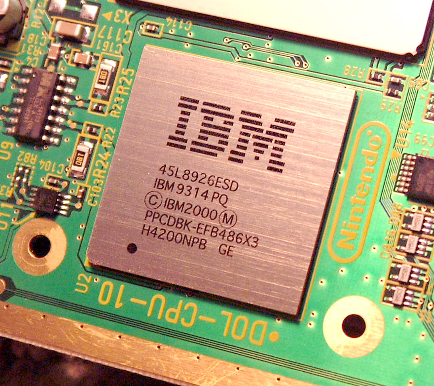
Gekko is a superscalar out-of-order 32-bit PowerPC microprocessor custom-made by IBM in 2000 for Nintendo to use as the CPU in their sixth generation game console, the GameCube, and later the Triforce Arcade Board.
Development
[edit]Gekko's role in the game system was to facilitate game scripting, artificial intelligence, physics and collision detection, custom graphics lighting effects and geometry such as smooth transformations, and moving graphics data through the system.
The project was announced in 1999 when IBM and Nintendo agreed to a $1 billion dollar contract (IBM's largest ever single order)[1] for a CPU running at approximately 400 MHz. IBM chose to modify their existing PowerPC 750CXe processor to suit Nintendo's needs, such as tight and balanced operation alongside the "Flipper" graphics processor. The customization was to the bus architecture, DMA, compression and floating point unit which support a special set of SIMD instructions. The CPU made ground work for custom lighting and geometry effects and could burst compressed data directly to the GPU.[citation needed]
The Gekko is considered to be the direct ancestor to the Broadway processor, also designed and manufactured by IBM, that powers the Wii console.
Features
[edit]- Customized PowerPC 750CXe core
- Clockrate – 486 MHz
- Superscalar Out-of-order execution
- 4 stages long two-integer ALUs (IU1 and IU2) – 32 bit
- 7 stages long Floating Point Unit – 64-bit double-precision FPU, usable as 2 × 32-bit SIMD for 1.9 single-precision GFLOPS performance using the Multiply–accumulate operation. The SIMD is often found under the denomination "paired singles."
- Branch Prediction Unit (BPU)
- Load-Store Unit (LSU)
- System Register Unit (SRU)
- Memory Management Unit (MMU)
- Branch Target Instruction Cache (BTIC)
- SIMD Instructions – PowerPC750 + roughly 50 new SIMD instructions, geared toward 3D graphics
- Front-side Bus – 64-bit enhanced 60x bus to GPU/chipset at 162 MHz clock with 1.3 GB/s peak bandwidth
- On-chip Cache – 64 KB 8-way associative L1 cache (32/32 KB instruction/data). 256 KB on-die, 2-way associative L2 cache
- DMIPS – 1125 (dhrystone 2.1)
- 180 nm IBM six-layer, copper-wire process. 43 mm² die
- 1.8 V for logic and I/O. 4.9 W dissipation
- 27 × 27 mm PBGA package with 256 contacts
- 6.35 million logic transistors and 18.6 million transistors total
See also
[edit]- Broadway (microprocessor), the processor in the Wii
- MIPS R4300, the processor in the Nintendo 64
References
[edit]- ^ "DataStream" (PDF). Edge. No. 79 (December 1999). 24 November 1999. p. 132.
- "IBM, Nintendo Announce $1 Billion Technology Agreement" (Press release). IBM. May 12, 1999. Archived from the original on 2006-08-21.
- A PowerPC compatible processor supporting high-performance 3-D graphics
| Hardware | |
|---|---|
| Accessories | |
| Games | |
| Emulators | |
| Related | |
| |
Gekko (processor)
View on GrokipediaOverview
General characteristics
The Gekko is a 32-bit superscalar, out-of-order PowerPC microprocessor custom-designed by IBM as a derivative of the PowerPC 750 architecture, with enhancements optimized for floating-point performance, data transfer efficiency, and graphics-oriented applications in gaming systems.[1][2] Developed in collaboration with Nintendo, it was introduced in 2000 specifically for the company's sixth-generation video game console.[5][2] The processor operates at a clock speed of 485 MHz and is fabricated using a 180 nm CMOS copper interconnect process with six layers of metal.[2][5] It features a single-core design with approximately 21 million transistors and consumes 4.9 W of power at a 1.8 V supply under typical conditions.[6][2] The Gekko employs a Harvard architecture, including a 32 KB eight-way set-associative L1 instruction cache, a 32 KB eight-way set-associative L1 data cache (partitionable with 16 KB lockable), and a 256 KB two-way set-associative on-chip L2 cache running at full core speed.[1][2] Connectivity is provided via an enhanced 60x front-side bus with a 32-bit address path and 64-bit data path, operating at an effective 162 MHz double-data-rate clock (derived from an 81 MHz base frequency via a 6:1 core-to-bus ratio) to deliver 1.3 GB/s peak bandwidth to the system chipset and GPU.[1][2] The Gekko was produced until 2007, aligning with the end of manufacturing for the Nintendo GameCube console in which it served as the primary CPU.[5]Role in Nintendo systems
The Gekko processor served as the primary central processing unit (CPU) in the Nintendo GameCube, launched in 2001, where it managed core game logic, artificial intelligence (AI), physics simulations, collision detection, and scripting tasks essential for interactive gameplay.[4] Designed specifically for gaming workloads, Gekko's superscalar out-of-order execution enabled efficient handling of these complex operations in real-time environments.[4] Gekko was co-designed alongside the Flipper graphics processing unit (GPU) to form an optimized 3D graphics pipeline, facilitating direct data sharing for vertex processing through a fixed-length first-in, first-out (FIFO) buffer in main memory, which supported both direct and indirect vertex modes for streamlined rendering.[4] In the GameCube architecture, Gekko interfaced with 24 MB of 1T-SRAM main memory via a 64-bit Northbridge bus for primary data access and 16 MB of auxiliary RAM (ARAM) via direct memory access (DMA) for audio buffering and other secondary tasks, ensuring balanced performance across system components.[4] This integration contributed to the GameCube's ability to deliver high-performance gaming at a cost-effective price point of $199.95 at launch, making advanced console capabilities accessible to a broader audience without exceeding budget constraints.[7] Beyond home consoles, Gekko powered the Triforce arcade system board, a 2002 collaboration between Nintendo, Sega, and Namco, where it acted as the main CPU for arcade titles such as Mario Kart Arcade GP, adapting GameCube hardware for commercial gaming machines.[8]Development
IBM-Nintendo collaboration
In May 1999, IBM and Nintendo announced a multiyear, $1 billion joint development agreement for IBM to design and manufacture custom silicon for Nintendo's next-generation game console, codenamed Dolphin (later released as the GameCube).[9][10] This partnership marked a significant collaboration aimed at creating a high-performance processor tailored for gaming applications.[11] Under the agreement, IBM took primary responsibility for the design and fabrication of the processor, dubbed Gekko, while Nintendo provided input on optimizations specific to gaming workloads, particularly to enhance 3D graphics processing and achieve cost reductions for mass-market adoption.[12][13] The collaboration represented a strategic shift from Nintendo's previous reliance on NEC's VR4300 MIPS-based CPU, used in the Nintendo 64, to the PowerPC architecture for improved performance-per-watt efficiency suitable for console constraints.[12][14] Development of Gekko began in the late 1990s, with the project advancing through final stages by 2000 to align with the GameCube's launch in 2001.[15][16] The core strategic motivations were to deliver superior 3D graphics capabilities at low power consumption and reduced manufacturing costs, enabling Nintendo to compete effectively in the evolving video game market while targeting broad consumer accessibility.[9][14] The base architecture was derived from IBM's PowerPC 750CXe, customized under Nintendo's guidance for console-specific needs.[12]Modifications from PowerPC 750CXe
The Gekko processor, developed through the IBM-Nintendo collaboration to meet game-specific requirements, represents a customized derivative of the PowerPC 750CXe, with alterations primarily aimed at optimizing performance within the constraints of a consumer console environment.[1][4] A key modification was the reduction of the clock speed to 485 MHz, significantly lower than the 750CXe's potential of up to 600-700 MHz, to manage power consumption and thermal output suitable for the compact GameCube form factor.[1][17][18] This adjustment prioritized reliability and efficiency in a battery-free, enclosed system over maximum processing frequency.[4] Branch prediction in Gekko includes a 512-entry Branch History Table (BHT) supporting four-level prediction and a 64-entry Branch Target Instruction Cache (BTIC).[1] Out-of-order execution was also tweaked, retaining superscalar dispatch of up to three instructions per cycle but limiting out-of-order loads to one per cycle with a two-cycle latency on cache hits, which better handles graphics-oriented workloads while reducing complexity.[1][4] The system bus interface maintained the 750CXe's 64-bit data width and 32-bit address bus under the 60x protocol but incorporated gaming-specific optimizations, such as a no-DRTRY mode for faster load operations, an integrated DMA engine, and a write-gather pipe, enabling more efficient memory access for graphics data transfers at 162 MHz.[1][4] These changes supported burst transfers and address pipelining tailored to high-bandwidth demands in 3D rendering.[1] For floating-point operations, Gekko added custom support for paired-single precision arithmetic via a three-stage FPU and 50 new SIMD instructions (e.g., ps_add, ps_mul, psq_l), utilizing 32 floating-point registers to accelerate 3D transformations and vector math essential for gaming, which the standard 750CXe FPU lacked.[1][17] These instructions typically exhibit 3-4 cycle latencies, with division operations ranging from 11-33 cycles, providing a lightweight alternative to full vector units.[1] Cost-saving measures included simplifying the integer execution units, where the second unit (IU2) omits multiply and divide capabilities to streamline design, and configuring caches as 32 KB eight-way set-associative L1 (split instruction and data) with a 256 KB L2, including a lockable 16 KB portion of the L1 data cache as a fast scratchpad for critical game data.[1][4] Fabricated on a 180 nm process with a reduced die size of 43 mm², these adjustments lowered manufacturing costs while integrating power management features like doze, nap, and sleep modes, along with thermal assist unit (TAU) monitoring, to fit economically within the console's embedded constraints.[1]Architecture
Core and pipeline design
The Gekko processor utilizes a four-stage integer pipeline (fetch, dispatch, execute, complete), facilitating out-of-order execution and dispatch of up to two instructions per cycle (enabling up to three issues with branch folding).[1] This design enables efficient instruction flow in a superscalar architecture derived from the PowerPC 750CXe with targeted modifications for gaming workloads.[2] Gekko supports triple-issue superscalar execution, allowing up to three instructions per cycle through two integer units for arithmetic and logical operations, a dedicated branch unit, and a floating-point unit that also processes multimedia tasks.[2] The branch processing unit features dynamic prediction via a 512-entry branch history table with two-bit saturating counters, enabling four prediction states to minimize misprediction penalties and improve performance in branching-heavy code such as game loops.[1] This mechanism reduces pipeline stalls by speculatively executing predicted paths, with a 64-entry branch target instruction cache further accelerating resolution of taken branches.[2] The floating-point unit supports single-precision operations in a pipelined configuration, achieving a 3-cycle latency for multiply-add instructions to support rapid vector computations in 3D graphics.[19] The integer units handle 32-bit arithmetic and logical operations.[1]Memory and bus subsystem
The Gekko processor employs a Harvard architecture, featuring separate 32 KB instruction and data caches at the L1 level, both configured as 8-way set-associative with 32-byte cache lines.[1][5] The instruction cache supports non-blocking loads to maintain pipeline efficiency, while the data cache includes a 16 KB lockable portion that enables developers to reserve space for direct memory access operations, facilitating parallel data transfers without stalling the core.[2][1] A unified 256 KB L2 cache, also on-chip, operates at the core clock frequency and uses a 2-way set-associative organization with 32-byte lines and a write-back policy.[5][1] This cache integrates seamlessly with the L1 levels to provide hit-under-miss capabilities, reducing latency for subsequent accesses, and supports configurable coherency through bus snooping for multi-processor environments, though Gekko is typically deployed in single-core systems.[2][1] The front-side bus interface is 64 bits wide for data (with a 32-bit address bus) and runs at a base frequency of 81 MHz in double data rate (DDR) mode, achieving 162 MT/s and a peak bandwidth of 1.3 GB/s to main memory.[2][1] An integrated DMA controller enhances data handling with a 15-entry command queue, where each entry can initiate transfers of up to 4 KB in 32-byte increments between the locked L1 data cache and external memory, operating in parallel with CPU execution to minimize intervention.[2][1] Gekko supports a 1T-SRAM main memory interface tailored for the Nintendo GameCube, where the GameCube's 24 MB 1T-SRAM main memory and 16 MB auxiliary DRAM (ARAM) benefit from latency optimizations such as store gathering in a 128-byte write FIFO and critical double-word first forwarding to accelerate texture and graphics data loading.[2][5] These features, combined with the DMA's ability to bypass the core for transfers to the GPU and ARAM, enable efficient streaming of game assets without disrupting computational workloads.[2][1]Instruction set
Base PowerPC compatibility
The Gekko processor fully implements the PowerPC User Instruction Set Architecture (UISA) in 32-bit mode, encompassing the complete set of user-level instructions for integer arithmetic, floating-point operations, and load/store accesses. This includes standard integer instructions such as addition, multiplication, and logical operations, as well as load/store variants for byte, halfword, word, and doubleword data types. Floating-point instructions adhere to the IEEE 754 standard for single-precision arithmetic, supporting operations like addition, subtraction, multiplication, and division through a dedicated floating-point unit (FPU). The architecture provides 32 general-purpose registers (GPRs), each 32 bits wide, for integer computations, along with 32 floating-point registers (FPRs), each 64 bits wide to accommodate single- or double-precision formats.[1][2] Gekko complies with the PowerPC Virtual Environment Architecture (VEA), which defines facilities for cache management, time base operations, and a multiprocessor memory consistency model to ensure reliable virtual addressing and synchronization. This compliance enables standard handling of cache instructions and time base facilities, facilitating efficient memory access patterns in embedded environments. Additionally, the processor supports the PowerPC Embedded Application Binary Interface (EABI), which standardizes data representation, calling conventions, and memory layout, allowing compatibility with conventional compiler toolchains and software development environments for PowerPC-based systems.[1] For control flow, Gekko incorporates the full suite of branch instructions and condition register (CR) operations defined in the UISA, including unconditional branches (b), conditional branches (bc), and branch-to-register variants (bclr, bcctr) that utilize the link register (LR) and count register (CTR). The CR, a 32-bit register divided into eight 4-bit fields, supports logical operations such as crand and cror for condition code manipulation, enabling precise branching decisions based on comparison results from integer or floating-point instructions. While these core mechanisms align with standard PowerPC features, Gekko includes minor extensions for multimedia processing that build upon this foundation. Exception handling and memory management further align with PowerPC conventions through VEA-defined synchronization primitives, ensuring ordered execution in virtual environments.[1][2]
Custom SIMD extensions
The Gekko processor extends the PowerPC architecture with custom Single Instruction, Multiple Data (SIMD) capabilities through its Paired Singles (PS) mode, which treats each 64-bit floating-point register (FPR) as two independent 32-bit single-precision floating-point values—denoted as PS0 (upper 32 bits) and PS1 (lower 32 bits)—enabling parallel vector operations optimized for 3D graphics workloads.[1] This mode is activated by setting the PSE bit in the HID2 register, allowing the floating-point unit (FPU) to execute two single-precision operations per cycle while maintaining compatibility with double-precision instructions, which execute normally using the full 64 bits.[1][3] The design supports a peak throughput of 1.9 GFLOPS, with full pipelining and reservation stations to handle fused multiply-add operations efficiently for tasks like lighting and geometry transformations.[2] In PS mode, core arithmetic instructions perform parallel computations on both PS0 and PS1 elements simultaneously; for example,ps_add adds corresponding pairs from source registers frA and frB, storing the results in frD, while ps_madd executes a fused multiply-add (frA × frC + frB) across both pairs in a single cycle, facilitating vector dot products and matrix multiplications common in 3D rendering.[1] Additional variants like ps_msub, ps_nmadd, and ps_nmsub provide negated and subtractive forms for flexible expression evaluation, with ps_div handling parallel division over longer latencies (17 cycles).[1] These operations leverage the FPSCR for rounding control and exception handling, ensuring precise control over floating-point behavior in game engines.[1]
Gekko incorporates 16 custom instructions dedicated to vertex data packing and unpacking, primarily through quantized load and store operations that convert between fixed-point integers and floating-point values, reducing memory bandwidth demands for graphics data.[2] The psq_l family (including psq_l, psq_lu, psq_lx, and psq_lux) loads 8- or 16-bit signed/unsigned integers from memory, applies scaling factors defined in General Quantized Registers (GQR0–GQR7) for normalization, and converts them to paired single-precision floats in an FPR, enabling efficient ingestion of compressed vertex attributes like positions or normals.[1] Complementing these, the psq_st variants (psq_st, psq_stu, psq_stx, and psq_stux) perform the reverse: extracting paired singles from an FPR, quantizing them back to 8- or 16-bit integers with GQR-specified scaling, and storing them, achieving 2:1 or 4:1 data compression ratios that effectively boost bus bandwidth to 5.2 GB/s for texture and geometry handling.[2][1] These instructions, totaling eight load and eight store forms when accounting for addressing modes, streamline vertex processing pipelines by minimizing conversion overhead.[1]
For matrix transformations and vector swizzling in 3D lighting calculations, Gekko provides specialized merge instructions such as ps_merge00, ps_merge01, ps_merge10, and ps_merge11, which recombine PS0 and PS1 elements from two source FPRs into a destination register to rearrange vector components without additional arithmetic, supporting operations like coordinate system rotations or normal vector interpolation.[1] Related sum instructions, including ps_sum0 (adding PS0 from frA to PS1 from frB) and ps_sum1 (adding PS1 from frA to PS0 from frB), enable cross-lane accumulation for dot products, further accelerating graphics math.[1]
Data compression is further enhanced by instructions like stvewx (store vector element word indexed), which selectively stores a 32-bit word from an FPR's lower bits to memory using indexed addressing, allowing precise placement of vector elements in buffers for efficient texture coordinate packing or geometry streaming.[1] Optimizations for fixed-point to floating-point conversions are integral to these extensions, particularly via the quantized loads that use GQR scaling to map low-precision integers (e.g., 16-bit fixed-point vertices) directly into normalized floats, avoiding explicit conversion instructions and reducing cycles in graphics pipelines.[2][1] These features collectively integrate with the Flipper GPU for shared vertex processing in Nintendo systems.[2]