Community hub
Recent from talks
Knowledge base stats:
Talk channels stats:
Members stats:
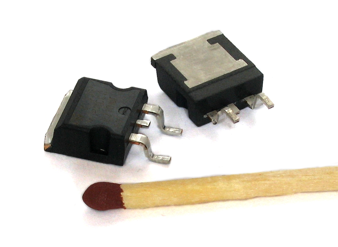
Power MOSFET
A power MOSFET is a type of metal–oxide–semiconductor field-effect transistor (MOSFET) designed to handle significant power levels. Compared to the other power semiconductor devices, such as an insulated-gate bipolar transistor (IGBT) or a thyristor, its main advantages are high switching speed and good efficiency at low voltages. It shares with the IGBT an isolated gate that makes it easy to drive. They can exhibit low gain, sometimes to the extent that the gate voltage needs to be higher than the voltage being controlled.
The design of power MOSFETs was made possible by the evolution of MOSFET and CMOS technology, used for manufacturing integrated circuits since the 1960s. The power MOSFET shares its operating principle with its low-power counterpart, the lateral MOSFET. The power MOSFET, which is commonly used in power electronics, was adapted from the standard MOSFET and commercially introduced in the 1970s.
The power MOSFET is the most common power semiconductor device in the world, due to its low gate drive power, fast switching speed, easy advanced paralleling capability, wide bandwidth, ruggedness, easy drive, simple biasing, ease of application, and ease of repair. In particular, it is the most widely used low-voltage (less than 200 V) switch. It can be found in a wide range of applications, such as most power supplies, DC-to-DC converters, low-voltage motor controllers, and many other applications.
The MOSFET was invented at Bell Labs between 1955 and 1960. It was a breakthrough in power electronics. Generations of MOSFETs enabled power designers to achieve performance and density levels not possible with bipolar transistors.
In 1969, Hitachi introduced the first vertical power MOSFET, which would later be known as the VMOS (V-groove MOSFET). The same year, the DMOS (double-diffused MOSFET) with self-aligned gate was first reported by Y. Tarui, Y. Hayashi and Toshihiro Sekigawa of the Electrotechnical Laboratory (ETL). In 1974, Jun-ichi Nishizawa at Tohoku University invented a power MOSFET for audio, which was soon manufactured by Yamaha Corporation for their high fidelity audio amplifiers. JVC, Pioneer Corporation, Sony and Toshiba also began manufacturing amplifiers with power MOSFETs in 1974. Siliconix commercially introduced a VMOS in 1975.
The VMOS and DMOS developed into what has become known as VDMOS (vertical DMOS). John Moll's research team at HP Labs fabricated DMOS prototypes in 1977, and demonstrated advantages over the VMOS, including lower on-resistance and higher breakdown voltage. The same year, Hitachi introduced the LDMOS (lateral DMOS), a planar type of DMOS. Hitachi was the only LDMOS manufacturer between 1977 and 1983, during which time LDMOS was used in audio power amplifiers from manufacturers such as HH Electronics (V-series) and Ashly Audio, and were used for music and public address systems. With the introduction of the 2G digital mobile network in 1995, the LDMOS became the most widely used RF power amplifier in mobile networks such as 2G, 3G, and 4G.
Alex Lidow co-invented the HexFET, a hexagonal type of Power MOSFET, at Stanford University in 1977, along with Tom Herman. The HexFET was commercialized by International Rectifier in 1978. The insulated-gate bipolar transistor (IGBT), which combines elements of both the power MOSFET and the bipolar junction transistor (BJT), was developed by Jayant Baliga at General Electric between 1977 and 1979.
The superjunction MOSFET is a type of power MOSFET that uses P+ columns that penetrate the N− epitaxial layer. The idea of stacking P and N layers was first proposed by Shozo Shirota and Shigeo Kaneda at Osaka University in 1978. David J. Coe at Philips invented the superjunction MOSFET with alternating p-type and n-type layers, for which a US patent was awarded in 1988.
Hub AI
Power MOSFET AI simulator
(@Power MOSFET_simulator)
Power MOSFET
A power MOSFET is a type of metal–oxide–semiconductor field-effect transistor (MOSFET) designed to handle significant power levels. Compared to the other power semiconductor devices, such as an insulated-gate bipolar transistor (IGBT) or a thyristor, its main advantages are high switching speed and good efficiency at low voltages. It shares with the IGBT an isolated gate that makes it easy to drive. They can exhibit low gain, sometimes to the extent that the gate voltage needs to be higher than the voltage being controlled.
The design of power MOSFETs was made possible by the evolution of MOSFET and CMOS technology, used for manufacturing integrated circuits since the 1960s. The power MOSFET shares its operating principle with its low-power counterpart, the lateral MOSFET. The power MOSFET, which is commonly used in power electronics, was adapted from the standard MOSFET and commercially introduced in the 1970s.
The power MOSFET is the most common power semiconductor device in the world, due to its low gate drive power, fast switching speed, easy advanced paralleling capability, wide bandwidth, ruggedness, easy drive, simple biasing, ease of application, and ease of repair. In particular, it is the most widely used low-voltage (less than 200 V) switch. It can be found in a wide range of applications, such as most power supplies, DC-to-DC converters, low-voltage motor controllers, and many other applications.
The MOSFET was invented at Bell Labs between 1955 and 1960. It was a breakthrough in power electronics. Generations of MOSFETs enabled power designers to achieve performance and density levels not possible with bipolar transistors.
In 1969, Hitachi introduced the first vertical power MOSFET, which would later be known as the VMOS (V-groove MOSFET). The same year, the DMOS (double-diffused MOSFET) with self-aligned gate was first reported by Y. Tarui, Y. Hayashi and Toshihiro Sekigawa of the Electrotechnical Laboratory (ETL). In 1974, Jun-ichi Nishizawa at Tohoku University invented a power MOSFET for audio, which was soon manufactured by Yamaha Corporation for their high fidelity audio amplifiers. JVC, Pioneer Corporation, Sony and Toshiba also began manufacturing amplifiers with power MOSFETs in 1974. Siliconix commercially introduced a VMOS in 1975.
The VMOS and DMOS developed into what has become known as VDMOS (vertical DMOS). John Moll's research team at HP Labs fabricated DMOS prototypes in 1977, and demonstrated advantages over the VMOS, including lower on-resistance and higher breakdown voltage. The same year, Hitachi introduced the LDMOS (lateral DMOS), a planar type of DMOS. Hitachi was the only LDMOS manufacturer between 1977 and 1983, during which time LDMOS was used in audio power amplifiers from manufacturers such as HH Electronics (V-series) and Ashly Audio, and were used for music and public address systems. With the introduction of the 2G digital mobile network in 1995, the LDMOS became the most widely used RF power amplifier in mobile networks such as 2G, 3G, and 4G.
Alex Lidow co-invented the HexFET, a hexagonal type of Power MOSFET, at Stanford University in 1977, along with Tom Herman. The HexFET was commercialized by International Rectifier in 1978. The insulated-gate bipolar transistor (IGBT), which combines elements of both the power MOSFET and the bipolar junction transistor (BJT), was developed by Jayant Baliga at General Electric between 1977 and 1979.
The superjunction MOSFET is a type of power MOSFET that uses P+ columns that penetrate the N− epitaxial layer. The idea of stacking P and N layers was first proposed by Shozo Shirota and Shigeo Kaneda at Osaka University in 1978. David J. Coe at Philips invented the superjunction MOSFET with alternating p-type and n-type layers, for which a US patent was awarded in 1988.