Community hub
Recent from talks
Knowledge base stats:
Talk channels stats:
Members stats:
Multigate device
A multigate device, multi-gate MOSFET or multi-gate field-effect transistor (MuGFET) refers to a metal–oxide–semiconductor field-effect transistor (MOSFET) that has more than one gate on a single transistor. The multiple gates may be controlled by a single gate electrode, wherein the multiple gate surfaces act electrically as a single gate, or by independent gate electrodes. A multigate device employing independent gate electrodes is sometimes called a multiple-independent-gate field-effect transistor (MIGFET). The most widely used multi-gate devices are the FinFET (fin field-effect transistor) and the GAAFET (gate-all-around field-effect transistor), which are non-planar transistors, or 3D transistors.
Multi-gate transistors are one of the several strategies being developed by MOS semiconductor manufacturers to create ever-smaller microprocessors and memory cells, colloquially referred to as extending Moore's law (in its narrow, specific version concerning density scaling, exclusive of its careless historical conflation with Dennard scaling). Development efforts into multigate transistors have been reported by the Electrotechnical Laboratory, Toshiba, Grenoble INP, Hitachi, IBM, TSMC, UC Berkeley, Infineon Technologies, Intel, AMD, Samsung Electronics, KAIST, Freescale Semiconductor, and others, and the ITRS predicted correctly that such devices will be the cornerstone of sub-32 nm technologies. The primary roadblock to widespread implementation is manufacturability, as both planar and non-planar designs present significant challenges, especially with respect to lithography and patterning. Other complementary strategies for device scaling include channel strain engineering, silicon-on-insulator-based technologies, and high-κ/metal gate materials.
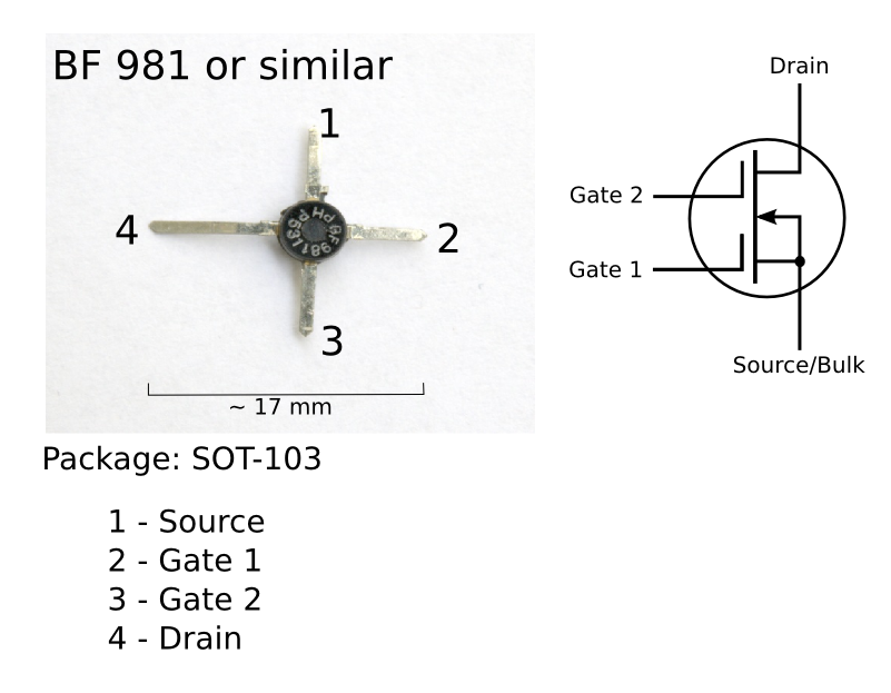
Dual-gate MOSFETs are commonly used in very high frequency (VHF) mixers and in sensitive VHF front-end amplifiers. They are available from manufacturers such as Motorola, NXP Semiconductors, and Hitachi.
Dozens of multigate transistor variants may be found in the literature. In general, these variants may be differentiated and classified in terms of architecture (planar vs. non-planar design) and the number of channels/gates (2, 3, or 4).
A planar double-gate MOSFET (DGMOS) employs conventional planar (layer-by-layer) manufacturing processes to create double-gate MOSFET (metal–oxide–semiconductor field-effect transistor) devices, avoiding more stringent lithography requirements associated with non-planar, vertical transistor structures. In planar double-gate transistors the drain–source channel is sandwiched between two independently fabricated gate/gate-oxide stacks. The primary challenge in fabricating such structures is achieving satisfactory self-alignment between the upper and lower gates.
FlexFET is a planar, independently double-gated transistor with a damascene metal top gate MOSFET and an implanted JFET bottom gate that are self-aligned in a gate trench. This device is highly scalable due to its sub-lithographic channel length; non-implanted ultra-shallow source and drain extensions; non-epi raised source and drain regions; and gate-last flow. FlexFET is a true double-gate transistor in that (1) both the top and bottom gates provide transistor operation, and (2) the operation of the gates is coupled such that the top gate operation affects the bottom gate operation and vice versa. FlexFET was developed and is manufactured by American Semiconductor, Inc.
FinFET (fin field-effect transistor) is a type of non-planar transistor, or "3D" transistor (not to be confused with 3D microchips). The FinFET is a variation on traditional MOSFETs distinguished by the presence of a thin silicon "fin" inversion channel on top of the substrate, allowing the gate to make two points of contact: the left and right sides of the fin. The thickness of the fin (measured in the direction from source to drain) determines the effective channel length of the device. The wrap-around gate structure provides a better electrical control over the channel and thus helps in reducing the leakage current and overcoming other short-channel effects.
The first FinFET transistor type was called a depleted lean-channel transistor or "DELTA" transistor, which was first fabricated by Hitachi Central Research Laboratory's Digh Hisamoto, Toru Kaga, Yoshifumi Kawamoto and Eiji Takeda in 1989. In the late 1990s, Digh Hisamoto began collaborating with an international team of researchers on further developing DELTA technology, including TSMC's Chenming Hu and a UC Berkeley research team including Tsu-Jae King Liu, Jeffrey Bokor, Xuejue Huang, Leland Chang, Nick Lindert, S. Ahmed, Cyrus Tabery, Yang-Kyu Choi, Pushkar Ranade, Sriram Balasubramanian, A. Agarwal and M. Ameen. In 1998, the team developed the first N-channel FinFETs and successfully fabricated devices down to a 17 nm process. The following year, they developed the first P-channel FinFETs. They coined the term "FinFET" (fin field-effect transistor) in a December 2000 paper.
Hub AI
Multigate device AI simulator
(@Multigate device_simulator)
Multigate device
A multigate device, multi-gate MOSFET or multi-gate field-effect transistor (MuGFET) refers to a metal–oxide–semiconductor field-effect transistor (MOSFET) that has more than one gate on a single transistor. The multiple gates may be controlled by a single gate electrode, wherein the multiple gate surfaces act electrically as a single gate, or by independent gate electrodes. A multigate device employing independent gate electrodes is sometimes called a multiple-independent-gate field-effect transistor (MIGFET). The most widely used multi-gate devices are the FinFET (fin field-effect transistor) and the GAAFET (gate-all-around field-effect transistor), which are non-planar transistors, or 3D transistors.
Multi-gate transistors are one of the several strategies being developed by MOS semiconductor manufacturers to create ever-smaller microprocessors and memory cells, colloquially referred to as extending Moore's law (in its narrow, specific version concerning density scaling, exclusive of its careless historical conflation with Dennard scaling). Development efforts into multigate transistors have been reported by the Electrotechnical Laboratory, Toshiba, Grenoble INP, Hitachi, IBM, TSMC, UC Berkeley, Infineon Technologies, Intel, AMD, Samsung Electronics, KAIST, Freescale Semiconductor, and others, and the ITRS predicted correctly that such devices will be the cornerstone of sub-32 nm technologies. The primary roadblock to widespread implementation is manufacturability, as both planar and non-planar designs present significant challenges, especially with respect to lithography and patterning. Other complementary strategies for device scaling include channel strain engineering, silicon-on-insulator-based technologies, and high-κ/metal gate materials.
Dual-gate MOSFETs are commonly used in very high frequency (VHF) mixers and in sensitive VHF front-end amplifiers. They are available from manufacturers such as Motorola, NXP Semiconductors, and Hitachi.
Dozens of multigate transistor variants may be found in the literature. In general, these variants may be differentiated and classified in terms of architecture (planar vs. non-planar design) and the number of channels/gates (2, 3, or 4).
A planar double-gate MOSFET (DGMOS) employs conventional planar (layer-by-layer) manufacturing processes to create double-gate MOSFET (metal–oxide–semiconductor field-effect transistor) devices, avoiding more stringent lithography requirements associated with non-planar, vertical transistor structures. In planar double-gate transistors the drain–source channel is sandwiched between two independently fabricated gate/gate-oxide stacks. The primary challenge in fabricating such structures is achieving satisfactory self-alignment between the upper and lower gates.
FlexFET is a planar, independently double-gated transistor with a damascene metal top gate MOSFET and an implanted JFET bottom gate that are self-aligned in a gate trench. This device is highly scalable due to its sub-lithographic channel length; non-implanted ultra-shallow source and drain extensions; non-epi raised source and drain regions; and gate-last flow. FlexFET is a true double-gate transistor in that (1) both the top and bottom gates provide transistor operation, and (2) the operation of the gates is coupled such that the top gate operation affects the bottom gate operation and vice versa. FlexFET was developed and is manufactured by American Semiconductor, Inc.
FinFET (fin field-effect transistor) is a type of non-planar transistor, or "3D" transistor (not to be confused with 3D microchips). The FinFET is a variation on traditional MOSFETs distinguished by the presence of a thin silicon "fin" inversion channel on top of the substrate, allowing the gate to make two points of contact: the left and right sides of the fin. The thickness of the fin (measured in the direction from source to drain) determines the effective channel length of the device. The wrap-around gate structure provides a better electrical control over the channel and thus helps in reducing the leakage current and overcoming other short-channel effects.
The first FinFET transistor type was called a depleted lean-channel transistor or "DELTA" transistor, which was first fabricated by Hitachi Central Research Laboratory's Digh Hisamoto, Toru Kaga, Yoshifumi Kawamoto and Eiji Takeda in 1989. In the late 1990s, Digh Hisamoto began collaborating with an international team of researchers on further developing DELTA technology, including TSMC's Chenming Hu and a UC Berkeley research team including Tsu-Jae King Liu, Jeffrey Bokor, Xuejue Huang, Leland Chang, Nick Lindert, S. Ahmed, Cyrus Tabery, Yang-Kyu Choi, Pushkar Ranade, Sriram Balasubramanian, A. Agarwal and M. Ameen. In 1998, the team developed the first N-channel FinFETs and successfully fabricated devices down to a 17 nm process. The following year, they developed the first P-channel FinFETs. They coined the term "FinFET" (fin field-effect transistor) in a December 2000 paper.