
Community hub
Pin grid array
View on WikipediaThis article needs additional citations for verification. (December 2011) |
_CPU-pins_PNr%C2%B00295.jpg)

.JPG)
A pin grid array (PGA) is a type of integrated circuit packaging. In a PGA, the package is square or rectangular, and the pins are arranged in a regular array on the underside of the package. The pins are commonly spaced 2.54 mm (0.1") apart,[1] and may or may not cover the entire underside of the package. 1.27 mm (0.05") is commonly used with higher pin count PGAs.
PGAs are often mounted on printed circuit boards using the through hole method or inserted into a socket. PGAs allow for more pins per integrated circuit than older packages, such as dual in-line package (DIP).
Chip mounting
[edit]
The chip can be mounted either on the top or the bottom (the pinned side). Connections can be made either by wire bonding or through flip chip mounting. Typically, PGA packages use wire bonding when the chip is mounted on the pinned side, and flip chip construction when the chip is on the top side. Some PGA packages contain multiple dies, for example Zen 2 and Zen 3 Ryzen CPUs for the AM4 socket.
Flip chip
[edit]
A flip-chip pin grid array (FC-PGA or FCPGA) is a form of pin grid array in which the die faces downwards on the top of the substrate with the back of the die exposed. This allows the die to have a more direct contact with the heatsink or other cooling mechanism.
FC-PGA CPUs were introduced by Intel in 1999, for Coppermine core Pentium III and Celeron[2] processors based on Socket 370, and were produced until Socket G3 in 2013. FC-PGA processors fit into zero insertion force (ZIF) motherboard sockets; similar packages were also used by AMD.
Material
[edit]Ceramic
[edit]A ceramic pin grid array (CPGA) is a type of packaging used by integrated circuits. This type of packaging uses a ceramic substrate with pins arranged in a pin grid array. Some CPUs that use CPGA packaging are the AMD Socket A Athlons and the Duron.
A CPGA was used by AMD for Athlon and Duron processors based on Socket A, as well as some AMD processors based on Socket AM2 and Socket AM2+. While similar form factors have been used by other manufacturers, they are not officially referred to as CPGA. This type of packaging uses a ceramic substrate with pins arranged in an array.
-
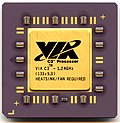 A 1.2 GHz VIA C3 microprocessor in a ceramic package
 -
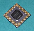 133 MHz Pentium chip in a ceramic package


Organic
[edit]An organic pin grid array (OPGA) is a type of connection for integrated circuits, and especially CPUs, where the silicon die is attached to a plate made out of an organic plastic which is pierced by an array of pins which make the requisite connections to the socket.
-
 The underside of a Celeron-400 in a PPGA
 -
 An OPGA CPU. Note the brown color – many OPGA parts are colored green. The die is in the center of the device, and the four gray circles are foam spacers to relieve pressure from the die, caused by the heat sink.


Plastic
[edit]
Plastic pin grid array (PPGA) packaging was used by Intel for late-model Mendocino core Celeron processors based on Socket 370.[3] Some pre-Socket 8 processors also used a similar form factor, although they were not officially referred to as PPGA.

Pin layout
[edit]Staggered pin
[edit]The staggered pin grid array (SPGA) is used by Intel processors based on Socket 5 and Socket 7. Socket 8 used a partial SPGA layout on half the processor.


It consists of two square arrays of pins, offset in both directions by half the minimum distance between pins in one of the arrays. Put differently: within a square boundary the pins form a diagonal square lattice. There is generally a section in the center of the package without any pins. SPGA packages are usually used by devices that require a higher pin density than what a PGA can provide, such as microprocessors.
Stud
[edit]A stud grid array (SGA) is a short-pinned pin grid array chip scale package for use in surface-mount technology. The polymer stud grid array or plastic stud grid array was developed jointly by the Interuniversity Microelectronics Centre (IMEC) and Laboratory for Production Technology, Siemens.[4][5]
rPGA
[edit]The reduced pin grid array was used by the socketed mobile variants of Intel's Core i3/5/7 processors and features a reduced pin pitch of 1 mm,[6] as opposed to the 1.27 mm pin pitch used by contemporary AMD processors and older Intel processors. It is used in the G1, G2, and G3 sockets.
See also
[edit]- Ball grid array (BGA)
- Centered square number
- Chip carrier - chip packaging and package types list
- Dual in-line package (DIP)
- Land grid array (LGA)
- Single in-line package (SIP)
- Zig-zag in-line package (ZIP)
References
[edit]- ^ Vijay Nath (24 March 2017). Proceedings of the International Conference on Nano-electronics, Circuits & Communication Systems. Springer. p. 304. ISBN 978-981-10-2999-8.
- ^ "Intel Releases New Design for sub-$1,000 PCs". Philippine Daily Inquirer. April 24, 2000.
{{cite web}}: Missing or empty|url=(help) - ^ Robert Bruce Thompson; Barbara Fritchman Thompson (24 July 2003). PC Hardware in a Nutshell: A Desktop Quick Reference. O'Reilly Media, Inc. p. 44. ISBN 978-0-596-55234-3.
- ^ "BGA socket/BGA 소켓". Jsits.com. Retrieved 2015-06-05.
- ^ link (in German) Archived October 1, 2011, at the Wayback Machine
- ^ "Molex Sockets for Servers, Desktops and Notebooks Earn Intel® Validation". Archived from the original on 2019-12-09. Retrieved 2016-03-15.
Sources
[edit]- Thomas, Andrew (August 4, 2010). "What the Hell is… a flip-chip?". The Register. Retrieved December 30, 2011.
- "XSERIES 335 XEON DP-2.4G 512 MB". CNET. October 26, 2002. Retrieved December 30, 2011.
- "SURFACE MOUNT NOMENCLATURE AND PACKAGING" (PDF).
External links
[edit]- Intel CPU Processor Identification
- Ball Grid Arrays: the High-Pincount Workhorses[permanent dead link], John Baliga, associate editor, Semiconductor International, 9/1/1999
- Spot on component packaging[permanent dead link], 08/1998, Elektronik, Produktion & Prüftechnik
- Terminology