
Community hub
Recent from talks
Contribute something
Nothing was collected or created yet.
x87 is a floating-point-related subset of the x86 architecture instruction set. It originated as an extension of the 8086 instruction set in the form of optional floating-point coprocessors (FPU) that work in tandem with corresponding x86 CPUs. These microchips have names ending in "87". This is also known as the NPX (numeric processor extension). Like other extensions to the basic instruction set, x87 instructions are not strictly needed to construct working programs, but provide hardware and microcode implementations of common numerical tasks, allowing these tasks to be performed much faster than corresponding machine code routines can. The x87 instruction set includes instructions for basic floating-point operations such as addition, subtraction and comparison, but also for more complex numerical operations, such as the computation of the tangent function and its inverse, for example.
Most x86 processors since the Intel 80486 have had these x87 instructions implemented in the main CPU, but the term is sometimes still used to refer to that part of the instruction set. Before x87 instructions were standard in PCs, compilers or programmers had to use rather slow library calls to perform floating-point operations, a method that is still common in (low-cost) embedded systems.
Description
[edit]The x87 registers form an eight-level deep non-strict stack structure ranging from ST(0) to ST(7) with registers that can be directly accessed by either operand, using an offset relative to the top, as well as pushed and popped. (This scheme may be compared to how a stack frame may be both pushed/popped and indexed.)
There are instructions to push, calculate, and pop values on top of this stack; unary operations (FSQRT, FPTAN etc.) then implicitly address the topmost ST(0), while binary operations (FADD, FMUL, FCOM, etc.) implicitly address ST(0) and ST(1). The non-strict stack model also allows binary operations to use ST(0) together with a direct memory operand or with an explicitly specified stack register, ST(x), in a role similar to a traditional accumulator (a combined destination and left operand). This can also be reversed on an instruction-by-instruction basis with ST(0) as the unmodified operand and ST(x) as the destination. Furthermore, the contents in ST(0) can be exchanged with another stack register using an instruction called FXCH ST(x).
These properties make the x87 stack usable as seven freely addressable registers plus a dedicated accumulator (or as seven independent accumulators). This is especially applicable on superscalar x86 processors (such as the Pentium of 1993 and later), where these exchange instructions (codes D9C8..D9CFh) are optimized down to a zero clock penalty by using one of the integer paths for FXCH ST(x) in parallel with the FPU instruction. Despite being natural and convenient for human assembly language programmers, some compiler writers have found it complicated to construct automatic code generators that schedule x87 code effectively. Such a stack-based interface potentially can minimize the need to save scratch variables in function calls compared with a register-based interface[1] (although, historically, design issues in the 8087 implementation limited that potential.[2][3])
The x87 provides single-precision, double-precision and 80-bit double-extended precision binary floating-point arithmetic as per the IEEE 754-1985 standard. By default, the x87 processors all use 80-bit double-extended precision internally (to allow sustained precision over many calculations, see IEEE 754 design rationale). A given sequence of arithmetic operations may thus behave slightly differently compared to a strict single-precision or double-precision IEEE 754 FPU.[4] As this may sometimes be problematic for some semi-numerical calculations written to assume double precision for correct operation, to avoid such problems, the x87 can be configured using a special configuration/status register to automatically round to single or double precision after each operation. Since the introduction of SSE2, the x87 instructions are not as essential as they once were, but remain important as a high-precision scalar unit for numerical calculations sensitive to round-off error and requiring the 64-bit mantissa precision and extended range available in the 80-bit format.
Performance
[edit]Clock cycle counts for examples of typical x87 FPU instructions (only register-register versions shown here).[5]
The A...B notation (minimum to maximum) covers timing variations dependent on transient pipeline status and the arithmetic precision chosen (32, 64 or 80 bits); it also includes variations due to numerical cases (such as the number of set bits, zero, etc.). The L → H notation depicts values corresponding to the lowest (L) and the highest (H) maximal clock frequencies that were available.
| x87 implementation | FADD | FMUL | FDIV | FXCH | FCOM | FSQRT | FPTAN | FPATAN | Max clock (MHz) |
Peak FMUL (millions/s) |
FMUL§ rel. 5 MHz 8087 |
|---|---|---|---|---|---|---|---|---|---|---|---|
| 8087 | 70…100 | 90…145 | 193…203 | 10…15 | 40…50 | 180…186 | 30…540 | 250…800 | 5 → 10 | 0.034…0.055 → 0.100…0.111 | 1 → 2× as fast |
| 80287 (original) | 6 → 12 | 0.041…0.066 → 0.083…0.133 | 1.2 → 2.4× | ||||||||
| 80387 (and later 287 models) | 23…34 | 29…57 | 88…91 | 18 | 24 | 122…129 | 191…497 | 314…487 | 16 → 33 | 0.280…0.552 → 0.580…1.1 | ~10 → 20× |
| 80486 (or 80487) | 8…20 | 16 | 73 | 4 | 4 | 83…87 | 200…273 | 218…303 | 16 → 50 | 1.0 → 3.1 | ~18 → 56× |
| Cyrix 6x86, Cyrix MII | 4…7 | 4…6 | 24…34 | 2 | 4 | 59…60 | 117…129 | 97…161 | 66 → 300 | 11…16 → 50…75 | ~320 → 1400× |
| AMD K6 (including K6 II/III) | 2 | 2 | 21…41 | 2 | 3 | 21…41 | ? | ? | 166 → 550 | 83 → 275 | ~1500 → 5000× |
| Pentium / Pentium MMX | 1…3 | 1…3 | 39 | 1 (0*) | 1…4 | 70 | 17…173 | 19…134 | 60 → 300 | 20…60 → 100…300 | ~1100 → 5400× |
| Pentium Pro | 1…3 | 2…5 | 16…56 | 1 | 28…68 | ? | ? | 150 → 200 | 30…75 → 40…100 | ~1400 → 1800× | |
| Pentium II / III | 1…3 | 2…5 | 17…38 | 1 | 27…50 | ? | ? | 233 → 1400 | 47…116 → 280…700 | ~2100 → 13000× | |
| Athlon (K7) | 1…4 | 1…4 | 13…24 | 1…2 | 16…35 | ? | ? | 500 → 2330 | 125…500 → 580…2330 | ~9000 → 42000× | |
| Athlon 64 (K8) | 1000 → 3200 | 250…1000 → 800…3200 | ~18000 → 58000× | ||||||||
| Pentium 4 | 1…5 | 2…7 | 20…43 | multiple cycles |
1 | 20…43 | ? | ? | 1300 → 3800 | 186…650 → 543…1900 | ~11000 → 34000× |
- * An effective zero clock delay is often possible, via superscalar execution.
- § The 5 MHz 8087 was the original x87 processor. Compared to typical software-implemented floating-point routines on an 8086 (without an 8087), the factors would be even larger, perhaps by another factor of 10 (i.e., a correct floating-point addition in assembly language may well consume over 1000 cycles).
Manufacturers
[edit]Companies that have designed or manufactured[a] floating-point units compatible with the Intel 8087 or later models include AMD (287, 387, 486DX, 5x86, K5, K6, K7, K8), Chips and Technologies (the Super MATH coprocessors), Cyrix (the FasMath, Cx87SLC, Cx87DLC, etc., 6x86, Cyrix MII), Fujitsu (early Pentium Mobile etc.), Harris Semiconductor (manufactured 80387 and 486DX processors), IBM (various 387 and 486 designs), IDT (the WinChip, C3, C7, Nano, etc.), IIT (the 2C87, 3C87, etc.), LC Technology (the Green MATH coprocessors), National Semiconductor (the Geode GX1, Geode GXm, etc.), NexGen (the Nx587), Rise Technology (the mP6), ST Microelectronics (manufactured 486DX, 5x86, etc.), Texas Instruments (manufactured 486DX processors etc.), Transmeta (the TM5600 and TM5800), ULSI (the Math·Co coprocessors), VIA (the C3, C7, and Nano, etc.), Weitek (the 1067, 1167, 3167 and 4167), and Xtend (the 83S87SX-25 and other coprocessors).
Architectural generations
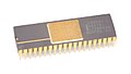
[edit]8087
[edit]The 8087 was the first math coprocessor for 16-bit processors designed by Intel. It was released in 1980 to be paired with the Intel 8088 or 8086 microprocessors. (Intel's earlier 8231 and 8232 floating-point processors, marketed for use with the i8080 CPU, were in fact licensed versions of AMD's Am9511 and Am9512 FPUs from 1977 and 1979.[6])
80C187
[edit]
Although the original 1982 datasheet for the (NMOS based) 80188 and 80186 seem to mention specific math coprocessors,[7] both chips were actually paired with an 8087.
However, in 1987, in order to work with the refreshed CMOS based Intel 80C186 CPU, Intel introduced the 80C187[8] math coprocessor. The 80C187 interface to the main processor is the same as that of the 8087, but its core is essentially that of an 80387SX and is thus fully IEEE 754-compliant and capable of executing all the 80387's extra instructions.[9]
80287
[edit]The 80287 (i287), released in 1982, is the math coprocessor for the Intel 80286 series of microprocessors. Intel's models included variants with specified upper frequency limits ranging from 6 up to 12 MHz. The NMOS version were available 6, 8 and 10 MHz.[10] The available 10 MHz Intel 80287-10 Numerics Coprocessor version was for 250 USD in quantities of 100.[11] These boxed version of 80287, 80287-8, and 80287-10 were available for USD $212, $326, and $374 respectively. There was boxed version of 80C287A available for USD $457.[12]
Other 287 models with 387-like performance are the Intel 80C287, built using CHMOS III, and the AMD 80EC287 manufactured in AMD's CMOS process, using only fully static gates.
Later followed the i80287XL with 387SX microarchitecture with a 287 pinout,[13] the i80287XLT, a special version intended for laptops, as well as other variants. It contains an internal 3/2 multiplier, so that motherboards that ran the coprocessor at 2/3 CPU speed could instead run the FPU at the same speed of the CPU. Both 80287XL and 80287XLT offered 50% better performance, 83% less power consumption, and additional instructions.[14]
The 80287 works with the 80386 microprocessor and was initially the only coprocessor available for the 80386 until the introduction of the 80387 in 1987. However, the 80387 is strongly preferred for its higher performance and more capable instruction set.
-
 6 MHz version of the Intel 80287
 -
 Intel 80287 die shot
 -
 Intel 80287XL
 -
 Intel 80287XLT


80387
[edit]
The 80387 (387 or i387) is the first Intel coprocessor to be fully compliant with the IEEE 754-1985 standard. Released in 1987,[15] two years after the 386 chip, the i387 includes much improved speed over Intel's previous 8087/80287 coprocessors and improved characteristics of its trigonometric functions. It was made available for USD $500 in quantities of 100.[16] Shortly afterwards, it was made available through Intel's Personal Computer Enhancement Operation for a retail market price of USD $795.[17] The 25 MHz version was available in retail channel for USD $1395.[18] The Intel M387 math coprocessor met under MIL-STD-883 Rev. C standard. This device was tested which includes temperature cycling between -55 and 125 °C, hermeticity sealed and extended burn-in. This military version operates at 16 MHz. This military version was available in 68-lead PGA and quad flatpack. This military version was available for USD $1155 in 100-unit of quantities for the PGA version.[19] The 33 MHz version of 387DX was available and it has the performance of 3.4 megawhetstones per second.[20] The following boxed version of 16-, 20-, 25-, and 33-MHz 387DX math coprocessor were available for USD $570, $647, $814, and $994 respectively.[21] The 8087 and 80287's FPTAN and FPATAN instructions are limited to an argument in the range ±π/4 (±45°), and the 8087 and 80287 have no direct instructions for the SIN and COS functions.[22][full citation needed]
Without a coprocessor, the 386 normally performs floating-point arithmetic through (relatively slow) software routines, implemented at runtime through a software exception handler. When a math coprocessor is paired with the 386, the coprocessor performs the floating-point arithmetic in hardware, returning results much faster than an (emulating) software library call.
The i387 is compatible only with the standard i386 chip, which has a 32-bit processor bus. The later cost-reduced i386SX, which has a narrower 16-bit data bus, can not interface with the i387's 32-bit bus. The i386SX requires its own coprocessor, the 80387SX, which is compatible with the SX's narrower 16-bit data bus. Intel released the low power version of 387SX coprocessor.[20]
In addition, to pair with the i386SL used in laptops, Intel released the i387SL (N80387SL).[23] Marketed as "Intel387 SL Mobile Math CoProcessor", it included power-management features which allowed it to run without significantly reducing battery life. There are two battery-saving power-down features. The first one stops the coprocessor's clock when the CPU goes into "stop clock" mode; the 387SL consumes about 25 microamperes when its clock is stopped. The second one operates automatically when the CPU is running, putting the 387SL into "idle mode" when it is not executing an instruction. When active, the 387SL typically consumes 30 percent less battery power (about 100 mA) than the 387SX. In idle mode, it consumes 4 mA, a 96 percent power reduction compared to the active mode. It works in the range of 16 to 25 MHz and does not require BIOS or hardware reconfiguration.[24] It was initially available for USD $189.[25]
-
 i387
i387 -
 i387SX
 -
 i387DX
 -
 i387 microarchitecture with 16-bit barrel shifter and CORDIC unit
 -
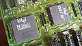 i386DX with i387DX
 -
 Socket for the 80387


80487
[edit]
Introduced in 1991, the i487SX (P23N) was marketed as a floating-point unit coprocessor for Intel i486SX machines. It actually contained a full-blown i486DX implementation. When installed into an i486SX system, the i487 disabled the main CPU and took over all CPU operations. The i487 manual claims that the unit would not function without an i486SX in place, but independent testing has revealed otherwise.[26][27]
The i487 used a special 169-pin socket with an unconnected (physical keying) pin to prevent insertion into the regular 168-pin 486 socket. One source claims that the socket is the same as Socket 1, the upgrade socket for i486 OverDrive, a processor replacement in a similar vein.[28]
The FPU instruction set of i486DX/i487SX was not different from the 387, but integration provided a bus utilisation benefit. On-chip algorithms were also improved.
Nx587
[edit]NexGen's Nx587 FPU for the Nx586 processor, released in 1995, was the last x87 coprocessor to be manufactured separately from the CPU.
See also
[edit]Notes
[edit]References
[edit]- ^ William Kahan (2 November 1990). "On the advantages of 8087's stack" (PDF). Unpublished course notes, Computer Science Division, University of California at Berkeley. Archived from the original (PDF) on 18 January 2017.
- ^ William Kahan (8 July 1989). "How Intel 8087 stack overflow/underflow should have been handled" (PDF). Archived from the original (PDF) on 12 June 2013.
- ^ Jack Woehr (1 November 1997). "A conversation with William Kahan".
- ^ David Monniaux (May 2008). "The pitfalls of verifying floating-point computations". ACM Transactions on Programming Languages and Systems. 30 (3): 1–41. arXiv:cs/0701192. doi:10.1145/1353445.1353446. S2CID 218578808.
- ^ Numbers are taken from respective processors' data sheets, programming manuals, and optimization manuals.
- ^ "Arithmetic Processors: Then and Now". www.cpushack.com. 23 September 2010. Retrieved 3 May 2023.
- ^ Intel (1983). Intel Microprocessor & Peripherals Handbook. pp. 3-25 (iAPX 186/20) and 3-106 (iAPX 188/20).
- ^ "CPU Collection – Model 80187". cpu-info.com. Archived from the original on 23 July 2011. Retrieved 14 April 2018.
- ^ "80C187 80-BIT MATH COPROCESSOR" (PDF). November 1992. Retrieved 3 May 2023.
- ^ Yoshida, Stacy, "Math Coprocessors: Keeping Your Computer Up for the Count", Intel Corporation, Microcomputer Solutions, September/October 1990, page 16
- ^ Intel Corporation, "New Product Focus Component: A 32-Bit Microprocessor With A Little Help From Some Friends", Special 32-Bit Issue Solutions, November/December 1985, page 13.
- ^ Intel Corporation, "Personal Computer Enhancement", Personal Computer Enhancement Operation, Order No. 245.2, 10-89/75K/AL/GO, October 1989, page 4
- ^ Intel Corporation, "New Product Focus: Systems: SnapIn 386 Module Upgrades PS/2 PCs", Microcomputer Solutions, September/October 1991, page 12
- ^ Yoshida, Stacy, "Math Coprocessors: Keeping Your Computer Up for the Count", Intel Corporation, Microcomputer Solutions, September/October 1990, page 16
- ^ Moran, Tom (1987-02-16). "Chips to Improve Performance Of 386 Machines, Intel Says". InfoWorld. Vol. 9, no. 7. p. 5. ISSN 0199-6649.
- ^ "New Product Focus Components: The 32-Bit Computing Engine Full Speed Ahead". Solutions. Intel Corporation: 10. May–June 1987.
- ^ "NewsBit: Intel 80387 Available Through Retail Channels". Solutions. Intel Corporation: 1. July–August 1987.
- ^ Intel Corporation, "NewsBits: 25 MHZ 80387 Available Through Retail Channels", Microcomputer Solutions, September/October 1988, page 1
- ^ Intel Corporation, "Focus: Components: Militarized Peripherals Support M386 Microprocessor", Microcomputer Solutions, March/April 1989, page 12
- ^ a b Lewnes, Ann, "The Intel386 Architecture Here to Stay", Intel Corporation, Microcomputer Solutions, July/August 1989, page 2
- ^ Intel Corporation, "Personal Computer Enhancement", Personal Computer Enhancement Operation, Order No. 245.2, 10-89/75K/AL/GO, October 1989
- ^ Borland Turbo Assembler documentation.
- ^ "Intel N80387SL". www.cpu-world.com. Retrieved 4 December 2024.
- ^ "Intel 387 SL Math Coprocessor". PC World. Vol. 10, no. 7. July 1992. p. 72.
- ^ Intel Corporation, "New Product Focus: End-User: Math Coprocessor Brings Desktop Performance To Portables", Microcomputer Solutions, May/June 1992, page 16-17
- ^ Intel 487SX at the Free On-line Dictionary of Computing
- ^ "Intel 80487". www.cpu-world.com. Retrieved 9 June 2021.
- ^ "Microprocessor Types and Specifications". InformIT. Pearson. 8 June 2001. Archived from the original on 7 December 2021.
External links
[edit]Overview
Purpose and Evolution
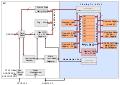
The x87 is the original floating-point unit (FPU) instruction set architecture and associated hardware for the x86 family of processors, introduced to provide dedicated support for floating-point arithmetic operations that were absent in the base integer-focused 8086 and 8088 microprocessors of the late 1970s.[3] Developed by Intel in the late 1970s and early 1980s, the x87 addressed the limitations of early x86 CPUs, which handled only integer computations and relied on software emulation for floating-point tasks, resulting in significant performance penalties for numerical applications.[4] The initial implementation, the 8087 coprocessor, was announced in 1980 alongside the 8086 to enable hardware acceleration of mathematical operations essential for scientific, engineering, and data processing workloads.[3][5] The primary motivation for x87's creation stemmed from the growing demand in personal computing for efficient floating-point arithmetic, particularly in fields like scientific simulation and engineering design, where software-based floating-point emulation on integer processors could slow computations by orders of magnitude—up to 100 times slower without dedicated hardware.[4] Intel enlisted numerical analyst William Kahan as a consultant in 1976 to design a robust floating-point system, leading to the x87's emphasis on accuracy and standardization.[6] This collaboration influenced the broader IEEE 754-1985 standard for binary floating-point arithmetic, with x87 providing implementations for single-precision (32-bit), double-precision (64-bit), and an 80-bit extended-precision format to support higher accuracy in intermediate calculations.[7][8] x87's architecture evolved from a discrete coprocessor model, where the 8087 interfaced with the main CPU via a shared bus and specialized ESCAPE instructions (opcodes D8h-DFh) to invoke floating-point operations, synchronized by the WAIT instruction (later aliased as FWAIT) to ensure completion before proceeding.[3][5] This design allowed optional integration, boosting adoption in systems like the IBM PC. By 1989, with the introduction of the 80486 microprocessor, Intel integrated the x87 FPU directly on-chip in the 80486DX variant, eliminating the need for a separate coprocessor and improving latency and efficiency for floating-point tasks.[9] Subsequent x86 generations, including the 80287 and 80387, refined this coprocessor approach before full on-die integration became standard, solidifying x87's role in x86 evolution.[3]Role in x86 Computing
The x87 floating-point unit functions as a coprocessor, originally designated the Numeric Processor eXtension (NPX), interfacing with the 8086 and 80286 processors through a shared multiplexed address-data bus and dedicated control lines for synchronization and status signaling.[10] This connection enables the x87 to access the same system memory as the integer unit, facilitating data transfer via common memory locations, while internal status and control words manage operational states such as exception masks and rounding modes.[11] Synchronization between the main CPU and x87 is achieved primarily through the FWAIT instruction, which halts the CPU until the x87 completes any pending operations and resolves unmasked exceptions, ensuring sequential execution in mixed integer-floating-point code.[12] Error conditions in the x87, such as overflows or invalid operations, are signaled via interrupt flags, with interrupt 16 (#MF) triggered for floating-point errors when the numeric error (NE) flag in control register CR0 is enabled, allowing software to handle exceptions through dedicated handlers.[13] In software, x87 integrates via assembly instructions such as FLD for loading values onto the register stack and FSTP for storing results and popping the stack, enabling direct manipulation of floating-point data in low-level code. Early high-level language support emerged with compilers like Microsoft C 5.0 in 1987, which by default generated inline instructions for 8087 or 80287 coprocessors to handle floating-point operations, with fallback to software emulation libraries like 87.LIB for systems lacking hardware.[14][15] Later x86 processors maintain backward compatibility with x87 instructions, integrating the FPU on-chip while preserving the original coprocessor interface for legacy code execution.[1] In x86-64 mode, x87 remains available despite the mandate for SSE2 support in floating-point operations, ensuring full architectural compliance for applications relying on extended-precision formats or historical binaries.[16] The x87's integration profoundly influenced the x86 ecosystem by enabling efficient floating-point computation in early DOS and Windows applications, such as scientific simulations and graphics software that previously depended on slow software emulation.[17] Operating systems like MS-DOS supported this through software floating-point emulators in compiler libraries, allowing x87-compatible code to run on hardware without a dedicated coprocessor, thus broadening accessibility for math-intensive programs.[15]Core Architecture
Register Stack and Data Handling
The x87 FPU employs eight 80-bit floating-point registers, denoted ST(0) through ST(7), arranged in a stack-based architecture that facilitates operand management for floating-point computations. The registers operate on a last-in, first-out (LIFO) principle, with ST(0) serving as the top of the stack. A 3-bit top-of-stack (TOS) pointer, located in bits 11 through 13 of the status word, dynamically indicates which register currently occupies the top position, enabling implicit addressing relative to ST(0). This design allows instructions to reference operands without explicit register numbering, promoting efficient stack manipulation while limiting direct access to eight physical registers.[1] Core stack operations include pushing and popping values to handle data flow. The FLD instruction pushes a value onto the stack by loading it into the current ST(0) and decrementing the TOS pointer, effectively shifting existing stack contents downward (e.g., the previous ST(0) becomes ST(1)). Conversely, the FSTP instruction pops the top value by storing the contents of ST(0) to memory or another location and incrementing the TOS pointer, restoring the previous top to ST(0). For scenarios requiring non-destructive access, such as swapping operands without altering the stack depth, the FXCH instruction exchanges the contents of ST(0) with another stack register, preserving the TOS position. These mechanisms ensure seamless data handling, though they can lead to stack overflow or underflow if the TOS exceeds the 0-7 range, triggering an invalid-operation exception.[1] The status word, a 16-bit register, encapsulates critical runtime information about the FPU's operational state. It includes the TOS pointer for stack tracking, condition codes C0 through C3 that reflect comparison outcomes (e.g., greater than, less than, or equal), and flags for floating-point exceptions such as invalid operation, denormal operand, zero divide, overflow, underflow, and precision. Additional bits cover the exception summary (indicating any unmasked pending exception), stack fault (signaling overflow or underflow), and busy flag (denoting ongoing FPU activity). The following table outlines the status word's bit structure:| Bit Position | Field | Description |
|---|---|---|
| 15 | B | Busy flag: 1 indicates the FPU is executing an instruction. |
| 14 | C3 | Condition code 3: Used in specific comparison and transcendental operations. |
| 13-11 | TOP | Top-of-stack pointer: 3-bit value (0-7) pointing to the current ST(0). |
| 10 | ES | Exception summary: 1 if any unmasked exception is pending. |
| 9 | SF | Stack fault: 1 if stack overflow or underflow occurred. |
| 8 | PE | Precision exception: 1 if a precision error happened. |
| 7 | UE | Underflow exception: 1 if underflow occurred. |
| 6 | OE | Overflow exception: 1 if overflow occurred. |
| 5 | ZE | Zero divide exception: 1 if division by zero attempted. |
| 4 | DE | Denormal operand exception: 1 if a denormal operand used. |
| 3 | IE | Invalid operation exception: 1 for invalid operations (e.g., NaN operands). |
| 2 | C2 | Condition code 2: Indicates equality or sign in comparisons. |
| 1 | C1 | Condition code 1: Used for parity and ordering in comparisons. |
| 0 | C0 | Condition code 0: Least significant bit for comparison results (e.g., less than). |
| Bit Position | Field | Description |
|---|---|---|
| 15-14 | Reserved | Must be 1 for compatibility. |
| 13 | PM | Precision exception mask: 1 to mask precision errors. |
| 12 | UM | Underflow exception mask: 1 to mask underflow. |
| 11 | OM | Overflow exception mask: 1 to mask overflow. |
| 10 | ZM | Zero divide exception mask: 1 to mask zero divide. |
| 9 | DM | Denormal operand exception mask: 1 to mask denormals. |
| 8 | IM | Invalid operation exception mask: 1 to mask invalid ops. |
| 7-6 | PC | Precision control: 00=single (24-bit), 10=double (53-bit), 11=extended (64-bit). |
| 5-4 | RC | Rounding control: 00=nearest, 01=toward -∞, 10=toward +∞, 11=toward 0. |
| 3-0 | Reserved | Must be 0. |
| Bits | Register | 00 (Valid) | 01 (Zero) | 10 (Special) | 11 (Empty) |
|---|---|---|---|---|---|
| 0-1 | ST(0) | Finite non-zero | +0 or -0 | NaN, ∞, denormal | No content |
| 2-3 | ST(1) | Finite non-zero | +0 or -0 | NaN, ∞, denormal | No content |
| 4-5 | ST(2) | Finite non-zero | +0 or -0 | NaN, ∞, denormal | No content |
| 6-7 | ST(3) | Finite non-zero | +0 or -0 | NaN, ∞, denormal | No content |
| 8-9 | ST(4) | Finite non-zero | +0 or -0 | NaN, ∞, denormal | No content |
| 10-11 | ST(5) | Finite non-zero | +0 or -0 | NaN, ∞, denormal | No content |
| 12-13 | ST(6) | Finite non-zero | +0 or -0 | NaN, ∞, denormal | No content |
| 14-15 | ST(7) | Finite non-zero | +0 or -0 | NaN, ∞, denormal | No content |
Supported Data Types
The x87 floating-point unit (FPU) natively supports three real number formats for high-precision arithmetic, including an Intel-specific extended precision format alongside IEEE 754 single and double precision standards. These formats enable the x87 to handle a wide range of numerical computations with varying levels of accuracy and range, primarily stored in its register stack. The extended precision serves as the default internal representation during operations, while single and double precision are used for compatibility with memory loads and stores.[1] Extended precision is an 80-bit format unique to the x87 architecture, consisting of 1 sign bit, a 15-bit exponent with a bias of 16383, and a 64-bit explicit mantissa that includes the integer bit without an implied hidden bit. This structure provides approximately 19 decimal digits of precision and an exponent range from -4931 to +4932, making it suitable for intermediate computations requiring maximal accuracy. Unlike IEEE 754 formats, the explicit leading bit in the mantissa allows for exact representation of integers up to 2^64 - 1.[1] Double precision follows the IEEE 754 standard in a 64-bit format, featuring 1 sign bit, an 11-bit exponent biased by 1023, and a 52-bit mantissa with an implied leading 1 for normalized numbers (providing about 15-16 decimal digits of precision). This format is loaded into the x87 registers using instructions like FLD and stored via FSTP, often after internal extended precision computations are rounded to match the specified precision. The exponent range spans approximately -1022 to +1023.[1] Single precision adheres to IEEE 754 in a 32-bit format, with 1 sign bit, an 8-bit exponent biased by 127, and a 23-bit mantissa including an implied leading 1 (offering around 6-7 decimal digits of precision). It is supported primarily for legacy compatibility and I/O operations, loaded and stored similarly to double precision, with an exponent range from -126 to +127.[1] In addition to real numbers, the x87 handles several integer types for conversions and scaling operations. These include 16-bit (word), 32-bit (doubleword), and 64-bit (quadword) signed or unsigned integers, which can be loaded via FILD and stored with FIST or FISTP. A specialized 80-bit packed binary-coded decimal (BCD) format encodes up to 18 decimal digits (72 bits) plus a sign bit in the tenth byte, enabling precise decimal arithmetic without floating-point conversion errors. Temporary integers are also generated internally during operations like scaling or rounding, but they are not directly storable as persistent data types.[1] The x87 fully supports IEEE 754 special values across its formats, including Not-a-Number (NaN), infinity, and denormalized numbers. NaNs are encoded with an all-1s exponent and non-zero mantissa, distinguishing quiet NaNs (which propagate without exceptions) from signaling NaNs (which raise invalid operation exceptions). Infinities result from exponent all 1s with zero mantissa, indicating ±∞ from overflows or division by zero. Denormals use an all-0s exponent with non-zero mantissa, lacking the implied leading 1 to represent subnormal values near zero. Gradual underflow is managed through denormals, gradually reducing precision as values approach zero, while exponent overflow triggers infinity or the maximum finite value, potentially raising a numeric overflow exception depending on the control word masking.[1]| Format | Bits | Sign | Exponent (Bias) | Mantissa | Precision (Decimal Digits) | Exponent Range |
|---|---|---|---|---|---|---|
| Extended | 80 | 1 | 15 (16383) | 64 (explicit) | ~19 | -4931 to +4932 |
| Double | 64 | 1 | 11 (1023) | 52 (implied 1) | ~15-16 | -1022 to +1023 |
| Single | 32 | 1 | 8 (127) | 23 (implied 1) | ~6-7 | -126 to +127 |