
Community hub
Recent from talks
Contribute something
Nothing was collected or created yet.
Intel 80286
View on Wikipedia
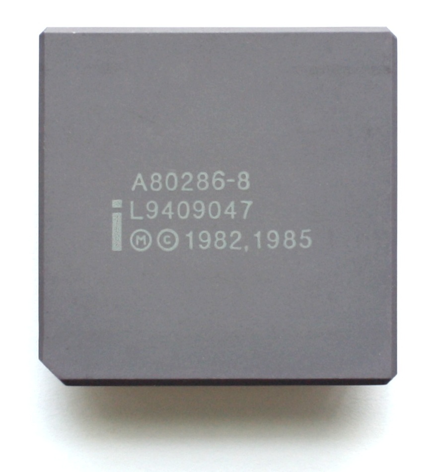
 An Intel A80286-8 processor with a gray ceramic heat spreader | |
| General information | |
|---|---|
| Launched | February 1982 |
| Discontinued | 1991[1] |
| Common manufacturer | |
| Performance | |
| Max. CPU clock rate | 4 MHz to 25 MHz |
| FSB speeds | 4 MHz to 25 MHz |
| Data width | 16 bits |
| Address width | 24 bits |
| Architecture and classification | |
| Technology node | 1.5 μm[2] |
| Instruction set | x86-16 (with MMU) |
| Physical specifications | |
| Transistors | |
| Co-processor | Intel 80287 |
| Packages | |
| Sockets |
|
| History | |
| Predecessors | 8086, 8088 (while 80186 was contemporary) |
| Successor | Intel 80386 |
| Support status | |
| Unsupported | |
The Intel 80286[4] (also marketed as the iAPX 286[5] and often called Intel 286) is a 16-bit microprocessor that was introduced on February 1, 1982. It was the first 8086-based CPU with separate, non-multiplexed address and data buses and also the first with memory management and wide protection abilities. It had a data size of 16 bits, and had an address width of 24 bits, which could address up to 16MB of memory with a suitable operating system such as Windows compared to 1MB for the 8086. The 80286 used approximately 134,000 transistors in its original nMOS (HMOS) incarnation and, just like the contemporary 80186,[6] it can correctly execute most software written for the earlier Intel 8086 and 8088 processors.[7]
The 80286 was employed for the IBM PC/AT, introduced in 1984, and then widely used in most PC/AT compatible computers until the early 1990s. In 1987, Intel shipped its five-millionth 80286 microprocessor.[8]
History and performance
[edit]
Intel's first 80286 chips were specified for a maximum clockrate of 5, 6 or 8 MHz and later releases for 12.5 MHz. AMD and Harris later produced 16 MHz, 20 MHz and 25 MHz parts. Intel, Intersil and Fujitsu also designed fully static CMOS versions of Intel's original depletion-load nMOS implementation, largely aimed at battery-powered devices. Intel's CMOS version of the 80286 was the 80C286.
On average, the 80286 was said to have a speed of about 0.21 instructions per clock on "typical" programs,[9] although it could be significantly faster on optimized code and in tight loops, as many instructions could execute in 2 clock cycles each. The 6 MHz, 10 MHz, and 12 MHz models were reportedly measured to operate at 0.9 MIPS, 1.5 MIPS, and 2.66 MIPS respectively.[10]
The later E-stepping level of the 80286 was free of the several significant errata that caused problems for programmers and operating-system writers in the earlier B-step and C-step CPUs (common in the AT and AT clones). This E-2 stepping part may have been available in later 1986.[11]
Intel second sourced this microprocessor to Fujitsu Limited in about 1985.[12]
Variants
[edit]| Model number | Frequency | Technology | Process | Package | Date of release | Price USD[list 1] |
|---|---|---|---|---|---|---|
| 80286-10[13] | 10 MHz | HMOS-III | 1.5 μm | July/August 1985 | $155 | |
| 80286-12[13] | 12.5 MHz | HMOS-III | 1.5 μm | July/August 1985 | $260 | |
| MG80286[14] | September/October 1985 | $784 | ||||
| 80286[15] | 68 Pin PGA[list 2] | January/February 1986 | ||||
| 80286[15] | 68 Pin PLCC[list 3] | January/February 1986 |
Architecture
[edit]

Intel expected the 286 to be used primarily in industrial automation, transaction processing, and telecommunications, instead of in personal computers.[16]
The CPU was designed for multi-user systems with multitasking applications, including communications (such as automated PBXs) and real-time process control. It had 134,000 transistors and consisted of four independent units: the address unit, bus unit, instruction unit, and execution unit, organized into a loosely coupled (buffered) pipeline, just as in the 8086. It was produced in a 68-pin package, including PLCC (plastic leaded chip carrier), LCC (leadless chip carrier) and PGA (pin grid array) packages.[17]
The performance increase of the 80286 over the 8086 (or 8088) could be more than 100% per clock cycle in many programs (i.e., a doubled performance at the same clock speed). This was a large increase, fully comparable to the speed improvements seven years later when the i486 (1989) or the original Pentium (1993) were introduced. This was partly due to the non-multiplexed address and data buses, but mainly to the fact that address calculations (such as base+index) were less expensive. They were performed by a dedicated unit in the 80286, while the older 8086 had to do effective address computation using its general ALU, consuming several extra clock cycles in many cases. Also, the 80286 was more efficient in the prefetch of instructions, buffering, execution of jumps, and in complex microcoded numerical operations such as MUL/DIV than its predecessor.[18]
The 80286 included, in addition to all of the 8086 instructions, all of the new instructions of the 80186: ENTER, LEAVE, BOUND, INS, OUTS, PUSHA, POPA, PUSH immediate, IMUL immediate, and immediate shifts and rotates. The 80286 also added new instructions for protected mode: ARPL, CLTS, LAR, LGDT, LIDT, LLDT, LMSW, LSL, LTR, SGDT, SIDT, SLDT, SMSW, STR, VERR, and VERW. Some of the instructions for protected mode can (or must) be used in real mode to set up and switch to protected mode, and a few (such as SMSW and LMSW) are useful for real mode itself.
The Intel 80286 had a 24-bit address bus and as such had a 16 MB physical address space, compared to the 1 MB address space of prior x86 processors. It was the first x86 processor to support virtual memory supporting up to 1 GB via segmentation.[19] However, memory cost and the initial rarity of software using the memory above 1 MB meant that until late in its production, 80286 computers rarely shipped with more than 1 MB of RAM.[18] Additionally, there was a performance penalty involved in accessing extended memory from real mode as noted below.
Features
[edit]


Protected mode
[edit]The 286 was the first of the x86 CPU family to support protected virtual-address mode, commonly called "protected mode". In addition, it was the first commercially available microprocessor with on-chip memory management unit (MMU) capabilities (systems using the contemporaneous Motorola 68010 and NS320xx could be equipped with an optional MMU controller). This would allow IBM compatibles to have advanced multitasking OSes for the first time and compete in the Unix-dominated[20] server/workstation market.
Several additional instructions were introduced in the protected mode of 80286, which are helpful for multitasking operating systems.
Another important feature of 80286 is the prevention of unauthorized access. This is achieved by:
- Forming different segments for data, code, and stack, and preventing their overlapping.
- Assigning privilege levels to each segment. Segments with lower privilege levels cannot access segments with higher privilege levels.
In 80286 (and in its co-processor Intel 80287), arithmetic operations can be performed on the following different types of numbers:
- unsigned packed decimal,
- unsigned binary,
- unsigned unpacked decimal,
- signed binary,
- floating-point numbers (only with an 80287).
By design, the 286 could not revert from protected mode to the basic 8086-compatible real address mode ("real mode") without a hardware-initiated reset. In the PC/AT introduced in 1984, IBM added external circuitry, as well as specialized code in the ROM BIOS and the 8042 keyboard microcontroller to enable software to cause the reset, allowing real-mode reentry while retaining active memory and returning control to the program that initiated the reset. (The BIOS is necessarily involved because it obtains control directly whenever the CPU resets.) Though it worked correctly, the method imposed a huge performance penalty.
In theory, real-mode applications could be directly executed in 16-bit protected mode if certain rules (newly proposed with the introduction of the 80286) were followed; however, as many DOS programs did not conform to those rules, protected mode was not widely used until the appearance of its successor, the 32-bit Intel 80386, which was designed to go back and forth between modes easily and to provide an emulation of real mode within protected mode. When Intel designed the 286, it was not designed to be able to multitask real-mode applications; real mode was intended to be a simple way for a bootstrap loader to prepare the system and then switch to protected mode; essentially, in protected mode the 80286 was designed to be a new processor with many similarities to its predecessors, while real mode on the 80286 was offered for smaller-scale systems that could benefit from a more advanced version of the 80186 CPU core, with advantages such as higher clock rates, faster instruction execution (measured in clock cycles), and unmultiplexed buses, but not the 24-bit (16 MB) memory space.
To support protected mode, new instructions have been added: ARPL, VERR, VERW, LAR, LSL, SMSW, SGDT, SIDT, SLDT, STR, LMSW, LGDT, LIDT, LLDT, LTR, CLTS. There are also new exceptions (internal interrupts): invalid opcode, coprocessor not available, double fault, coprocessor segment overrun, stack fault, segment overrun/general protection fault, and others only for protected mode.
OS support
[edit]The protected mode of the 80286 was not routinely utilized in PC applications until many years after its release, in part because of the high cost of adding extended memory to a PC, but also because of the need for software to support the large user base of 8086 PCs. For example, in 1986 the only program that made use of it was VDISK, a RAM disk driver included with PC DOS 3.0 and 3.1. A DOS could utilize the additional RAM available in protected mode (extended memory) either via a BIOS call (INT 15h, AH=87h), as a RAM disk, or as emulation of expanded memory.[18]
The difficulty lay in the incompatibility of older real-mode DOS programs with protected mode. They could not natively run in this new mode without significant modification. In protected mode, memory management and interrupt handling were done differently than in real mode. In addition, DOS programs typically would directly access data and code segments that did not belong to them, as real mode allowed them to do without restriction; in contrast, the design intent of protected mode was to prevent programs from accessing any segments other than their own unless special access was explicitly allowed. While it was possible to set up a protected-mode environment that allowed all programs access to all segments (by putting all segment descriptors into the Global Descriptor Table (GDT) and assigning them all the same privilege level), this undermined nearly all of the advantages of protected mode except the extended (24-bit) address space. The choice that OS developers faced was either to start from scratch and create an OS that would not run the vast majority of the old programs, or to come up with a version of DOS that was slow and ugly (i.e., ugly from an internal technical viewpoint) but would still run a majority of the old programs. Protected mode also did not provide a significant enough performance advantage over the 8086-compatible real mode to justify supporting its capabilities; actually, except for task switches when multitasking, it yielded a performance disadvantage, by slowing down many instructions through a litany of added privilege checks. In protected mode, registers were still 16-bit, and the programmer was still forced to use a memory map composed of 64 kB segments, just like in real mode.[21]
Intel had not expected the lack of virtual machine support for 8086 software to be a problem, because it thought that new software using all of the 80286's capabilities would quickly appear. Bill Gates referred to the 80286 as a "brain-damaged" chip, because it cannot use virtual machines to multitask multiple MS-DOS applications[22] with an operating system like Microsoft Windows. It was arguably responsible for the split between Microsoft and IBM, since IBM insisted that OS/2, originally a joint venture between IBM and Microsoft, would run on a 286 (and in text mode). [22]
In January 1985, Digital Research previewed the Concurrent DOS 286 1.0 operating system developed in cooperation with Intel. The product would function strictly as an 80286 native-mode (i.e. protected-mode) operating system, allowing users to take full advantage of the protected mode to perform multi-user, multitasking operations while running 8086 emulation.[23][24][25] This worked on the B-1 prototype step of the chip, but Digital Research discovered problems with the emulation on the production level C-1 step in May, which would not allow Concurrent DOS 286 to run 8086 software in protected mode. The release of Concurrent DOS 286 was delayed until Intel would develop a new version of the chip.[23] In August, after extensive testing on E-1 step samples of the 80286, Digital Research acknowledged that Intel corrected all documented 286 errata, but said that there were still undocumented chip performance problems with the prerelease version of Concurrent DOS 286 running on the E-1 step. Intel said that the approach Digital Research wished to take in emulating 8086 software in protected mode differed from the original specifications. Nevertheless, in the E-2 step, they implemented minor changes in the microcode that would allow Digital Research to run emulation mode much faster.[11] Named IBM 4680 OS, IBM originally chose DR Concurrent DOS 286 as the basis of their IBM 4680 computer for IBM Plant System products and point-of-sale terminals in 1986.[26] Digital Research's FlexOS 286 version 1.3, a derivation of Concurrent DOS 286, was developed in 1986, introduced in January 1987, and later adopted by IBM for their IBM 4690 OS, but the same limitations affected it.
Other operating systems that used the protected mode of the 286 were Microsoft Xenix (around 1984),[27] Coherent,[28] and Minix.[29] These were less hindered by the limitations of the 80286 protected mode because they did not aim to run MS-DOS applications or other real-mode programs.
When designing the 80386 Intel engineers were aware of, and agreed with, the 80286's poor reputation.[30] They enhanced the 80386's protected mode to address more memory, and also added the separate virtual 8086 mode, a mode within protected mode with much better MS-DOS compatibility.[31]
Support components
[edit]
This is a list of bus interface components that connect to an Intel 80286 microprocessor.
- 82230/82231 High Integration AT-Compatible Chip Set – The 82230 covers this combination of chips: 82C284 clock, 82288 bus controller, and dual 8259A interrupt controllers among other components. The 82231 covers this combination of chips: 8254 interrupt timer, 74LS612 memory mapper and dual 8237A DMA controller among other components. They were available by second-sourced with Zymos Corp. Both set are available USD $60 for 10 MHz version and USD $90 for 12 MHz version in quantities of 100.[32]
- 82258 Advanced Direct Memory Access Controller – Transfer rate of 8MB per second, supports up to 32 subchannels, mask and compare, verify, translation, and assembly/disassembly operation that are being processed simultaneously. It also supports a 16MB addressing range. These were available for USD $170 in quantities of 100.[33]
- 82284[34] and 82C284[35] Clock Generator and Driver – Intel second sourced this 82284 version to Fujitsu Limited around 1985.[36] The Intel branded chipset was available in 20-pin PLCC in sampling at first quarter 1986.[15]
- 82288 Bus Controller, a bus controller supplied in 20-pin DIP package. It replaces 8288 used with earlier processors. Intel second sourced this chipset to Fujitsu Limited around 1985.[37] The 20-pin PLCC version was available in sampling for first quarter of 1986.[38]
- 82289 Arbiter
See also
[edit]- U80601 – Almost identical copy of the 80286 manufactured 1989/1990 in East Germany. In the Soviet Union a clone of the 80286 was designated KR1847VM286 (Russian: КР1847ВМ286).[39]
- iAPX, for the iAPX name
- LOADALL – Undocumented 80286/80386 instruction that could be used to gain access to all available memory in real mode.
- Windows/286
References
[edit]- ^ "CPU History - The CPU Museum - Life Cycle of the CPU". cpushack.com. Archived from the original on July 20, 2021. Retrieved September 6, 2021.
- ^ "1.5 μm lithography process - WikiChip". en.wikichip.org. Archived from the original on September 9, 2018. Retrieved January 21, 2019.
- ^ Ormsby, John, "Chip Design: A Race Worth Winning", Intel Corporation, Microcomputer Solutions, July/August 1988, page 18
- ^ "Microprocessor Hall of Fame". Intel. Archived from the original on July 6, 2007. Retrieved August 11, 2007.
- ^ iAPX 286 Programmer's Reference (PDF). Intel. 1983. page 1-1. Archived (PDF) from the original on August 28, 2017. Retrieved August 28, 2017.
- ^ A simpler cousin in the 8086-line with integrated peripherals, intended for embedded systems.
- ^ "Intel Museum – Microprocessor Hall of Fame". Intel.com. May 14, 2009. Archived from the original on March 12, 2009. Retrieved June 20, 2009.
- ^ Teixeira, Kevin, "What's Next For The 80286?", Intel Corporation, Microcomputer Solutions, November/December 1987, page 16
- ^ "Intel Architecure [sic] Programming and Information". Intel80386.com. January 13, 2004. Retrieved April 28, 2009.
- ^ "80286 Microprocessor Package, 1982". Content.cdlib.org. Archived from the original on March 6, 2019. Retrieved April 28, 2009.
- ^ a b Foster, Edward (August 26, 1985). "Intel shows new 80286 chip – Future of DRI's Concurrent DOS 286 still unclear after processor fixed". InfoWorld. Vol. 7, no. 34. InfoWorld Media Group. p. 21. ISSN 0199-6649. Archived from the original on January 25, 2014. Retrieved December 25, 2021.
- ^ Intel Corporation, "NewsBits: Second Source News", Solutions, January/February 1985, Page 1.
- ^ a b Intel Corporation, "New Product Focus Components: 80286 Workhorses: Twice As Fast", Solutions, July/August 1985, Page 17.
- ^ Intel Corporation, "New Product Focus Components: Highest Ranking 16-bit Microprocessor Meets Military Objectives", Solutions, September/October 1985, page 13.
- ^ a b c Ashborn, Jim; "Advanced Packaging: A Little Goes A Long Way", Intel Corporation, Solutions, January/February 1986, Page 2
- ^ Gross, Neil; Coy, Peter (March 6, 1995). "The Technology Paradox". Bloomberg. Retrieved March 19, 2020.
- ^ "Intel 80286 microprocessor family". CPU-World. Archived from the original on March 31, 2012. Retrieved May 19, 2012.
- ^ a b c Bahadure, Nilesh B. (2010). "15 Other 16-bit microprocessors 80186 and 80286". Microprocessors: 8086/8088, 80186/80286, 80386/80486 and the Pentium Family. PHI Learning Pvt. Ltd. pp. 503–537. ISBN 978-8120339422. Archived from the original on February 27, 2017. Retrieved October 11, 2016.
- ^ Intel Corporation, "New Product Focus Components: Highest Ranking 16-bit Microprocessor Meets Military Objectives", Solutions, September/October 1985, page 13
- ^ "DOS Days - IBM OS/2". dosdays.co.uk. Retrieved May 19, 2025.
- ^ Petzold, Charles (1986). "Obstacles to a grown up operating system". PC Magazine. 5 (11): 170–74. Archived from the original on February 27, 2017. Retrieved October 11, 2016.
- ^ a b Dewar, Robert B. K.; Smosna, Matthew (1990). Microprocessors: A Programmer's View. New York: McGraw-Hill. p. 110. ISBN 0-07-016638-2.
- ^ a b Foster, Edward (May 13, 1985). "Super DOS awaits new 80286 – Concurrent DOS 286 – delayed until Intel upgrades chip – offers Xenix's power and IBM PC compatibility". InfoWorld. Vol. 7, no. 19. InfoWorld Media Group. pp. 17–18. ISSN 0199-6649. Archived from the original on February 27, 2017. Retrieved October 11, 2016.
- ^ FlexOS Supplement for Intel iAPX 286-based Computers (PDF). 1.3 (1 ed.). Digital Research, Inc. November 1986. Archived (PDF) from the original on April 21, 2019. Retrieved August 14, 2018.
- ^ "Concurrent DOS 68K 1.2 - Developer Kit for Motorola VME/10 - Disk 2". August 6, 1986 [1986-04-08]. Archived from the original on April 3, 2019. Retrieved September 13, 2018. (NB. This package also includes some header files from Concurrent DOS 286, including STRUCT.H explicitly mentioning LOADALL for "8086 emulation".)
- ^ Calvo, Melissa; Forbes, Jim (February 10, 1986). "IBM to use a DRI operating system". InfoWorld. Vol. 8, no. 8. p. 12. Archived from the original on April 21, 2019. Retrieved September 6, 2011.
- ^ "Microsoft XENIX 3.0 Ready for 286" (PDF). Archived from the original (PDF) on January 7, 2014.
- ^ "An Introduction to Coherent: General Information FAQ for the Coherent Operating System". Archived from the original on June 4, 2016. Retrieved January 7, 2014.
- ^ "MINIX INFORMATION SHEET". Archived from the original on January 7, 2014.
- ^ Crawford, John; Hill, Gene; Leukhardt, Jill; Prak, Jan Willem; Slager, Jim. "Intel 386 Microprocessor Design and Development Oral History Panel" (PDF) (Interview). Interviewed by Jim Jarrett. Mountain View, California: Computer History Museum. Retrieved May 15, 2025.
- ^ Petzold, Charles (November 25, 1986). "Intel's 32-bit Wonder: The 80386 Microprocessor". PC Magazine. pp. 150–152.
- ^ Ormsby, John, Editor, "New Product Focus: Components: Intel's 82X3X Chip-set Handles Logic Functions That Once Required The Services Of Sources Of Chips", Intel Corporation, Microcomputer Solutions, January/February 1988, page 13
- ^ Intel Corporation, "New Product Focus Components: The 82258 ADMA Boost iAPX 286 Family Performance", Solutions, November/December 1984, Page 14.
- ^ iAPX 286 Hardware Reference Manual (PDF). Intel. 1983.
- ^ 80286 Hardware Reference Manual (PDF). Intel. 1987.
- ^ Intel Corporation, "NewsBits: Second Source News", Solutions, January/February 1985, Page 1
- ^ Intel Corporation, "NewsBits: Second Source News", Solutions, January/February 1985, Page 1
- ^ Ashborn, Jim; "Advanced Packaging: A Little Goes A Long Way", Intel Corporation, Solutions, January/February 1986, Page 2
- ^ "Soviet microprocessors, microcontrollers, FPU chips and their western analogs". CPU-world. Archived from the original on February 9, 2017. Retrieved March 24, 2016.
External links
[edit]- Intel Datasheets
- Intel 80286 and 80287 Programmer's Reference Manual at bitsavers.org
- Intel 80286 Programmer's Reference Manual 1987 (txt). Hint: use e.g. Hebrew (IBM-862) encoding.
- Linux on 286 laptops and notebooks
- Intel 80286 images and descriptions at cpu-collection.de
- CPU-INFO: 80286, in-depth processor history
- Overview of all 286 compatible chips
- Intel 80286 CPU Information, including chip errata and undocumented behaviour
- Intel 80286 Hardware Reference Manual
Intel 80286
View on GrokipediaDevelopment and history
Design origins
Development of the Intel 80286, initially known as the iAPX 286, began in 1978 as a successor to the 8086 microprocessor, with the primary aim of extending the 16-bit architecture to support larger memory spaces through a 24-bit address bus capable of addressing up to 16 MB of physical memory.[4][5] This extension was driven by the need to overcome the 8086's limitations, particularly its 20-bit addressing that restricted physical memory to 1 MB and lacked built-in protection mechanisms, which often led to system instability and crashes in multi-tasking environments.[6] Key design goals included the introduction of a protected mode to enhance operating system stability by providing memory protection, enabling support for multitasking and virtual memory addressing up to 1 GB per task, all while ensuring full backward compatibility with existing 8086 software through a real mode that emulated the predecessor's behavior.[6] The architecture retained the 16-bit data bus from the 8086 and 8088 for continuity but incorporated advanced segmentation in both real and protected modes, along with paging in protected mode, to facilitate more sophisticated memory handling for emerging multi-user and real-time applications.[6][5] The 80286 was fabricated with approximately 134,000 transistors using Intel's HMOS II process technology, which provided the density and performance needed for these enhancements, and later versions transitioned to CMOS implementations to reduce power consumption.[5]Release and adoption
The Intel 80286 microprocessor was announced by Intel on February 1, 1982, marking a significant advancement in 16-bit computing architecture.[7] Initial production models operated at clock speeds of 5 MHz, 6 MHz, or 8 MHz, targeting applications in high-performance personal computers and embedded systems.[8] These early variants were fabricated using HMOS technology, with the processor featuring 134,000 transistors and supporting up to 16 MB of memory in protected mode.[9] Adoption accelerated following the release of the IBM Personal Computer AT (PC/AT) in August 1984, which utilized the 80286 as its core processor running at 6 MHz.[10] This integration established the 80286 as the de facto standard for mid-1980s personal computers, enabling enhanced multitasking and memory management capabilities that propelled the evolution of PC hardware.[11] By 1987, Intel had shipped approximately 5 million units of the 80286, reflecting robust demand driven by the proliferation of AT-compatible systems from manufacturers like Compaq and IBM.[12] The processor's protected mode facilitated the development of advanced operating systems, including Microsoft Windows/286 (part of Windows 2.0 in 1987) and IBM's OS/2 1.0 (released in 1987), which leveraged its virtual memory and segmentation features for improved stability and resource allocation.[13] Early production encountered reliability issues with the A-stepping version released in 1982, which included bugs affecting interrupt handling and mode switching that could lead to system instability.[14] These were addressed in the B-stepping revision introduced in 1983, which fixed several errata related to bus timing and error inputs, enhancing compatibility for broader deployment.[14] Further refinements came with the E-stepping in 1986, providing a more stable implementation free of prior significant flaws, particularly beneficial for operating system developers.[15] Production evolved with the introduction of CMOS-based variants, such as the 80C286, starting around 1984 to support low-power applications in portable computers and embedded systems.[11] These variants offered reduced power consumption compared to the original NMOS designs, facilitating their use in battery-powered laptops and industrial controllers. The 80286 line was ultimately discontinued by Intel in 1991, as the superior Intel 80386 captured market dominance with its 32-bit capabilities.[16]Technical specifications
Performance metrics
The Intel 80286 microprocessor was produced in clock speeds ranging from 4 MHz to 25 MHz, though typical deployments in systems like the IBM PC/AT operated at 6–12 MHz to balance performance and compatibility with contemporary hardware.[17] Higher-speed variants, such as 20–25 MHz models from second-sourced manufacturers like AMD, were used in specialized or later applications but required enhanced cooling and support circuitry.[18] Performance was enhanced by limited internal pipelining, yielding an average of 0.21–0.35 instructions per clock (IPC) on typical workloads, which translated to up to 2.66 million instructions per second (MIPS) at 12 MHz.[9] In real mode, the 80286 delivered 3–6 times the throughput of the 8086 at equivalent or lower clock speeds, primarily due to faster instruction execution and a larger prefetch queue.[19] The 16-bit external data bus supported peak transfer rates of 8 MB/s for word-sized operations with zero wait states at 8 MHz, though effective bandwidth in real-mode systems averaged lower due to bus arbitration and memory timings.[2] Power consumption depended on the fabrication process and speed grade: HMOS implementations drew 2–3 W at 10 MHz, while low-power CMOS variants (e.g., 80C286) consumed approximately 0.4 W under similar conditions.[17] In protected mode, early multitasking environments incurred 20–30% efficiency overhead from segment management and context switching, limiting overall gains compared to real-mode operation. Benchmark results, such as Dhrystone, ranged from 0.8 DMIPS at 6 MHz to 1.2 DMIPS at higher steppings like the E revision, which improved prefetch efficiency for branched code paths.[20]Physical and electrical characteristics
The Intel 80286 was fabricated using a 1.5 µm HMOS II process technology, resulting in a die size of 47 mm² containing approximately 134,000 transistors.[21] Later variants, such as the low-power CMOS implementations, maintained similar dimensions while improving efficiency through CHMOS fabrication.[2] The processor was housed in 68-pin packages, either in a JEDEC-approved plastic leaded chip carrier (PLCC) or pin grid array (PGA) form factor, providing the necessary connections for address, data, control, and power signals.[2] Electrically, it required a single +5 V DC power supply delivered through dedicated Vcc pins, with ground referenced to 0 V, and featured TTL-compatible input/output levels for compatibility with contemporary logic families; clock inputs operated between 0.6 V low and 3.8 V high.[2] Thermal design power reached up to 3 W at higher clock speeds (such as 10–12 MHz), necessitating passive heatsinks or airflow in densely packed or high-end systems to maintain junction temperatures below 70°C.[17] Manufacturing was led by Intel, with second-sourcing agreements enabling production by licensees including IBM to meet demand for systems like the IBM PC/AT, resulting in widespread availability through the late 1980s.[22]Processor architecture
Internal organization
The Intel 80286 microprocessor is organized into four primary functional units that operate in a loosely coupled pipeline to handle instruction processing and data flow: the Bus Interface Unit (BIU), Instruction Unit (IU), Execution Unit (EU), and Address Unit (AU). The BIU manages external bus interfaces, including fetching instructions and data from memory or I/O devices, while generating the necessary address, data, and control signals; it also maintains the prefetch queue and overlaps bus cycles to improve efficiency. The IU receives prefetched instructions from the BIU, decodes them, and places decoded operations into a queue for the EU. The EU performs the actual arithmetic, logical, and control operations specified by decoded instructions, requesting data transfers through the BIU as needed. The AU calculates physical addresses by translating logical addresses using segment registers and offsets, supporting the overall memory access requirements of the processor.[23][24] These units enable a four-stage pipelined architecture, consisting of instruction prefetch (handled by the BIU), decode (by the IU), execution (by the EU), and address translation (by the AU), allowing overlapping of operations to enhance throughput without full superscalar capabilities. Complex instructions are implemented using microcode stored internally, which breaks them down into simpler sequences executed by the EU, while simpler instructions proceed directly through hardware paths. This pipelining reduces idle time on the bus and internal paths, though stalls can occur on branches or data dependencies that flush the pipeline.[23][25] The 80286 includes a set of 16-bit registers for general-purpose operations, such as the accumulator (AX), base (BX), counter (CX), data (DX), source index (SI), destination index (DI), base pointer (BP), and stack pointer (SP), which the EU uses for data manipulation and addressing. Segment registers—code segment (CS), data segment (DS), stack segment (SS), and extra segment (ES)—are also 16-bit and provide base addresses for segmented memory access, managed primarily by the AU. The BIU computes and maintains a 24-bit physical address for instruction prefetch by combining the 16-bit instruction pointer (IP) offset with the CS segment base, enabling access to up to 16 MB in protected mode.[25][23] To minimize bus wait states, the BIU employs a 6-byte prefetch queue that buffers upcoming instructions during idle cycles, assuming sequential execution until a branch or interrupt alters the flow. This queue feeds directly into the IU for decoding, allowing the BIU to continue prefetching while the EU processes prior instructions, thereby sustaining pipeline flow. The prefetch mechanism activates when the queue has at least two bytes free and aligns fetches on even byte boundaries for efficiency.[23][24] The internal logic of the 80286 operates at the processor clock frequency (1x), derived from the system clock input via a generator like the 82C284, which may divide higher crystal frequencies by two to produce rates such as 6, 8, 10, or 12.5 MHz. Unlike later processors with clock multipliers for higher internal speeds, the 80286's design ties execution directly to this clock without acceleration, ensuring synchronous operation across units but limiting peak performance to bus cycle timings of about 250 ns at 8 MHz.[23][25]Instruction set
The Intel 80286 instruction set maintains full backward compatibility with the 8086 in real address mode, enabling unmodified execution of 8086 software while delivering 4-6 times the performance due to internal architectural improvements.[3] It encompasses over 100 instructions from the 8086 base, categorized into data transfer, arithmetic, logical, string manipulation, control transfer, and high-level operations, with a total of approximately 160 instructions when including coprocessor extensions.[3] Representative arithmetic instructions include ADD (addition), MUL (unsigned multiplication), and their signed variants like IMUL; logical operations feature AND (bitwise AND), XOR (exclusive OR), and TEST (logical comparison); control instructions cover JMP (unconditional jump), INT (software interrupt), and IRET (interrupt return).[3] The 80286 introduces several new instructions to support enhanced memory management and programming constructs. LES loads a 32-bit pointer into a general-purpose register and the ES segment register, while LSS performs a similar operation for the SS segment register, facilitating efficient segment descriptor access.[3] BOUND verifies that a register value falls within specified array bounds, generating interrupt 5 if the condition fails, which aids in runtime error detection for array operations.[3] Addressing modes in the 80286 build on the 8086 foundation, supporting register (e.g., direct access to AX or BX), immediate (embedded constants), direct (fixed memory displacement), indirect (via base registers like BP), and indexed (combinations such as [BX + SI + displacement]) modes.[3] All memory references employ a segment:offset format, where a 16-bit segment selector pairs with a 16-bit offset to form a 20-bit linear address in real mode or a selector-based reference in protected mode.[3] Interrupt handling expands to a 256-entry vector table, allowing vectored interrupts for both software (via INT) and hardware sources.[3] External maskable interrupts are signaled through the INTR pin, which prompts the processor to fetch the interrupt vector from the bus.[3] Stack-related extensions include PUSHA, which pushes all general-purpose registers onto the stack in a fixed order (AX, CX, DX, BX, SP original value, BP, SI, DI), and POPA, which reverses this process, streamlining bulk register save/restore operations.[3] These instructions operate exclusively on 16-bit words, as the 80286 lacks native 32-bit register support, a limitation addressed in subsequent processors like the 80386.[3]Memory management
Real mode operation
The Intel 80286 initializes in Real-Address Mode, also known as Real Mode, upon power-on or reset, providing backward compatibility with earlier x86 processors such as the 8086 and 8088.[3] In this mode, the processor emulates the 8086 architecture exactly, allowing existing 8086 software, including MS-DOS applications, to execute without modification while achieving 4 to 6 times faster performance due to internal enhancements like pipelining and a faster clock rate.[3] At power-on, the code segment register (CS) is set to F000H and the instruction pointer (IP) to FFF0H, resulting in the first instruction fetch from physical address FFFFF0H, with data, extra, and stack segment registers (DS, ES, SS) initialized to 0000H.[3] Real Mode employs a 20-bit physical addressing scheme, restricting the total addressable memory to 1 MB (from 00000H to FFFFFH).[3] Physical addresses are calculated by shifting the 16-bit value in a segment register left by 4 bits (effectively multiplying by 16) to form the segment base address, then adding a 16-bit offset, yielding the final 20-bit address as segment_base + offset.[3] The four segment registers—CS for code, DS for data, SS for stack, and ES for extra data—each define a maximum 64 KB segment, with segments aligned to 16-byte boundaries and capable of overlapping to facilitate efficient memory usage in programs.[3] There is no hardware-enforced memory protection in Real Mode; all memory access is direct and unrestricted, permitting programs to read or write any location within the 1 MB space without safeguards against overruns or conflicts.[3] Memory operations in Real Mode support a flat addressing model optionally, achieved by setting segment registers to zero-based values for contiguous access across the full 1 MB space, though the segmented structure remains inherent.[3] Bus cycles for read and write operations utilize 16-bit data transfers, with aligned word accesses completing in one cycle and unaligned accesses requiring two cycles; wait states may be inserted depending on external memory timing requirements.[3] Unlike Protected Mode, Real Mode lacks paging or virtual memory translation, relying solely on the physical address bus for direct hardware access.[3] Key limitations include the 1 MB address ceiling, potential for segment wraparound (e.g., segment FFFFH:000FH equates to 0010H:000FH), and exception handling differences such as interrupt 13H for segment overrun errors, which were not present in the 8086.[3]Protected mode operation
The Intel 80286's protected mode, also known as protected virtual-address mode, expands the processor's addressing capabilities beyond the 1 MB limit of real mode by employing 24-bit physical addresses, thereby supporting up to 16 MB of physical memory.[3] This mode utilizes a segmented memory architecture where segments are defined through descriptors stored in descriptor tables, specifically the Global Descriptor Table (GDT) for system-wide segments and the Local Descriptor Table (LDT) for task-specific segments.[3] Each descriptor is an 8-byte structure containing the segment's base address, limit, and access attributes, enabling the operating system to enforce memory boundaries and protection.[3] While protected mode maintains compatibility with real mode instructions, it introduces hardware-enforced isolation to support multitasking and secure execution.[3] Entry into protected mode requires a two-step initialization process starting from real mode. First, the LGDT instruction loads the GDT register with the base address and limit of the GDT, establishing the foundation for segment addressing.[3] Subsequently, the LMSW instruction sets the Protection Enable (PE) bit in the Machine Status Word (MSW), switching the processor to protected mode; this bit cannot be cleared by software alone once set, except through reset.[3] Upon activation, segment registers are interpreted as selectors indexing into the descriptor tables rather than direct offsets, transforming address calculations to use a segment base plus offset mechanism.[3] Protected mode implements a hierarchical privilege system with four levels, known as rings 0 through 3, to separate kernel and user code execution. Ring 0 provides the highest privilege for operating system kernel operations, while rings 1–3 are intended for progressively less trusted user-level applications, with the Current Privilege Level (CPL) stored in the segment selectors determining access rights.[3] Transitions between privilege levels are controlled via call gates, which are special descriptor entries that allow calls from less privileged to more privileged code segments while copying parameters and enforcing stack switches to prevent unauthorized access.[3] Jumps or direct calls cannot alter privilege levels, ensuring that inter-ring transfers occur only through vetted mechanisms.[3] Task switching in protected mode is supported by hardware through the Task State Segment (TSS), a 44-byte (22-word) data structure that stores the complete context of a task, including registers, segment selectors, and the instruction pointer.[3] The TSS descriptor resides in the GDT or an LDT, and the Task Register (TR) holds the selector for the current task's TSS; instructions like CALL or JMP to a task gate, or an interrupt, trigger automatic context save to the current TSS and load from the new one, facilitating efficient multitasking without software intervention for state management.[3] Exiting protected mode to return to real mode is not directly reversible by software and typically requires a hardware RESET to clear the PE bit and reinitialize the processor state.[3] In some configurations, a specific software sequence combined with an interrupt or I/O operation can initiate a reset, but full reversion often necessitates a system reboot to ensure descriptor tables and segment registers are properly cleared, highlighting the mode's design for one-way commitment to enhanced protection.[3]Key features
Virtual addressing and multitasking
The Intel 80286 introduced virtual addressing in its protected mode, enabling each task to access a virtual address space of up to 1 gigabyte through a segmented memory model. This is achieved using segment descriptors stored in the Global Descriptor Table (GDT) or Local Descriptor Table (LDT), which define the base address, size limit, and access attributes for each segment. Unlike earlier processors, the 80286's design allows for a much larger effective memory space per process by mapping logical addresses—composed of a 16-bit segment selector and a 16-bit offset—into a 24-bit physical address space of 16 megabytes, with the virtual expansion handled at the segment level.[3][26] Address translation in the 80286 occurs by indexing the segment selector into the appropriate descriptor table (GDT for system-wide segments or LDT for task-specific ones), retrieving the descriptor to compute the physical address as the segment base plus the offset, while simultaneously checking the limit and access rights to enforce protection. Virtual memory management relies on software simulation rather than hardware paging, as the processor lacks a built-in memory management unit (MMU) for page-level operations; instead, operating systems implement demand paging by marking segments as "not present" in descriptors, triggering a #NP exception on access to swap the segment from secondary storage into physical memory. This approach allows the OS to map segments to physical pages dynamically, simulating larger address spaces beyond the 16 MB physical limit, though it requires careful handling of faults for invalid or absent segments.[3][26] The 80286 supports multitasking through hardware-assisted mechanisms, including preemptive scheduling driven by timer interrupts that trigger task switches via the Task State Segment (TSS), enabling efficient context switching between multiple processes with minimal overhead—typically around 22 microseconds at 8 MHz clock speeds. Integration with the 80287 numeric coprocessor extends this capability by allowing concurrent floating-point operations during task execution, with instructions like FSAVE and FRSTOR preserving coprocessor state during switches to maintain multitasking integrity. However, limitations such as the absence of hardware paging support force all virtual memory operations into software, increasing OS complexity, while the fixed 64 KB segment granularity imposes alignment constraints that can fragment memory and complicate large-block allocations.[3][26]Protection mechanisms
The Intel 80286 implements hardware-enforced protection mechanisms in protected mode to isolate code and data, preventing unauthorized access and ensuring system stability through segmentation and privilege levels ranging from 0 (most privileged, typically for the operating system kernel) to 3 (least privileged, for user applications).[3] These features rely on segment descriptors stored in the Global Descriptor Table (GDT) or Local Descriptor Table (LDT), which define boundaries and permissions checked on every memory access.[27] Segment limits provide bounds checking to restrict access within defined memory regions, with each segment ranging from 1 byte to 64 KB in size as specified in the descriptor's limit field.[3] The processor verifies that all offsets, including those for the instruction pointer (IP), data segments (DS, ES), and stack (SS), fall within these limits; violations, such as exceeding the limit or invalid selector indices in descriptor tables, trigger a general protection fault (#GP).[3] For expand-down segments, such as stacks, the effective range starts from the limit value plus one up to FFFFH when the expansion direction bit is set, allowing downward growth while still enforcing the boundary.[3] This mechanism applies uniformly to code, data, and stack segments, with the BOUND instruction providing additional runtime checks for array indices against specified bounds, generating exception #5 on out-of-range conditions.[3] Access rights are encoded in the descriptor's access rights byte, which includes bits for read, write, and execute permissions tailored to segment types.[3] Data segments can be marked read-only (write bit = 0) or writable (write bit = 1), while code segments support execute-only or readable execution (read bit = 1 allowing fetches alongside execution).[27] The conforming bit further refines code segment access: when set (conforming), it permits calls from less privileged levels (higher numeric CPL) if the descriptor privilege level (DPL) is less than or equal to the caller's CPL, enabling shared library-like usage; non-conforming segments require exact privilege matching (DPL = CPL).[3] Privilege checks compare the current privilege level (CPL) against the DPL and requestor privilege level (RPL) derived from selectors, with violations resulting in a #GP fault to block unauthorized reads, writes, or executions.[3] Stack switching isolates execution contexts across privilege levels by maintaining separate stacks for each, loaded from the Task State Segment (TSS) during transitions like inter-level calls through call gates.[3] Upon a privilege change, the processor automatically updates the stack segment register (SS) and stack pointer (SP) to the values for the new CPL, copying parameters from the old stack to the new one as defined in the gate descriptor, which prevents corruption between user and kernel spaces.[27] The ENTER instruction facilitates nested procedure frames by adjusting SP based on lexical nesting level, while the SS descriptor's DPL must match the return code segment's RPL to ensure valid stack usage.[3] Invalid stack switches, such as mismatched privileges or absent segments, invoke a stack fault (#SS).[3] Protection violations generate vectored interrupts for precise error handling: the general protection fault (#GP, interrupt 13) addresses most access issues, including limit breaches, invalid rights, and privilege mismatches, with an error code of 0 or the offending selector; the not present fault (#NP, interrupt 11) signals when a segment's present bit is cleared, carrying the selector as the error code; and the stack fault (#SS, interrupt 12) handles stack-specific errors like limit overflows or invalid descriptors, also providing a selector-based error code.[3] These faults push the error code and return address onto the kernel stack (ring 0), allowing the operating system to diagnose and respond without compromising the faulting context.[27] I/O protection restricts direct port access to privileged code using the I/O privilege level (IOPL) bits (12-13) in the FLAGS register, which define the minimum CPL allowed for I/O operations.[3] Instructions like IN, OUT, INS, and OUTS execute only if the current CPL is less than or equal to IOPL; otherwise, a #GP(0) fault occurs, while related flags like interrupt enable (CLI/STI) follow the same rule to safeguard system interrupts.[27] IOPL can be modified solely at CPL 0, enabling the kernel to grant or revoke I/O rights dynamically for tasks, thus protecting hardware resources in multitasking environments.[3]Software support
Operating systems
The Intel 80286's introduction of protected mode facilitated the development of operating systems that could exploit its 16 MB addressing limit and segmentation-based memory protection for multitasking and multiuser environments, marking a shift from the 1 MB constraint of real mode on earlier x86 processors. Among the earliest adopters was Microsoft's Xenix, a licensed Unix variant released for the 80286 in 1983, which provided Unix-like multitasking capabilities. Xenix leveraged protected mode to support multiple concurrent users and processes, including background execution and resource sharing across terminals, while incorporating features like a visual shell and device drivers for storage and networking. This made it suitable for professional and server applications on 80286-based systems. Microsoft's MS-DOS, dominant in the PC market, initially operated in real mode for broad compatibility but began incorporating 80286 protected mode elements with version 5.0 in 1991. The included HIMEM.SYS device driver enabled access to extended memory (above 1 MB) via the XMS specification, allowing applications to utilize the processor's full addressing range without requiring a full transition to protected mode for the kernel itself. This extension improved memory efficiency for memory-intensive DOS programs on 80286 hardware. Early versions of Microsoft Windows, spanning 1.0 (1985) to 3.0 (1990), primarily executed in real mode to ensure compatibility with 8086-era software, but on 80286 systems, they could use expanded memory (EMS) to access RAM beyond 640 KB. Protected mode editions, such as Windows/286 (part of the Windows 2.1x family, released in 1987) and Windows 3.0 standard mode, utilized the 80286's native protected mode for better multitasking and memory access up to 16 MB, though retaining real-mode execution for legacy applications to avoid disruption. IBM and Microsoft's OS/2 1.0, launched in 1987, represented a more comprehensive embrace of protected mode, directly addressing up to 16 MB of RAM through the 80286's segmented architecture and enforcing protection rings to isolate processes, thereby enhancing system stability and preventing crashes from errant applications. This design supported preemptive multitasking and virtual memory via segment swapping, positioning OS/2 as a robust alternative to DOS for business use. Other notable systems included Digital Research's Concurrent DOS 286, released in 1984, which delivered DOS-compatible multitasking by harnessing protected mode for fast context switching (as low as 20 µs with hardware support) and virtual consoles, while trapping incompatible behaviors from real-mode programs to maintain concurrency. Linux, however, offered only limited support on the 80286 through emulation layers or specialized projects like ELKS, as its kernel relied on the 80386's paging and 32-bit addressing for native operation. A persistent challenge for these operating systems was the 80286's inability to revert from protected mode to real mode without a full CPU reset, creating incompatibility with vast libraries of real-mode applications and BIOS calls. This necessitated dual-mode kernels that could initialize in real mode, switch to protected mode for core operations, and emulate or trap real-mode execution, often at the cost of performance overhead and complexity.Compatibility and programming
Programming the Intel 80286 required specialized tools to leverage its real and protected modes, with assemblers and debuggers adapting from 8086-era software to handle new features like segmentation and protection rings. The Microsoft Macro Assembler (MASM) version 5.0 and later introduced directives such as .286, which enabled assembly of 80286-specific instructions and protected mode constructs, allowing developers to specify segment types and privilege levels directly in source code.[28] Similarly, Microsoft's CodeView debugger, integrated with MASM and available from version 2.0 onward, provided support for stepping through 80286 protected mode code, displaying segment registers and descriptors, and handling mode switches, though it required careful configuration for dual-monitor setups on 80286 systems.[29] To facilitate transitions between real mode DOS environments and protected mode execution, the DOS Protected Mode Interface (DPMI) was introduced in 1989 as a standardized API, enabling 80286 applications to allocate extended memory, manage selectors, and perform real-to-protected mode switches without full system reboots.[30] DPMI hosts, such as those provided by DOS extenders, allowed applications to access up to 16 MB of address space while maintaining compatibility with real-mode DOS calls, though implementation varied across vendors and required explicit handling of interrupt reflections. For high-level language support, Borland's Turbo C and Turbo Pascal compilers (versions 2.0 and later) included 80286-specific extensions, such as the "large" memory model, which used far pointers to span multiple 64 KB segments for code and data exceeding 8086 limits, optimizing for protected mode multitasking under OS/2 or custom environments.[31] Transitioning legacy real-mode applications to protected mode often relied on tools like Phar Lap's 286|DOS Extender, released in 1988, which loaded protected-mode executables under DOS by managing mode switches and providing a runtime library for memory allocation and I/O interception, supporting applications up to several megabytes in size on 80286 hardware.[32] However, 80286 programming presented several pitfalls, particularly around segmentation: each code or data segment was limited to 64 KB, necessitating careful selector management to avoid overflows, and improper handling of segment wrapping—where offsets exceeding FFFFh could lead to unexpected jumps or data corruption in real mode—remained a common bug even in protected mode transitions.[3] Additionally, the absence of a flat 32-bit memory model (introduced only in the 80386) forced developers to navigate complex descriptor tables, where misaligned selectors or privilege violations could trigger general protection faults without the finer granularity of later processors.[3]Support components
Companion chips
The Intel 80286 microprocessor was supported by a suite of companion integrated circuits designed to facilitate system integration, including clock generation, bus control, direct memory access, and numeric processing. These chips interfaced directly with the 80286's local bus, utilizing specific pin mappings for signals such as status lines (S0/S1), clock (CLK), and hold request (HOLD), while adhering to standards like the IEEE 796 Multibus for multi-master systems or the Industry Standard Architecture (ISA) for personal computer implementations.[24] The 82284 served as the clock generator and ready interface, producing the system clock (CLK) at double the processor frequency (e.g., 16 MHz for an 8 MHz 80286) and a peripheral clock (PCLK) at half frequency, while synchronizing the /READY and /RESET signals to ensure proper bus cycle termination and system initialization. It connected to the 80286 via dedicated CLK, /READY, and /RESET pins, with /READY asserted low to end cycles and high to insert wait states (minimum 38.5 ns setup time), and /RESET held active for at least 16 CLK cycles to reset the processor. The chip supported crystal or external TTL clock inputs starting at 4 MHz and included logic for wait-state generation through ARDYEN and SRDYEN pins, enabling compatibility with slower peripherals on the local bus.[24][23] The 82288 functioned as the bus controller, decoding the 80286's status signals (S0, S1, M/IO) and clock input to generate command outputs for memory and I/O operations, including address latch enable (ALE), data enable (DEN), data transmit/receive (DT/R), and read/write commands like /MRDC and /MWTC. It handled ISA bus arbitration by providing flexible command chaining, where commands could be pipelined with a 62.5 ns delay per cycle, and supported Multibus mode via a strap pin for multi-master arbitration, ensuring compatibility with both ISA and Multibus standards through pin mappings to the 80286's local bus. In non-Multibus configurations, it directly interfaced with ISA peripherals by asserting signals like COD/INTA for interrupt acknowledgment during DMA.[24][23] The 82258 acted as an advanced direct memory access (DMA) controller, enabling high-speed peripheral data transfers with up to 32 subchannels using 16-bit channels compatible with the 80286's data bus width. It requested bus mastery from the 80286 via the HOLD/HLDA protocol, performing transfers at rates up to 8 MB/s in local bus configurations, and integrated with the 82288 bus controller and 8259A interrupt controller for coordinated I/O operations. The chip interfaced through the 80286's local bus pins, including address/data lines and status inputs, supporting features like mask and compare for channel selection, verify operations for data integrity, and translation for address mapping in multitasking environments.[23] The 80287 was the numeric coprocessor, extending the 80286 with floating-point, integer, and BCD arithmetic capabilities compliant with the IEEE 754 standard, processing data in 8- to 80-bit formats up to 100 times faster than software emulation on the host CPU. It shared the 80286's address and data buses via the processor extension data channel, monitoring instructions through status lines (S0/S1) and I/O ports (e.g., 00F8H for control), with signals like PEREQ for request, PEACK for acknowledgment, BUSY for activity status, and ERROR for fault indication to enable concurrent operation without halting the main processor. Interfacing occurred on the local bus with word-aligned transfers only, using pins mapped to the 80286's multiplexed bus for seamless integration in Multibus or ISA systems.[33][24]Bus interface
The Intel 80286 microprocessor employs a local bus interface that facilitates communication with external memory and peripherals, featuring a 24-bit address bus (A23–A0) capable of addressing up to 16 MB of physical memory and a 16-bit bidirectional data bus (D15–D0).[2] This design supports byte and word transfers, with even-byte accesses using the low-order data lines (D7–D0) when BHE# is low and odd-byte accesses using the high-order lines (D15–D8), while word transfers on even addresses utilize both sets of lines simultaneously.[2] Key control signals include /M/IO# to distinguish memory from I/O cycles, /RD# for read operations, and /WR# for write operations, enabling precise cycle management with pipelined address timing that allows back-to-back transfers for improved efficiency akin to burst modes.[2] The bus maintains compatibility with the Industry Standard Architecture (ISA), inheriting its structure from the 8086 bus to ensure seamless integration with existing peripherals and systems.[2] This includes support for a 64 KB I/O address space, where 8-bit operations can target odd or even ports and 16-bit operations are limited to even ports, along with the AEN (Address Enable) signal on the ISA bus to facilitate direct memory access (DMA) operations by granting peripherals access during DMA cycles without interference from CPU I/O decoding.[2] Bus arbitration is handled via the HOLD and HLDA (Hold Acknowledge) pins, allowing external devices to request and relinquish control through a handshake protocol.[2] Wait state insertion is managed by the /READY pin, which synchronizes the processor with slower memory or peripherals by extending bus cycles if /READY remains high at the end of the command phase.[2] For an 8 MHz clock, a zero-wait-state cycle lasts 250 ns, with each additional wait state adding 125 ns, and the pin requires a 38 ns setup time and 25 ns hold time to ensure reliable operation.[2] This mechanism is essential for interfacing with diverse hardware speeds, such as dynamic RAM or I/O devices. Interrupt handling occurs through dedicated lines: the non-maskable interrupt (NMI) pin, which is edge-triggered on a low-to-high transition and generates a type 2 interrupt after four clock cycles; the maskable interrupt request (INTR) pin, a level-sensitive input that triggers a vectored interrupt via two INTA (Interrupt Acknowledge) cycles; and the INTA pins themselves, which facilitate vector fetching from an external controller like the 8259A.[2] These signals support prioritized interrupt processing in multitasking environments. For expansion in embedded and industrial applications, certain 80286 variants incorporate Multibus II compatibility, achieved through strapping options on pins like BREQ and BSY in conjunction with support components such as the 82289 Bus Arbiter, enabling integration into modular systems with shared bus protocols for inter-board communication.[2]| Signal | Function | Type |
|---|---|---|
| A23–A0 | 24-bit physical address output | Output |
| D15–D0 | 16-bit bidirectional data | I/O |
| /M/IO# | Memory or I/O cycle select (low for memory) | Output |
| /RD# | Read command (active low) | Output |
| /WR# | Write command (active low) | Output |
| /READY | Wait state control (high inserts waits) | Input |
| NMI | Non-maskable interrupt input | Input |
| INTR | Maskable interrupt request | Input |
| INTA | Interrupt acknowledge | Input/Output |
| HOLD | Bus hold request | Input |
| HLDA | Hold acknowledge | Output |
Legacy and derivatives
Modern legacy uses
In contemporary retro computing enthusiasts restore and operate original Intel 80286-based systems, such as IBM PC/AT clones, to preserve and experience 1980s software environments. These restorations often involve refurbishing vintage hardware like the IBM PC XT-286 or compatible systems with 80286 processors to run period-specific applications, including early productivity software and games that require the processor's protected mode features. Communities like the Vintage Computer Federation actively support these efforts through forums and events, where members share restoration techniques, documentation, and hardware upgrades to maintain functional 80286 machines for historical demonstrations and software archival.[34][35][36] Emulation software plays a key role in extending the 80286's usability by accurately simulating its architecture on modern hardware, allowing users to run legacy operating systems without physical components. Tools like PCem (now evolved into 86Box) and DOSBox-X provide cycle-accurate emulation of 80286 systems, enabling the execution of software such as Windows 2.0 and OS/2 1.0, which leverage the processor's virtual addressing and multitasking capabilities. These emulators are particularly valued for their fidelity in replicating hardware behaviors, including interrupt handling and memory protection, making them essential for testing and preserving 80286-dependent applications in virtual environments.[37][38][39] The 80286 remains relevant in educational contexts for illustrating foundational concepts in operating systems and computer architecture. In computer history courses, it serves as a case study for early virtual memory and protection mechanisms, helping students understand the transition from 8086 real-mode limitations to segmented addressing. Additionally, field-programmable gate array (FPGA) recreations of 80286-compatible systems are employed in hardware design classes to teach digital logic implementation, bus interfacing, and processor emulation techniques. Projects such as open-source ATX form-factor 80286 mainboards exemplify hands-on learning, where students replicate the original IBM 5170 design using modern tools while exploring legacy constraints.[40][41] Although no longer in active production, the 80286 persists in rare niche applications within legacy embedded systems, particularly pre-2000 industrial automation controls where reliability and compatibility outweigh upgrades. These systems, often found in machinery monitoring and process management, utilize the processor's real-time capabilities in environments resistant to modernization due to cost and validation requirements. Surplus 80286 chips remain available through online marketplaces like eBay, supporting repairs and hobbyist projects. Culturally, the processor is preserved in institutions such as the Computer History Museum, where it features in exhibits on the x86 family, highlighting its role in the microprocessor evolution and PC standardization.[42][43][44][45]Clones and third-party variants
To meet production demands and mitigate antitrust concerns from major customers like IBM, Intel licensed the 80286 design to multiple second-source manufacturers in the early 1980s, resulting in several licensed second-source manufacturers, such as AMD, Fujitsu, Harris, IBM, NEC, and Siemens, by the mid-1980s.[46][11] Advanced Micro Devices (AMD) produced the Am286 as a pin-compatible, fully instruction-set architecture (ISA)-compatible second-source version of the 80286, introduced in 1984 and commonly used in budget personal computers due to its availability at lower costs and support for clock speeds up to 20 MHz.[47] Harris Semiconductor (later acquired by Intersil) manufactured the 80C286, a CMOS low-power variant of the 80286 optimized for embedded applications, offering full compatibility while consuming significantly less power than the original NMOS design and achieving speeds up to 25 MHz.[48][49] Siemens produced the SAB 80286 series as a licensed second-source implementation, including versions like the SAB 80286-6 in ceramic packages, targeted at industrial and European markets with identical functionality to Intel's original.[50] Fujitsu developed the MBL80286 family for the Japanese market, as a second-source clone with models such as the MBL80286-8 operating at 8 MHz in 68-pin ceramic PGA packages, ensuring compatibility for local PC manufacturing.[51] In the Soviet Union, the KR1847VM286 served as a direct analog to the 80286, produced by Angstrem for military and industrial systems during the Cold War, providing binary compatibility despite technological isolation.[52] Derivatives included integrated system-on-chip (SoC) variants like AMD's Am286ZX and Am286LX, introduced in 1990, which embedded the 80C286 core with peripherals such as DMA controllers, timers, and interrupt handlers on a single chip for compact embedded applications.[53]References
- https://en.wikichip.org/wiki/amd/am286
- https://en.wikichip.org/wiki/amd/am286zx-lx